
Photoconductive Semiconductor Switches: Materials, Physics, and Applications

 , , , , , ,
Abstract
:1. Introduction
2. Theory of PCSS Operation
- Theoretical Foundation for Nonlinear Mode in Direct Bandgap PCSS Devices
- b
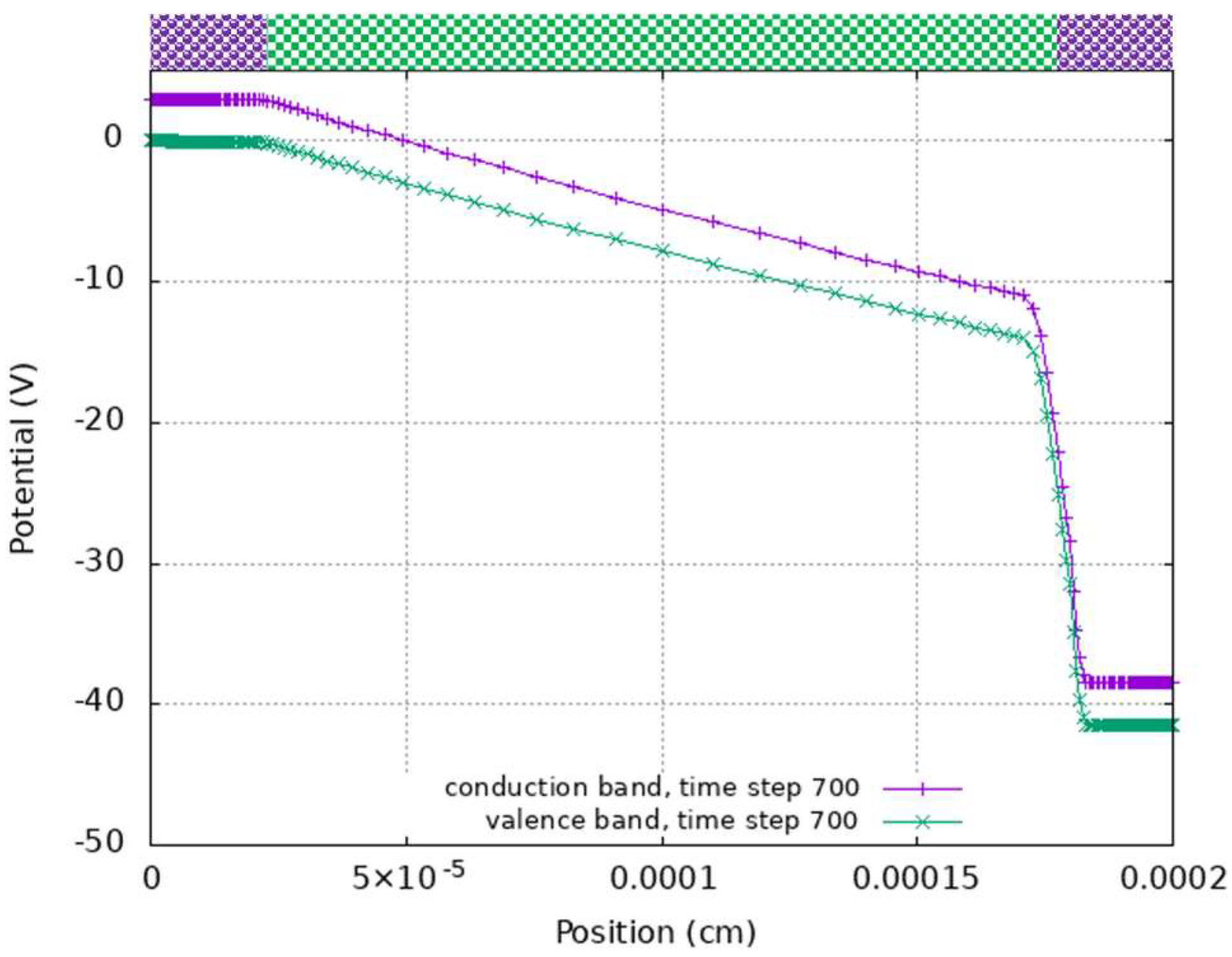
- Computational Approach
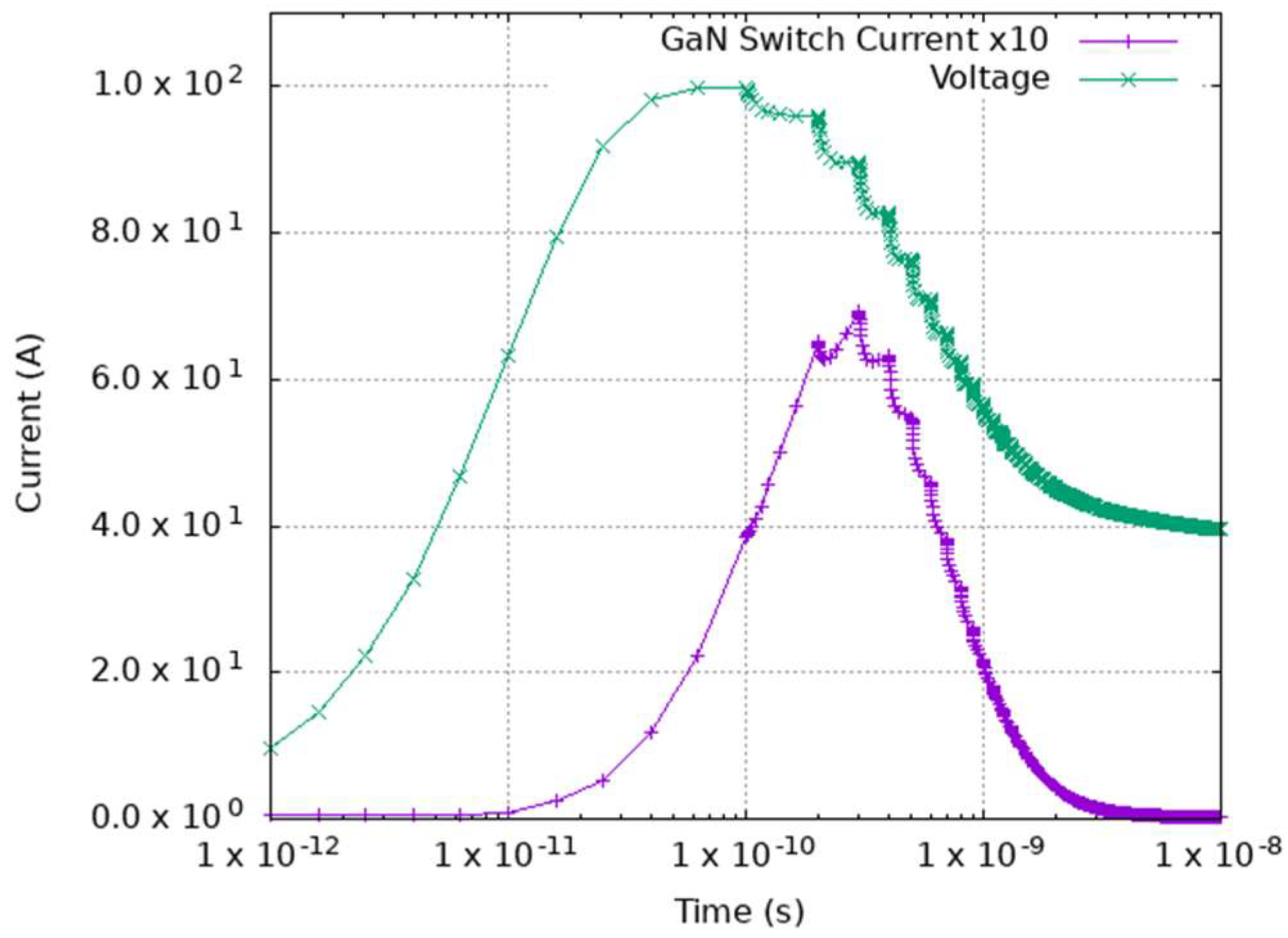
- c
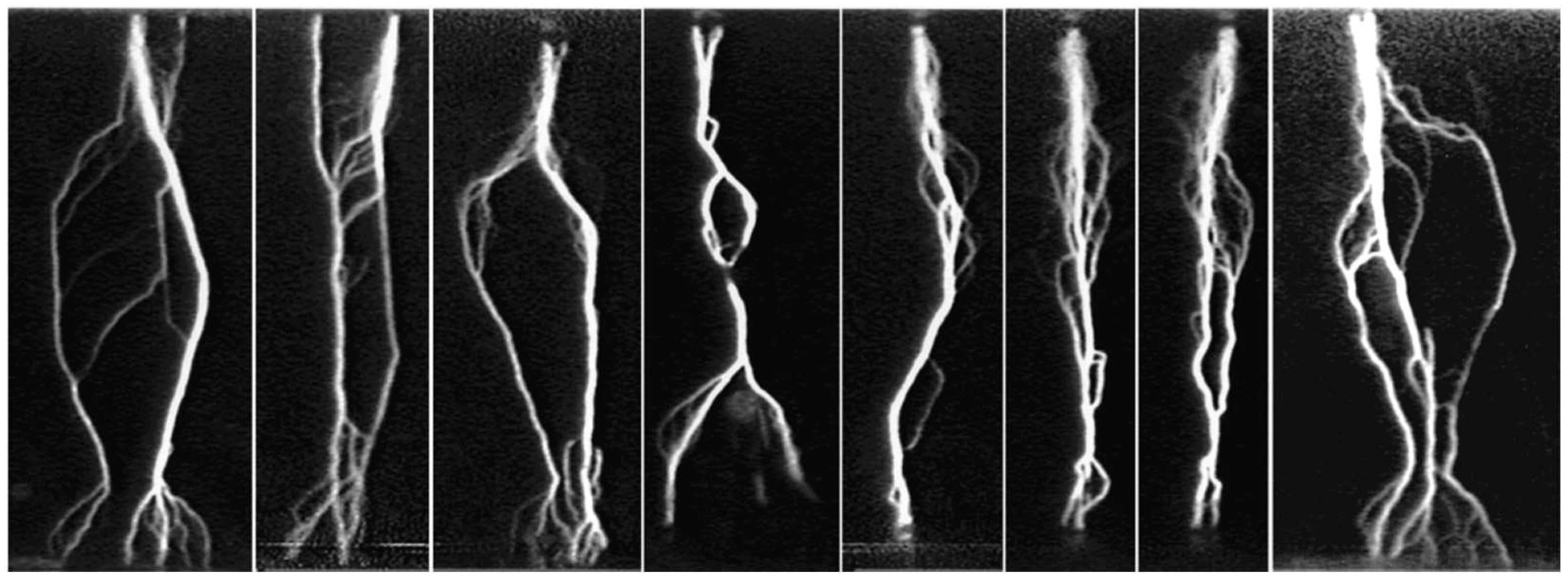
- The GaAs mechanism
- d
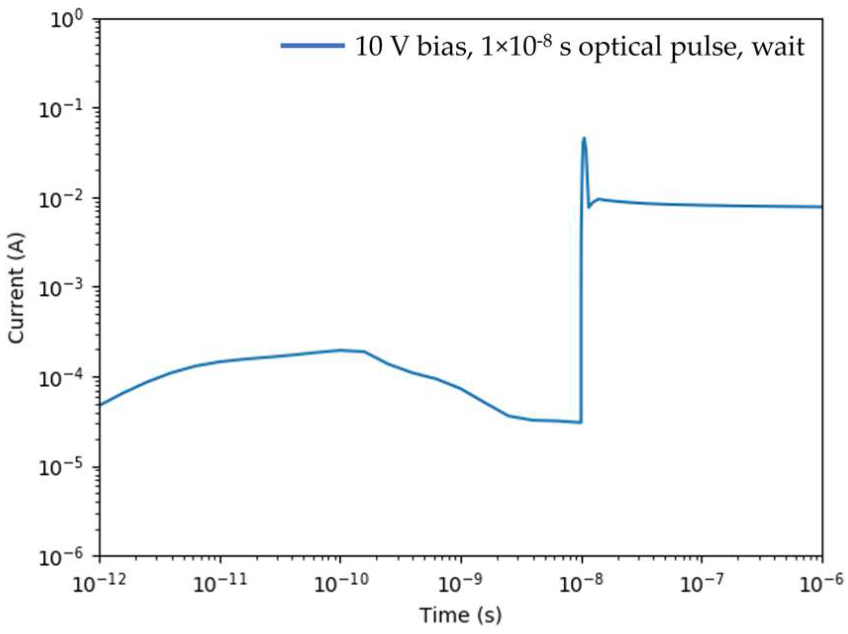
- The GaN mechanism
- e
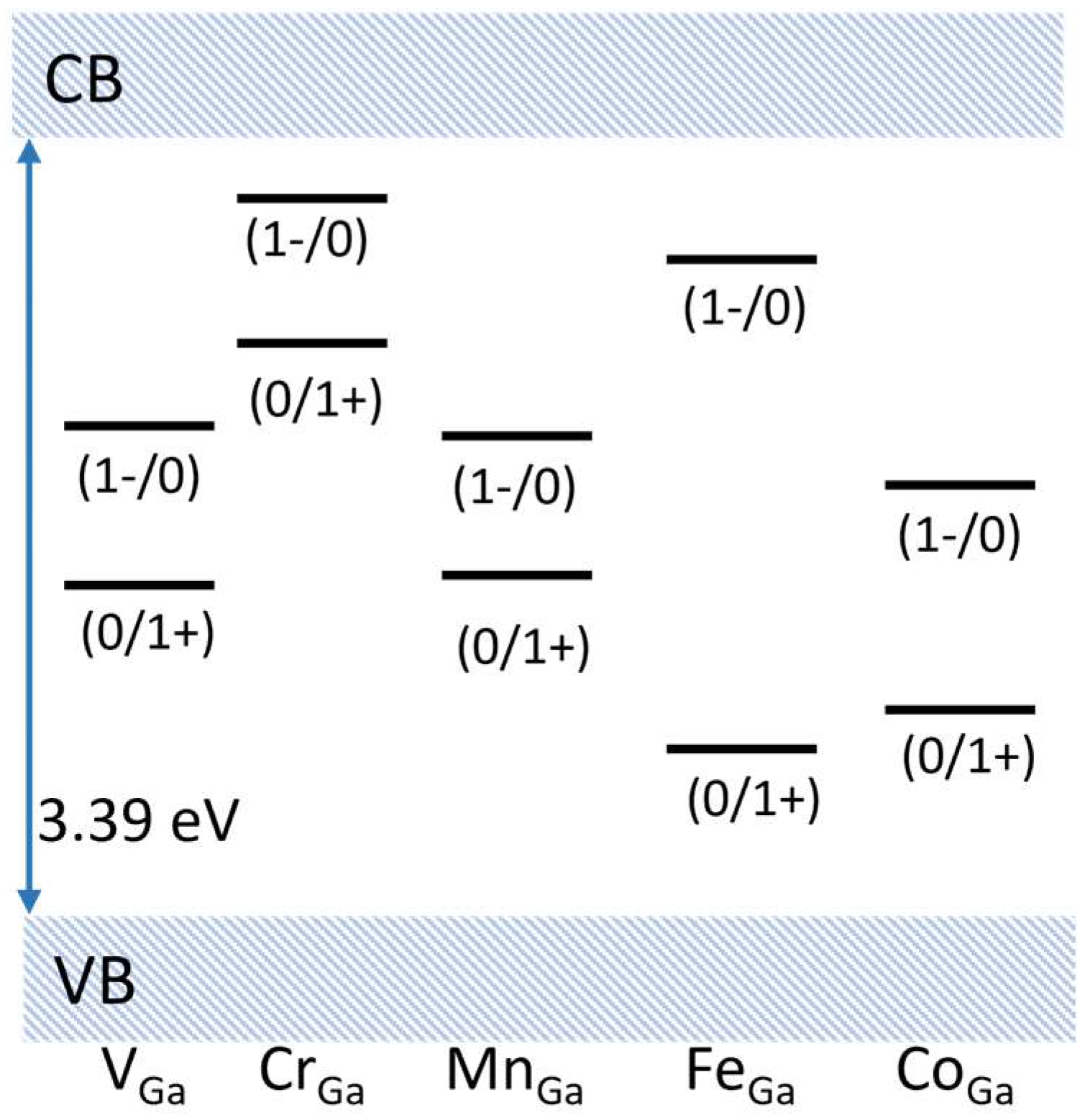
- Discussion: GaN PCSS
- f
- Comparison of lock-on mechanism: GaN and GaAs
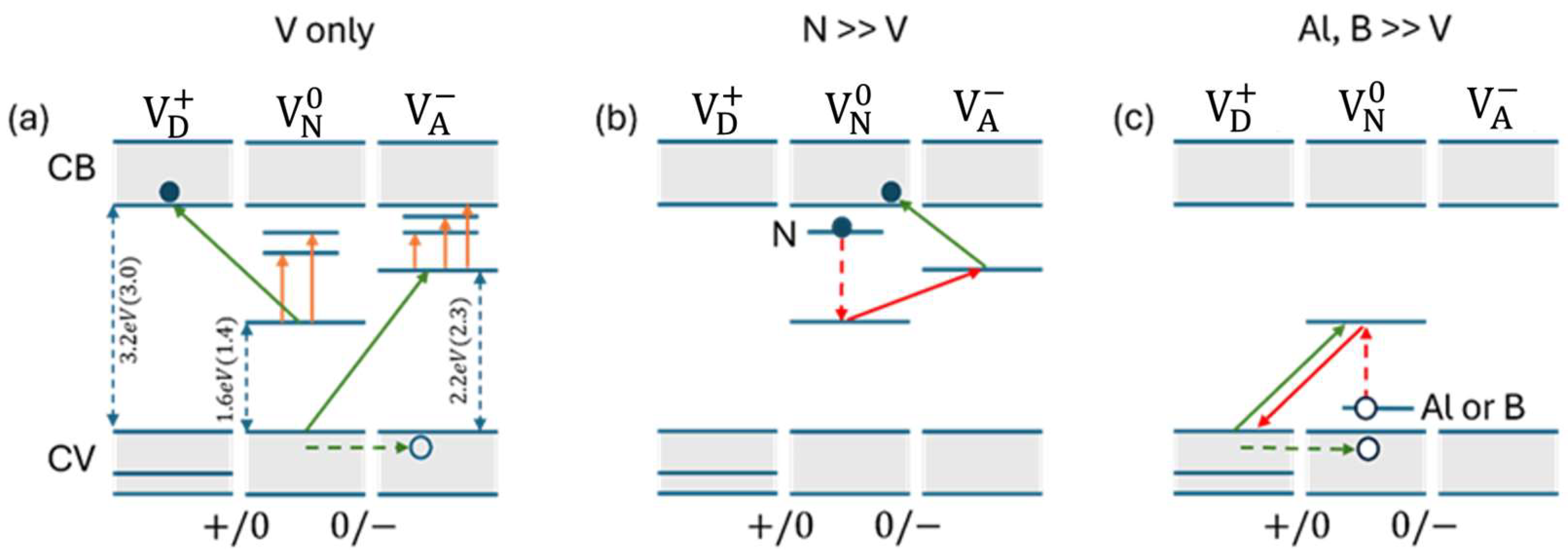
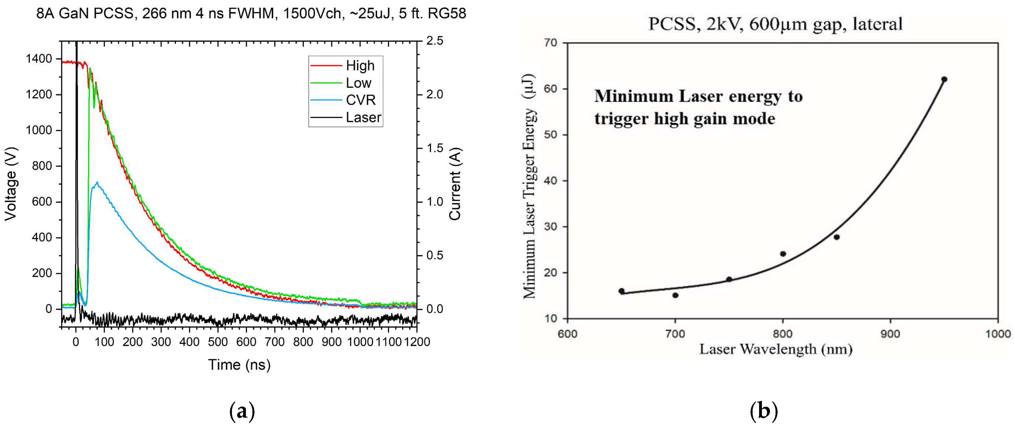
3. SiC PCSS Devices
- Doping considerations
- b
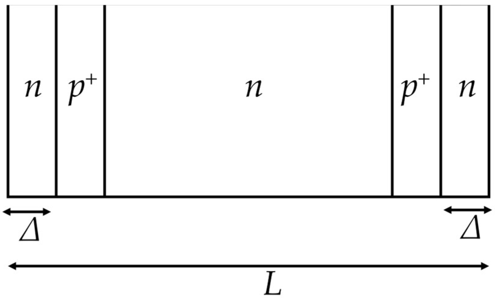
- Switch geometries

| Ref. | Material | Structure | Wavelength | ||||||
|---|---|---|---|---|---|---|---|---|---|
| [40] | 6H-SiC:V | Vertical | 532 nm | 530 kW | >150 kV/cm | 20 kV | 50 A | 244 Ω | |
| [37] | 4H-SiC:V | Vertical | 532 nm | 18.2 MW/cm2 | 260 kV/cm | 12 kV | 840 A | 7.5 Ω | |
| [41] | 6H-SiC:V | Vertical | 532 nm | 31.2 mJ, 17 ns | 225 kV/cm | 20 kV | 500 A | 5.6 Ω | Ω |
| [4] | 4H-SiC:V | Lateral | 355 nm | 1 mJ, 7 ns | 370 kV/cm | 26 kV | 450 A | 2 Ω | |
| [36] | 6H-SiC:V | Vertical | 532 nm | 4 MW | 17 kV | 1500 A | <1 Ω | Ω | |
| [39] | 4H-SiC:V | Vertical | 532 nm | 100 kW | 200 kV/cm | 20 kV | 100 A | Ω | |
| [34] | 4H:SiC:V | Lateral | 355 nm | 0.5 mJ, 7 ns | 231 kV/cm | 12.4 kV | 182 A | 12 Ω | Ω |
| [34] | 4H:SiC:V | Radial | 355 nm | 0.5 mJ, 7 ns | 178 kV/cm | 32.2 kV | 938 A | 8 Ω | Ω |
| [24] | 6H:SiC:V | Vertical | 532 nm | 13 mJ | 27.4 MV/m | 11 kV | 150 A | 2 Ω | Ω |
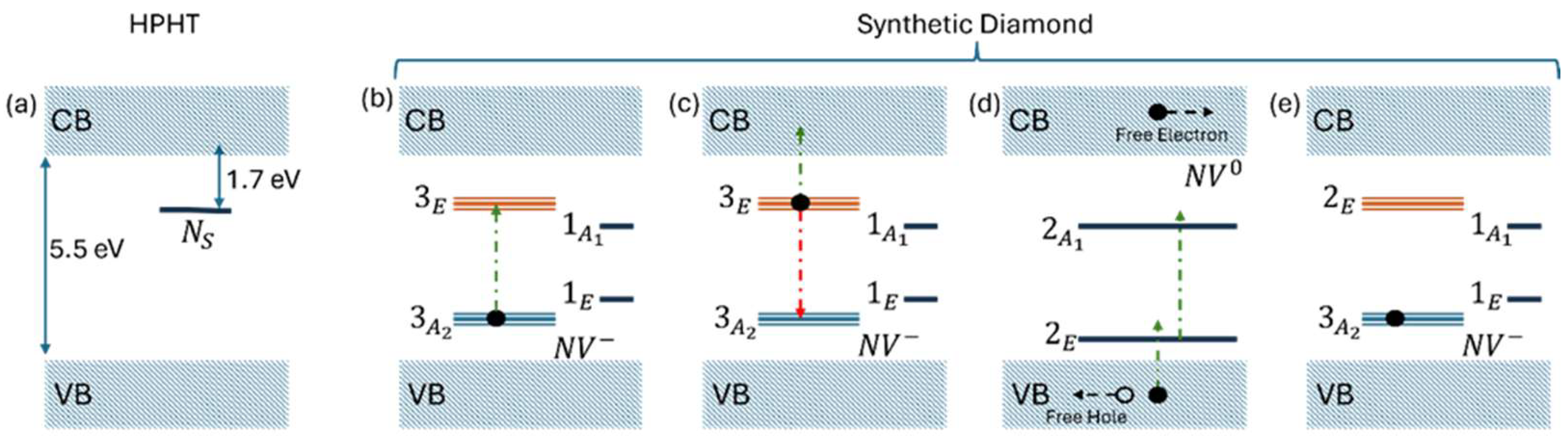
4. Diamond PCSS Devices
5. β-Ga2O3 PCSS Devices
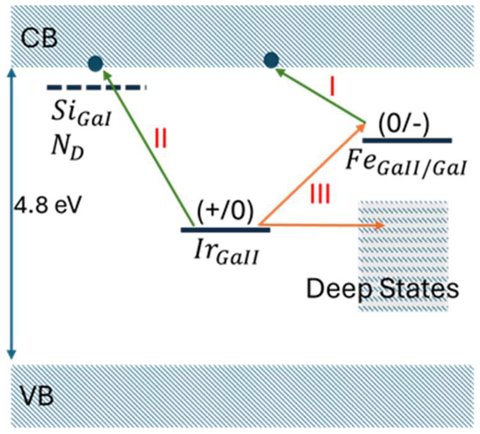
6. GaAs PCSS Devices
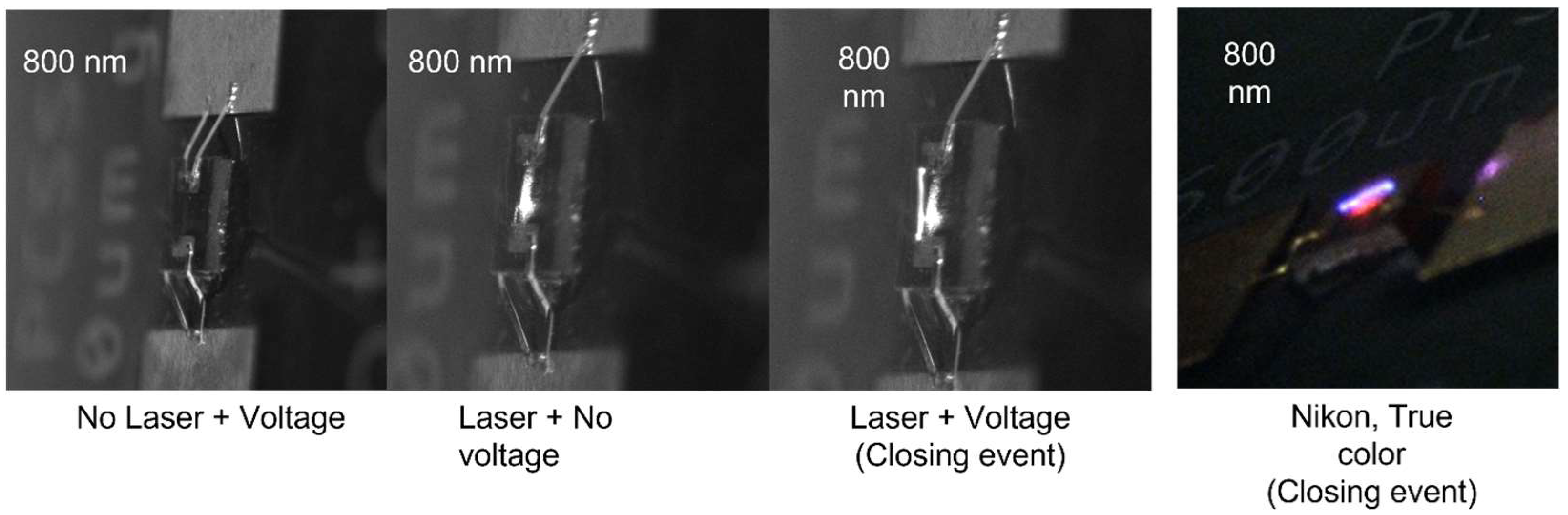
7. (Al)GaN PCSS Devices
- PCSS fabrication
- b
- PCSS performance
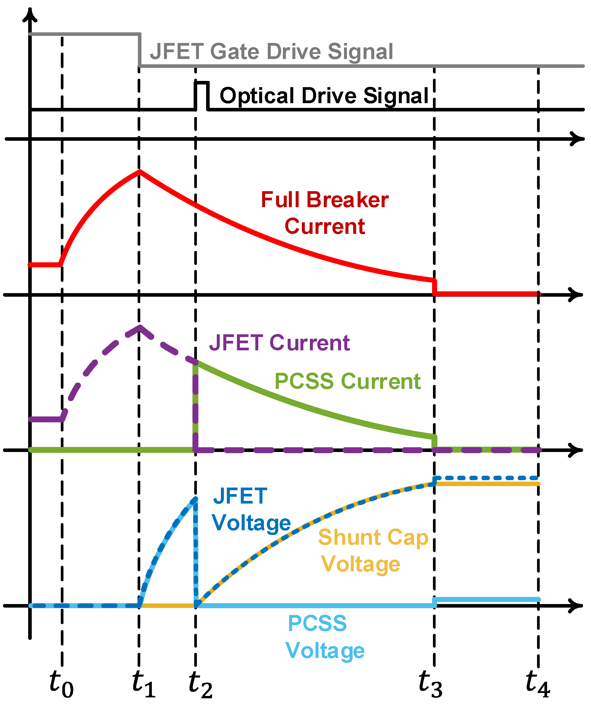
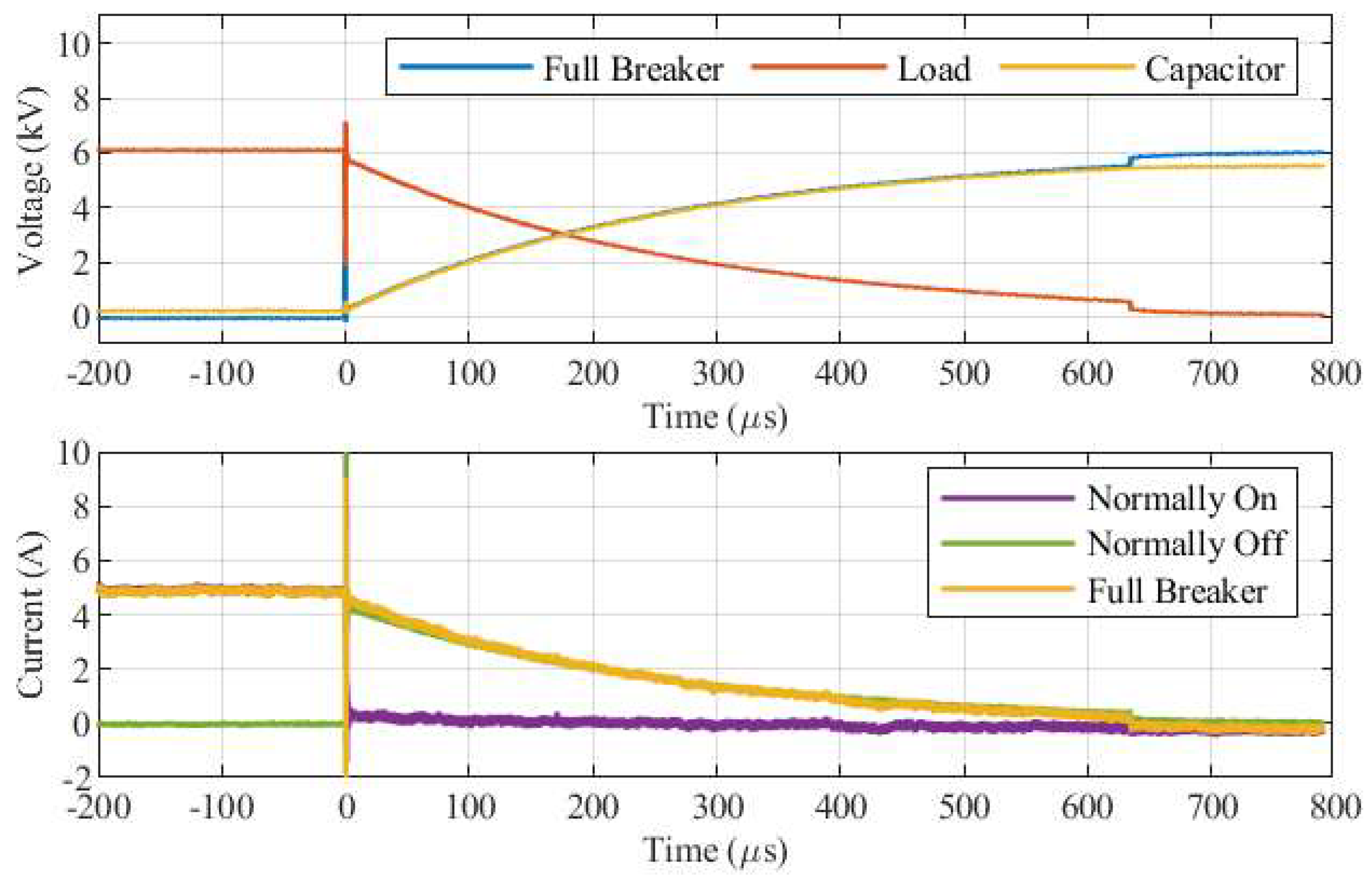
8. Application Case Study: A Medium-Voltage PCSS Breaker
8.1. SSCB Topology
8.2. Cascaded SiC JFET Switch Topology
8.3. Testing of the Integrated SSCB
9. Conclusions and Outlook
Funding
Data Availability Statement
Acknowledgments
Conflicts of Interest
References
- Majda-Zdancewicz, E.; Suproniuk, M.; Pawłowski, M.; Wierzbowski, M. Current state of photoconductive semiconductor switch engineering. Opto-Electron. Rev. 2018, 26, 92–102. [Google Scholar] [CrossRef]
- Yang, Y.; Hu, L.; Yang, X.; Zhu, Z.; Huang, J.; Yang, M.; Li, X.; Ni, L.; Zhou, Y.; Geng, L. Improved Lifetime for Kilovolts Class Avalanche GaAs PCSS by Surface Passivation of Composite Dielectric Films. IEEE Trans. Dielectr. Electr. Insul. 2024, 1–6. [Google Scholar] [CrossRef]
- Zutavern, F.J.; Loubriel, G.M.; Helgeson, W.D.; O’Malley, M.W.; Gallegos, R.R.; Hjalmarson, H.P.; Baca, A.G.; Plut, T.A. High-gain GaAs Photoconductive Semiconductor Switches (PCSS): Device Lifetime, High-Current Testing, Optical Pulse Generators; Donaldson, W.R., Ed.; SPIE: Boston, MA, USA, 1995; pp. 146–154. [Google Scholar]
- Mauch, D.; Sullivan, W.; Bullick, A.; Neuber, A.; Dickens, J. High Power Lateral Silicon Carbide Photoconductive Semiconductor Switches and Investigation of Degradation Mechanisms. IEEE Trans. Plasma Sci. 2015, 43, 2021–2031. [Google Scholar] [CrossRef]
- Loubriel, G.M.; Zutavern, F.J.; Baca, A.G.; Hjalmarson, H.P.; Plut, T.A.; Helgeson, W.D.; O’Malley, M.W.; Ruebush, M.H.; Brown, D.J. Photoconductive semiconductor switches. IEEE Trans. Plasma Sci. 1997, 25, 124–130. [Google Scholar] [CrossRef]
- Hirsch, E.A.; Mar, A.; Zutavern, F.J.; Pickrell, G.; Delhotal, J.; Gallegos, R.; Bigman, V.; Teague, J.D.; Lehr, J.M. High-Gain Persistent Nonlinear Conductivity in High-Voltage Gallium Nitride Photoconductive Switches. In Proceedings of the 2018 IEEE International Power Modulator and High Voltage Conference (IPMHVC), Jackson, WY, USA, 3–7 June 2018; IEEE: Piscataway, NJ, USA, 2018. [Google Scholar]
- Chowdhury, A.R.; Dickens, J.C.; Neuber, A.A.; Ness, R.; Joshi, R.P. Lock-on physics in semi-insulating GaAs—Combination of trap-to-band impact ionization, moving electric fields and photon recycling. J. Appl. Phys. 2018, 123, 085703. [Google Scholar] [CrossRef]
- Chowdhury, A.R.; Nikishin, S.; Dickens, J.; Neuber, A.; Joshi, R.P.; Ness, R. Numerical studies into the parameter space conducive to “lock-on” in a GaN photoconductive switch for high power applications. IEEE Trans. Dielectr. Electr. Insul. 2019, 26, 469–475. [Google Scholar] [CrossRef]
- Hjalmarson, H.; Diaz, L. Radiation Effects in Oxides and Semiconductors; Sandia National Laboratories: Albuquerque, NM, USA, 2023. [Google Scholar]
- Jung, H.K.; Taniguchi, K.; Hamaguchi, C. Impact ionization model for full band Monte Carlo simulation in GaAs. J. Appl. Phys. 1996, 79, 2473–2480. [Google Scholar] [CrossRef]
- Mar, A.; Zutavern, F.; Vawter, A.; Gallegos, R.; Bigman, V.; Hjalmarson, H. Electrical Breakdown Physics in Photoconductive Semiconductor Switches (PCSS); Sandia National Laboratories: Albuquerque, NM, USA, 2016. [Google Scholar]
- Hjalmarson, H.P.; Pease, R.L.; Witczak, S.C.; Shaneyfelt, M.R.; Schwank, J.R.; Edwards, A.H.; Hembree, C.E.; Mattsson, T.R. Mechanisms for radiation dose-rate sensitivity of bipolar transistors. IEEE Trans. Nucl. Sci. 2003, 50, 1901–1909. [Google Scholar] [CrossRef]
- Kambour, K.; Hjalmarson, H.; Zutavern, F.; Mar, A.; Myles, C.; Joshi, R. Simulation of Current Filaments in Photoconductive Semiconductor Switches. In Proceedings of the 2005 IEEE Pulsed Power Conference, Monterey, CA, USA, 13–15 June 2005; IEEE: Piscataway, NJ, USA, 2005; pp. 814–817. [Google Scholar]
- Loubriel, G.M.; Zutavern, F.J.; Mar, A.; Hjalmarson, H.P.; Baca, A.G.; O’Malley, M.W.; Helgeson, W.D.; Falk, R.A.; Brown, D.J. Longevity of optically activated, high gain GaAs photoconductive semiconductor switches. IEEE Trans. Plasma Sci. 1998, 26, 1393–1402. [Google Scholar] [CrossRef]
- Kambour, K.; Kang, S.; Myles, C.W.; Hjalmarson, H.P. Steady state properties of lock-on current filaments in GaAs [pulsed power switches]. In Proceedings of the Digest of Technical Papers. 12th IEEE International Pulsed Power Conference (Cat. No.99CH36358), Monterey, CA, USA, 27–30 June 1999; IEEE: Piscataway, NJ, USA, 1999; Volume 2, pp. 791–794. [Google Scholar]
- Brinkmann, R.P.; Schoenbach, K.H.; Stoudt, D.C.; Lakdawala, V.K.; Gerdin, G.A.; Kennedy, M.K. The lock-on effect in electron-beam-controlled gallium arsenide switches. IEEE Trans. Electron Devices 1991, 38, 701–705. [Google Scholar] [CrossRef]
- Hjalmarson, H.P.; Zutavern, F.J.; Williamson, K.M.; Lehr, J.M.; Pineda, A.C. Electrical breakdown phenomena involving material interfaces. In Proceedings of the 2013 19th IEEE Pulsed Power Conference (PPC), San Francisco, CA, USA, 16–21 June 2013; IEEE: Piscataway, NJ, USA, 2013; pp. 1–5. [Google Scholar]
- Stoklas, R.; Chvala, A.; Sichman, P.; Hasenohrl, S.; Hascik, S.; Priesol, J.; Satka, A.; Kuzmik, J. Analysis and Modeling of Vertical Current Conduction and Breakdown Mechanisms in Semi-Insulating GaN Grown on GaN: Role of Deep Levels. IEEE Trans. Electron Devices 2021, 68, 2365–2371. [Google Scholar] [CrossRef]
- Stout, P.J.; Kushner, M.J. Characteristics of an optically activated pulsed power GaAs(Si:Cu) switch obtained by two-dimensional modeling. J. Appl. Phys. 1995, 77, 3518–3522. [Google Scholar] [CrossRef]
- Schultz, P.A.; Edwards, A.H.; Van Ginhoven, R.M.; Hjalmarson, H.P.; Mounce, A.M. Theory of magnetic 3 d transition metal dopants in gallium nitride. Phys. Rev. B 2023, 107, 205202. [Google Scholar] [CrossRef]
- Maeda, T.; Narita, T.; Yamada, S.; Kachi, T.; Kimoto, T.; Horita, M.; Suda, J. Impact ionization coefficients and critical electric field in GaN. J. Appl. Phys. 2021, 129, 185702. [Google Scholar] [CrossRef]
- Doǧan, S.; Teke, A.; Huang, D.; Morkoç, H.; Roberts, C.B.; Parish, J.; Ganguly, B.; Smith, M.; Myers, R.E.; Saddow, S.E. 4H–SiC photoconductive switching devices for use in high-power applications. Appl. Phys. Lett. 2003, 82, 3107–3109. [Google Scholar] [CrossRef]
- Kelkar, K.S.; Islam, N.E.; Fessler, C.M.; Nunnally, W.C. Silicon carbide photoconductive switch for high-power, linear-mode operations through sub-band-gap triggering. J. Appl. Phys. 2005, 98, 093102. [Google Scholar] [CrossRef]
- Sullivan, J.S.; Stanley, J.R. Wide Bandgap Extrinsic Photoconductive Switches. IEEE Trans. Plasma Sci. 2008, 36, 2528–2532. [Google Scholar] [CrossRef]
- Quast, J.; Hansen, D.; Loboda, M.; Manning, I.; Moeggenborg, K.; Mueller, S.; Parfeniuk, C.; Sanchez, E.; Whiteley, C. High Quality 150 mm 4H SiC Wafers for Power Device Production. Mater. Sci. Forum 2015, 821–823, 56–59. [Google Scholar] [CrossRef]
- Evwaraye, A.O.; Smith, S.R.; Mitchel, W.C. Determination of the band offsets of the 4H–SiC/6H–SiC heterojunction using the vanadium donor (0/+) level as a reference. Appl. Phys. Lett. 1995, 67, 3319–3321. [Google Scholar] [CrossRef]
- Baur, J.; Kunzer, M.; Schneider, J. Transition Metals in SiC Polytypes, as Studied by Magnetic Resonance Techniques. Phys. Status Solidi A 1997, 162, 153–172. [Google Scholar] [CrossRef]
- Mitchel, W.C.; Perrin, R.; Goldstein, J.; Saxler, A.; Roth, M.; Smith, S.R.; Solomon, J.S.; Evwaraye, A.O. Fermi level control and deep levels in semi-insulating 4H–SiC. J. Appl. Phys. 1999, 86, 5040–5044. [Google Scholar] [CrossRef]
- Dalibor, T.; Pensl, G.; Matsunami, H.; Kimoto, T.; Choyke, W.J.; Schöner, A.; Nordell, N. Deep Defect Centers in Silicon Carbide Monitored with Deep Level Transient Spectroscopy. Phys. Status Solidi A 1997, 162, 199–225. [Google Scholar] [CrossRef]
- Mitchel, W.C.; Mitchell, W.D.; Landis, G.; Smith, H.E.; Lee, W.; Zvanut, M.E. Vanadium donor and acceptor levels in semi-insulating 4H- and 6H-SiC. J. Appl. Phys. 2007, 101, 013707. [Google Scholar] [CrossRef]
- Rakheja, S.; Huang, L.; Hau-Riege, S.; Harrison, S.E.; Voss, L.F.; Conway, A.M. Performance Modeling of Silicon Carbide Photoconductive Switches for High-Power and High-Frequency Applications. IEEE J. Electron Devices Soc. 2020, 8, 1118–1128. [Google Scholar] [CrossRef]
- Kramer, N.J.; Voss, L.F.; Conway, A.M.; Grivickas, P.V.; Bora, M.; Hall, D.L.; Caruso, A.N. Extrinsic Absorption Pathways in Vanadium-Doped SiC Measured Using a Total Internal Reflection Geometry. Phys. Status Solidi A 2020, 217, 2000315. [Google Scholar] [CrossRef]
- Hemmat, Z.; Faez, R.; Moreno, E.; Rasouli, F.; Radfar, F.; Zaimbashi, M. Transient and steady state study of a rear-illuminated 6H-SiC Photoconductive Semiconductor Switch. Optik 2016, 127, 4615–4620. [Google Scholar] [CrossRef]
- Mauch, D.; White, C.; Thomas, D.; Neuber, A.; Dickens, J. Overview of high voltage 4H-SiC photoconductive semiconductor switch efforts at Texas Tech University. In Proceedings of the 2014 IEEE International Power Modulator and High Voltage Conference (IPMHVC), Santa Fe, NM, USA, 1–5 June 2014; 2014; pp. 23–26. [Google Scholar]
- Gradinaru, G.; Sudarshan, T.S. A review on the breakdown limitation of photoconductive semiconductor power switches. In Proceedings of the 9th IEEE International Pulsed Power Conference, Albuquerque, NM, USA, 21–23 June 1993; Volume 2, p. 645. [Google Scholar]
- Sullivan, J.S. High power operation of a nitrogen doped, vanadium compensated, 6H-SiC extrinsic photoconductive switch. Appl. Phys. Lett. 2014, 104, 172106. [Google Scholar] [CrossRef]
- Cao, P.; Huang, W.; Guo, H.; Zhang, Y. Performance of a Vertical 4H-SiC Photoconductive Switch with AZO Transparent Conductive Window and Silver Mirror Reflector. IEEE Trans. Electron Devices 2018, 65, 2047–2051. [Google Scholar] [CrossRef]
- Bora, M.; Voss, L.F.; Grivickas, P.V.; Hall, D.L.; Alameda, J.B.; Kramer, N.J.; Torres, A.M.; Conway, A.M. A Total Internal Reflection Photoconductive Switch. IEEE Electron Device Lett. 2019, 40, 734–737. [Google Scholar] [CrossRef]
- Wang, B.; Wang, L.; Niu, X.; Chu, X.; Yi, M.; Yao, J.; Xun, T. Breakdown behavior of SiC photoconductive switch with transparent electrode. AIP Adv. 2022, 12, 085210. [Google Scholar] [CrossRef]
- Wang, L.; Chu, X.; Wu, Q.; Xun, T.; Yang, H.; He, J.; Zhang, J. Effects of High-Field Velocity Saturation on the Performance of V-Doped 6H Silicon-Carbide Photoconductive Switches. IEEE J. Emerg. Sel. Top. Power Electron. 2021, 9, 4879–4886. [Google Scholar] [CrossRef]
- Wu, Q.; Xun, T.; Zhao, Y.; Yang, H.; Huang, W. The Test of a High-Power, Semi-Insulating, Linear-Mode, Vertical 6H-SiC PCSS. IEEE Trans. Electron Devices 2019, 66, 1837–1842. [Google Scholar] [CrossRef]
- Han, Z.; Lee, J.; Messing, S.; Reboli, T.; Mironov, A.; Bayram, C. High Current Density Diamond Photoconductive Semiconductor Switches with a Buried, Metallic Conductive Channel. IEEE Electron Device Lett. 2024, 45, 1044–1047. [Google Scholar] [CrossRef]
- Bharadwaj, P.K.; Code, R.F.; van Driel, H.M.; Walentynowicz, E. High voltage optoelectronic switching in diamond. Appl. Phys. Lett. 1983, 43, 207–209. [Google Scholar] [CrossRef]
- Donato, N.; Rouger, N.; Pernot, J.; Longobardi, G.; Udrea, F. Diamond power devices: State of the art, modelling, figures of merit and future perspective. J. Phys. Appl. Phys. 2019, 53, 093001. [Google Scholar] [CrossRef]
- Woo, K.; Malakoutian, M.; Reeves, B.A.; Chowdhury, S. A study on sub-bandgap photoexcitation in nitrogen- and boron-doped diamond with interdigitated device structure. Appl. Phys. Lett. 2022, 120, 112104. [Google Scholar] [CrossRef]
- Curry, J.J.; Feng, S.T.; Lee, C.H.; Ho, P.T.; Goldhar, J. Photoconductive Switching in Diamond Under High Bias; Pinnow, D., Moulton, P., Eds.; Optica Publishing Group: Anaheim, CA, USA, 1988; Volume 7, p. TUM50. [Google Scholar]
- Isberg, J.; Hammersberg, J.; Johansson, E.; Wikström, T.; Twitchen, D.J.; Whitehead, A.J.; Coe, S.E.; Scarsbrook, G.A. High Carrier Mobility in Single-Crystal Plasma-Deposited Diamond. Science 2002, 297, 1670–1672. [Google Scholar] [CrossRef]
- Prasad, R.R.; Schein, J.; Gensler, S.W.; Krishnan, M. Optically Triggered Diamond Switches. In Proceedings of the Digest of Technical Papers. 12th IEEE International Pulsed Power Conference (Cat. No.99CH36358), Monterey, CA, USA, 27–30 June 1999; IEEE: Piscataway, NJ, USA, 1999; Volume 1, pp. 142–145. [Google Scholar]
- Yoneda, H.; Tokuyama, K.; Ueda, K.; Yamamoto, H.; Baba, K. High-power terahertz radiation emitter with a diamond photoconductive switch array. Appl. Opt. 2001, 40, 6733–6736. [Google Scholar] [CrossRef] [PubMed]
- Collins, A.T.; Connor, A.; Ly, C.-H.; Shareef, A.; Spear, P.M. High-temperature annealing of optical centers in type-I diamond. J. Appl. Phys. 2005, 97, 083517. [Google Scholar] [CrossRef]
- Grivickas, P.; Ščajev, P.; Kazuchits, N.; Mazanik, A.; Korolik, O.; Voss, L.F.; Conway, A.M.; Hall, D.L.; Bora, M.; Subačius, L.; et al. Carrier recombination parameters in diamond after surface boron implantation and annealing. J. Appl. Phys. 2020, 127, 245707. [Google Scholar] [CrossRef]
- Hall, D.L.; Voss, L.F.; Grivickas, P.; Bora, M.; Conway, A.M.; Ščajev, P.; Grivickas, V. Photoconductive Switch with High Sub-Bandgap Responsivity in Nitrogen-Doped Diamond. IEEE Electron Device Lett. 2020, 41, 1070–1073. [Google Scholar] [CrossRef]
- Murooka, T.; Shiigai, M.; Hironaka, Y.; Tsuji, T.; Yang, B.; Hoang, T.M.; Suda, K.; Mizuno, K.; Kato, H.; Makino, T.; et al. Photoelectrical detection of nitrogen-vacancy centers by utilizing diamond lateral p–i–n diodes. Appl. Phys. Lett. 2021, 118, 253502. [Google Scholar] [CrossRef]
- Bourgeois, E.; Jarmola, A.; Siyushev, P.; Gulka, M.; Hruby, J.; Jelezko, F.; Budker, D.; Nesladek, M. Photoelectric detection of electron spin resonance of nitrogen-vacancy centres in diamond. Nat. Commun. 2015, 6, 8577. [Google Scholar] [CrossRef]
- Heinselman, K.N.; Haven, D.; Zakutayev, A.; Reese, S.B. Projected Cost of Gallium Oxide Wafers from Edge-Defined Film-Fed Crystal Growth. Cryst. Growth Des. 2022, 22, 4854–4863. [Google Scholar] [CrossRef]
- Higashiwaki, M.; Kuramata, A.; Murakami, H.; Kumagai, Y. State-of-the-art technologies of gallium oxide power devices. J. Phys. Appl. Phys. 2017, 50, 333002. [Google Scholar] [CrossRef]
- Sasaki, K.; Kuramata, A.; Masui, T.; Víllora, E.G.; Shimamura, K.; Yamakoshi, S. Device-Quality β-Ga2O3 Epitaxial Films Fabricated by Ozone Molecular Beam Epitaxy. Appl. Phys. Express 2012, 5, 035502. [Google Scholar] [CrossRef]
- Mcglone, J.F.; Xia, Z.; Zhang, Y.; Joishi, C.; Lodha, S.; Rajan, S.; Ringel, S.A.; Arehart, A.R. Trapping Effects in Si δ-Doped β-Ga2O3 MESFETs on an Fe-Doped β-Ga2O3 Substrate. IEEE Electron Device Lett. 2018, 39, 1042–1045. [Google Scholar] [CrossRef]
- Polyakov, A.Y.; Nikolaev, V.I.; Yakimov, E.B.; Ren, F.; Pearton, S.J.; Kim, J. Deep level defect states in β-, α-, and ɛ-Ga2O3 crystals and films: Impact on device performance. J. Vac. Sci. Technol. A 2022, 40, 020804. [Google Scholar] [CrossRef]
- Bhandari, S.; Zvanut, M.E. Charge trapping at Fe due to midgap levels in Ga2O3. J. Appl. Phys. 2021, 129, 085703. [Google Scholar] [CrossRef]
- Dowling, K.M.; Chatterjee, B.; Ghandiparsi, S.; Shao, Q.; Varley, J.; Schneider, J.D.; Chapin, C.; Gottlieb, M.S.; Leos, L.; Sword, M.; et al. Evaluation of Fe-βGa2O3 for Photoconductive Semiconductor Switching. IEEE Trans. Electron Devices 2024, 71, 1535–1540. [Google Scholar] [CrossRef]
- Bhandari, S.; Zvanut, M.E.; Varley, J.B. Optical absorption of Fe in doped Ga2O3. J. Appl. Phys. 2019, 126, 165703. [Google Scholar] [CrossRef]
- Wang, Z.; Chen, X.; Ren, F.-F.; Gu, S.; Ye, J. Deep-level defects in gallium oxide. J. Phys. Appl. Phys. 2020, 54, 043002. [Google Scholar] [CrossRef]
- Zimmermann, C.; Kalmann Frodason, Y.; Rønning, V.; Varley, J.B.; Vines, L. Combining steady-state photo-capacitance spectra with first-principles calculations: The case of Fe and Ti in β-Ga2O3. New J. Phys. 2020, 22, 063033. [Google Scholar] [CrossRef]
- Singh, A.; Koksal, O.; Tanen, N.; McCandless, J.; Jena, D.; Xing, H.; Peelaers, H.; Rana, F. Ultrafast dynamics of gallium vacancy charge states in beta Ga2O3. Phys. Rev. Res. 2021, 3, 023154. [Google Scholar] [CrossRef]
- Nunnally, W.C.; Hammond, R.B. Photoconductive Power Switches. In Proceedings of the 27th Annual Technical Symposium, San Diego, CA, USA, 23–25 August 1983; Mourou, G.A., Ed.; SPIE: Bellingham, WA, USA; pp. 116–122. [Google Scholar]
- Kawase, T.; Hagi, Y.; Tatsumi, M.; Fujita, K.; Nakai, R. Low-dislocation-density and low-residual-strain semi-insulating GaAs grown by vertical boat method. In Proceedings of the Semiconducting and Semi-Insulating Materials Conference, Toulouse, France, 29 April–3 May 1996; IEEE: Piscataway, NJ, USA, 1996; pp. 275–278. [Google Scholar]
- Bünger, T.; Behr, D.; Eichler, S.; Flade, T.; Fliegel, W.; Jurisch, M.; Kleinwechter, A.; Kretzer, U.; Steinegger, T.; Weinert, B. Development of a vertical gradient freeze process for low EPD GaAs substrates. Mater. Sci. Eng. B 2001, 80, 5–9. [Google Scholar] [CrossRef]
- Wang, X.; Mazumder, S.K. A photoconductive semiconductor switch vertically embedded with MISFETs for high-power high-repetition-rate application. In Proceedings of the 2015 IEEE 6th International Symposium on Power Electronics for Distributed Generation Systems (PEDG), Aachen, Germany, 22–25 June 2015; IEEE: Piscataway, NJ, USA, 2015; pp. 1–5. [Google Scholar]
- Gaudet, J.A.; Prather, W.D.; Burger, J.; Skipper, M.C.; Abdalla, M.D.; Mar, A.; O’Malley, M.W.; Zutavern, F.J.; Loubriel, G.M. Progress in gallium arsenide photoconductive switch research for high power applications. In Proceedings of the Conference Record of the Twenty-Fifth International Power Modulator Symposium, 2002 and 2002 High-Voltage Workshop, Hollywood, CA, USA, 30 June–3 July 2002; IEEE: Piscataway, NJ, USA, 2002; pp. 699–702. [Google Scholar]
- Shi, W.; Tian, L.; Liu, Z.; Zhang, L.; Zhang, Z.; Zhou, L.; Liu, H.; Xie, W. 30 kV and 3 kA semi-insulating GaAs photoconductive semiconductor switch. Appl. Phys. Lett. 2008, 92, 043511. [Google Scholar] [CrossRef]
- Zutavern, F.J.; Glover, S.F.; Mar, A.; Cich, M.J.; Loubriel, G.M.; Swalby, M.E.; Collins, R.T.; Greives, K.H.; Keator, N.D. High current, multi-filament photoconductive semiconductor switching. In Proceedings of the 2011 IEEE Pulsed Power Conference, Chicago, IL, USA, 19–23 June 2011; IEEE: Piscataway, NJ, USA, 2011; pp. 1112–1119. [Google Scholar]
- Mar, A.; Zutavern, F.; Hjalmarson, H.; Vawter, G.A.; Gallegos, R. Advanced High-Longevity GaAs Photoconductive Semiconductor Switches; Directed Energy Professional Society: Anaheim, CA, USA, 2015. [Google Scholar]
- Loubriel, G.M.; Omalley, M.M.; Zutavern, F.J. Toward pulsed power uses for photoconductive semiconductor switches: Closing switches. In Proceedings of the 6th Institute of Electrical and Electronic Engineers Pulsed Power Conference, Arlington, VA, USA, 29 June–1 July 1987; IEEE: Piscataway, NJ, USA, 1987. [Google Scholar]
- Zutavern, F.J.; Loubriel, G.M.; McLaughlin, D.L.; Helgeson, W.D.; O’Malley, M.W. Electrical and optical properties of high-gain GaAs switches. In Proceedings of the OE/LASE ’92, Los Angeles, CA, USA, 19–24 January 1992; Loubriel, G.M., Ed.; SPIE: Bellingham, WA, USA, 1992; p. 152. [Google Scholar]
- Schoenberg, J.S.H.; Burger, J.W.; Tyo, J.S.; Abdalla, M.D.; Skipper, M.C.; Buchwald, W.R. Ultra-wideband source using gallium arsenide photoconductive semiconductor switches. IEEE Trans. Plasma Sci. 1997, 25, 327–334. [Google Scholar] [CrossRef]
- Lehr, J.M.; Ahern, S.M.; Abdalla, M.D.; Skipper, M.C.; Romero, S.P.; Gaudet, J.A.; Burger, J.W.; Hull, J.P.; Gruner, F.R.; Cockerham, B.D.; et al. Marx generator triggering with photoconductive switches. In Proceedings of the AeroSense 2000, Orlando, FL, USA, 24–28 April 2000; Brandt, H.E., Ed.; SPIE: Bellingham, WA, USA, 2000; pp. 175–184. [Google Scholar]
- Amano, H.; Baines, Y.; Beam, E.; Borga, M.; Bouchet, T.; Chalker, P.R.; Charles, M.; Chen, K.J.; Chowdhury, N.; Chu, R.; et al. The 2018 GaN power electronics roadmap. J. Phys. Appl. Phys. 2018, 51, 163001. [Google Scholar] [CrossRef]
- Koehler, A.D.; Anderson, T.J.; Khachatrian, A.; Nath, A.; Tadjer, M.J.; Buchner, S.P.; Hobart, K.D.; Kub, F.J. High Voltage GaN Lateral Photoconductive Semiconductor Switches. ECS J. Solid State Sci. Technol. 2017, 6, S3099. [Google Scholar] [CrossRef]
- Chen, Y.; Lu, H.; Chen, D.; Ren, F.; Zhang, R.; Zheng, Y. High-voltage photoconductive semiconductor switches fabricated on semi-insulating HVPE GaN:Fe template. Phys. Status Solidi C 2016, 13, 374–377. [Google Scholar] [CrossRef]
- Meyers, V.; Mauch, D.; Kuryatkov, V.; Nikishin, S.; Dickens, J.; Neuber, A.; Ness, R. Toward the development of an efficient bulk semi-insulating GaN photoconductive switch. In Proceedings of the 2017 IEEE 21st International Conference on Pulsed Power (PPC), Brighton, UK, 18–22 June 2017; IEEE: Piscataway, NJ, USA, 2017; pp. 1–4. [Google Scholar]
- Liu, G.; Zhou, G.; Qin, Z.; Zhou, Q.; Zheng, R.; Wu, H.; Sun, Z. Luminescence characterizations of freestanding bulk single crystalline aluminum nitride towards optoelectronic application. CrystEngComm 2017, 19, 5522–5527. [Google Scholar] [CrossRef]
- Bondokov, R.T.; Hogan, K.; Norbury, G.Q.; Mark, J.; Branagan, S.P.; Ishigami, N.; Grandusky, J.; Chen, J. (Jeff) (Invited) Development of 3-inch AlN Single Crystal Substrates. ECS Trans. 2022, 109, 13–19. [Google Scholar] [CrossRef]
- Meyer, J.R.; Kruer, M.R.; Bartoli, F.J. Optical heating in semiconductors: Laser damage in Ge, Si, InSb, and GaAs. J. Appl. Phys. 1980, 51, 5513–5522. [Google Scholar] [CrossRef]
- Nune, R.; Anurag, A.; Anand, S.; Chauhan, Y.S. Comparative analysis of power density in Si MOSFET and GaN HEMT based flyback converters. In Proceedings of the 2016 10th International Conference on Compatibility, Power Electronics and Power Engineering (CPE-POWERENG), Bydgoszcz, Poland, 29 June–1 July 2016; IEEE: Piscataway, NJ, USA, 2016; pp. 347–352. [Google Scholar]
- BREAKERS: Building Reliable Electronics to Achieve Kilovolt Effective Ratings Safely. Available online: https://arpa-e.energy.gov/technologies/programs/breakers (accessed on 9 December 2023).
- Lehr, J.; Gonzalez, N.; Maynard, B.; Gallegos, R.; Hjalmarson, H.; Kaplar, R.; Mar, A.; Schrock, E.; Pickrell, G. Investigating Lock on in Gallium Nitride Photoconductive Solid State Switches; Sandia National Lab. (SNL-NM): Albuquerque, NM, USA, 2021; No. SAND2021-15818C. [Google Scholar]
- Flicker, J.D.; Garcia Rodriguez, L.A.; Mueller, J.; Gill, L.; Neely, J.C.; Schrock, E.; Hjalmarson, H.P.; Bellotti, E.; Schultz, P.A.; Lehr, J.M.; et al. Light-Triggered Solid-State Circuit Breaker for DC Electrical Systems. In Direct Current Fault Protection; Kizilyalli, I.C., Shen, Z.J., Cunningham, D.W., Eds.; Springer International Publishing: Cham, Switzerland, 2023; pp. 185–222. ISBN 978-3-031-26571-6. [Google Scholar]
- Korotkov, R.Y.; Gregie, J.M.; Wessels, B.W. Optical properties of the deep Mn acceptor in GaN:Mn. Appl. Phys. Lett. 2002, 80, 1731–1733. [Google Scholar] [CrossRef]
- Yao, X. Study on DC arc faults in ring-bus DC microgrids with constant power loads. In Proceedings of the 2016 IEEE Energy Conversion Congress and Exposition (ECCE), Milwaukee, WI, USA, 18–22 September 2016; IEEE: Piscataway, NJ, USA, 2016; pp. 1–5. [Google Scholar]
- Baran, M.E.; Mahajan, N.R. DC distribution for industrial systems: Opportunities and challenges. IEEE Trans. Ind. Appl. 2003, 39, 1596–1601. [Google Scholar] [CrossRef]
- Pei, X.; Cwikowski, O.; Vilchis-Rodriguez, D.S.; Barnes, M.; Smith, A.C.; Shuttleworth, R. A review of technologies for MVDC circuit breakers. In Proceedings of the IECON 2016—42nd Annual Conference of the IEEE Industrial Electronics Society, Florence, Italy, 23–26 October 2016; IEEE: Piscataway, NJ, USA, 2016; pp. 3799–3805. [Google Scholar]
- Shukla, A.; Demetriades, G.D. A Survey on Hybrid Circuit-Breaker Topologies. IEEE Trans. Power Deliv. 2015, 30, 627–641. [Google Scholar] [CrossRef]
- 35 mΩ-1200V SiC Normally-On JFET, UJ3N120035K3S; Qorvo (formerly United SiC): Greensboro, NC, USA, 2018.
- Garcia Rodriguez, L.A.; Gill, L.; Mueller, J.A.; Neely, J.; Baker, G.; Flicker, J.; Schrock, E.; Pickrell, G.; Kaplar, R. Cascaded SiC JFET Topology for High-Voltage Solid-State Circuit Breaker Applications. IEEE Trans. Ind. Appl. 2023, 59, 2326–2339. [Google Scholar] [CrossRef]
- Zutavern, F.J.; Glover, S.F.; Reed, K.W.; Cich, M.J.; Mar, A.; Swalby, M.E.; Saiz, T.A.; Horry, M.L.; Gruner, F.R.; White, F.E. PCSS triggered pulsed power switches. In Proceedings of the 2007 16th IEEE International Pulsed Power Conference, Albuquerque, NM, USA, 17–22 June 2007; IEEE: Piscataway, NJ, USA, 2007; pp. 231–235. [Google Scholar]


| Property | Si | GaAs | 4H-SiC | GaN | AlN | β-GA2O3 | Diamond |
|---|---|---|---|---|---|---|---|
| Bandgap (eV), Direct or Indirect (d, i) | 1.11, i | 1.43, d | 3.26, i | 3.39, d | 6.1, d | 4.5, i | 5.47, d or i |
| Breakdown Electric Field (MV/cm) | 0.3 | 0.4 | 2.0 | 3.3 | 11.7 | 7 | 10 |
| Electron Mobility (cm2 V−1s−1) | 1400 | 8500 | 700 | 900 | 1100 | 200 | 4500 |
| Saturation Drift Velocity (×107 cm/s) | 1.0 | 1.0 | 2.0 | 2.5 | 1.8 | 1.7 | 2.0 |
| Relative Permittivity | 11.8 | 12.9 | 9.7 | 9.5 | 8.7 | 10 | 5.7 |
| Thermal Conductivity (W/cm K) | 1.5 | 0.5 | 4.5 | 1.3 | 2.5 | 0.2 | 2.2 |
| Maximum Operable Junction Temperature (°C) | 300 | 300 | 1600 | 500 | 1000 | 1700 | 700 |
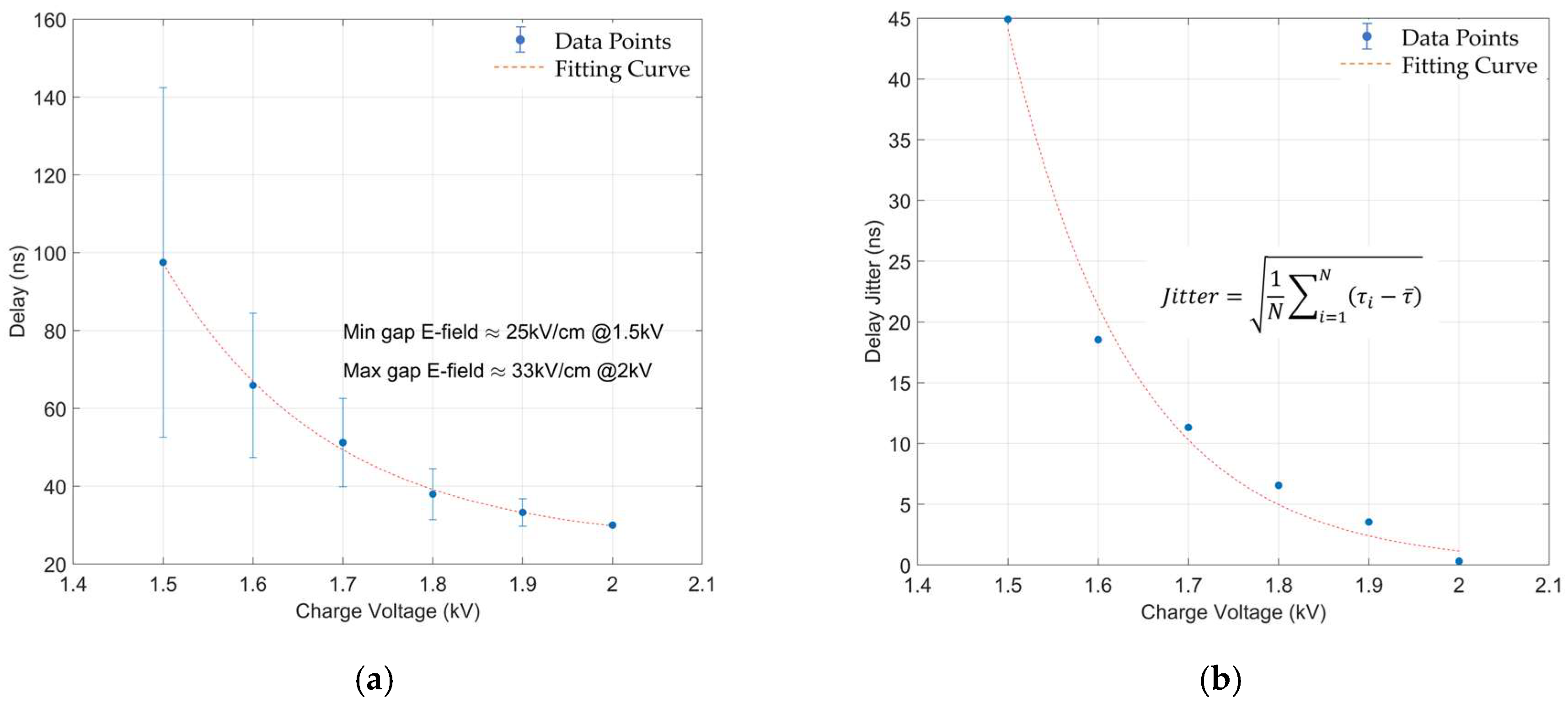
| Dopant | Min. Trigger Energy [μJ] | Mean Delay [ns] | Jitter [ns] | Reliability [%] |
|---|---|---|---|---|
| Mn | 22.5 | 27.8 | 2.1 | 100 |
| Fe | 1500 | 58 | 12.4 | 35 |
Disclaimer/Publisher’s Note: The statements, opinions and data contained in all publications are solely those of the individual author(s) and contributor(s) and not of MDPI and/or the editor(s). MDPI and/or the editor(s) disclaim responsibility for any injury to people or property resulting from any ideas, methods, instructions or products referred to in the content. |
© 2025 by the authors. Licensee MDPI, Basel, Switzerland. This article is an open access article distributed under the terms and conditions of the Creative Commons Attribution (CC BY) license (https://creativecommons.org/licenses/by/4.0/).
Share and Cite
Meyers, V.; Voss, L.; Flicker, J.D.; Rodriguez, L.G.; Hjalmarson, H.P.; Lehr, J.; Gonzalez, N.; Pickrell, G.; Ghandiparsi, S.; Kaplar, R. Photoconductive Semiconductor Switches: Materials, Physics, and Applications. Appl. Sci. 2025, 15, 645. https://doi.org/10.3390/app15020645
Meyers V, Voss L, Flicker JD, Rodriguez LG, Hjalmarson HP, Lehr J, Gonzalez N, Pickrell G, Ghandiparsi S, Kaplar R. Photoconductive Semiconductor Switches: Materials, Physics, and Applications. Applied Sciences. 2025; 15(2):645. https://doi.org/10.3390/app15020645
Chicago/Turabian StyleMeyers, Vincent, Lars Voss, Jack D. Flicker, Luciano Garcia Rodriguez, Harold P. Hjalmarson, Jane Lehr, Nicolas Gonzalez, Gregory Pickrell, Soroush Ghandiparsi, and Robert Kaplar. 2025. "Photoconductive Semiconductor Switches: Materials, Physics, and Applications" Applied Sciences 15, no. 2: 645. https://doi.org/10.3390/app15020645
APA StyleMeyers, V., Voss, L., Flicker, J. D., Rodriguez, L. G., Hjalmarson, H. P., Lehr, J., Gonzalez, N., Pickrell, G., Ghandiparsi, S., & Kaplar, R. (2025). Photoconductive Semiconductor Switches: Materials, Physics, and Applications. Applied Sciences, 15(2), 645. https://doi.org/10.3390/app15020645