
Study on Single-Event Transient Hardness of Semi-Enclosed Gate NMOS

Abstract
:1. Introduction
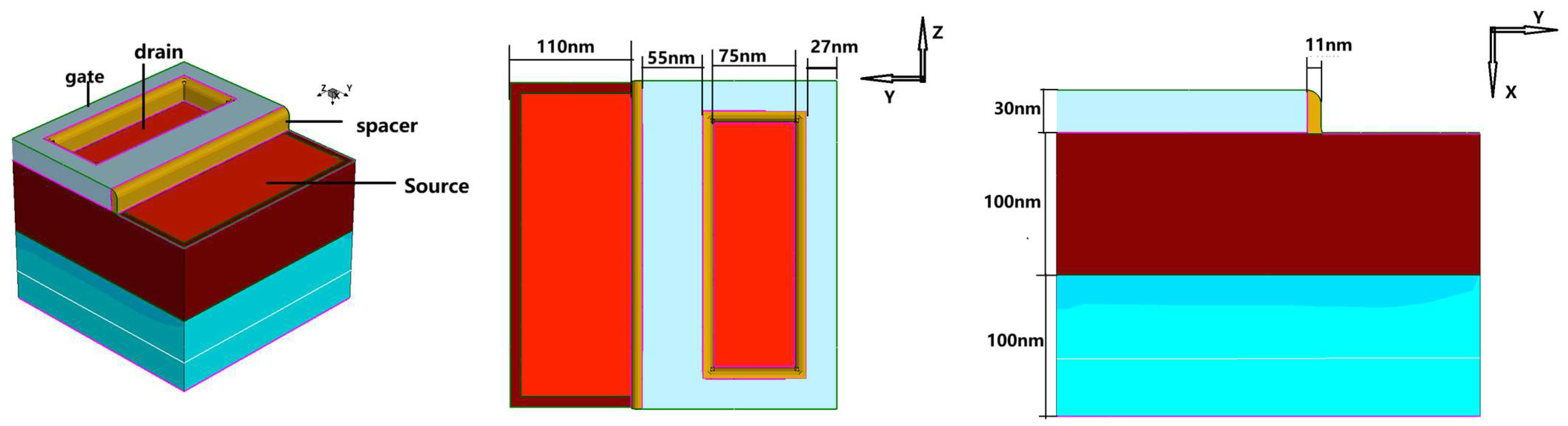
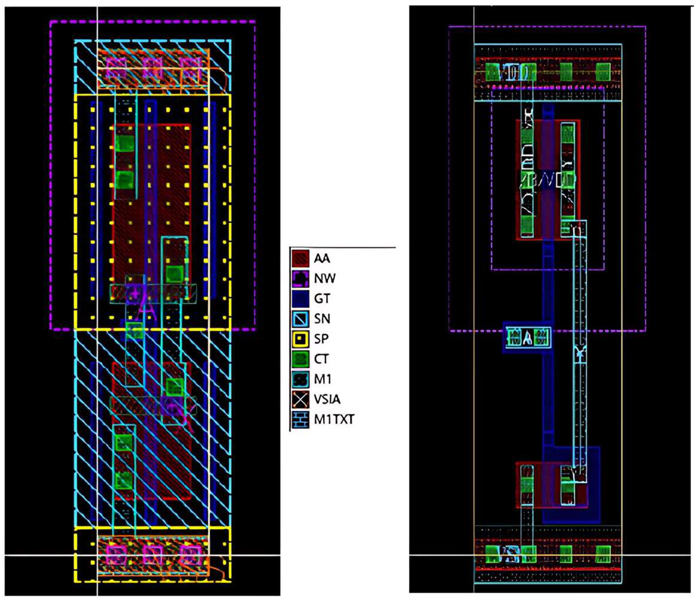
2. Simulation Setup
3. Analysis of Simulation Results
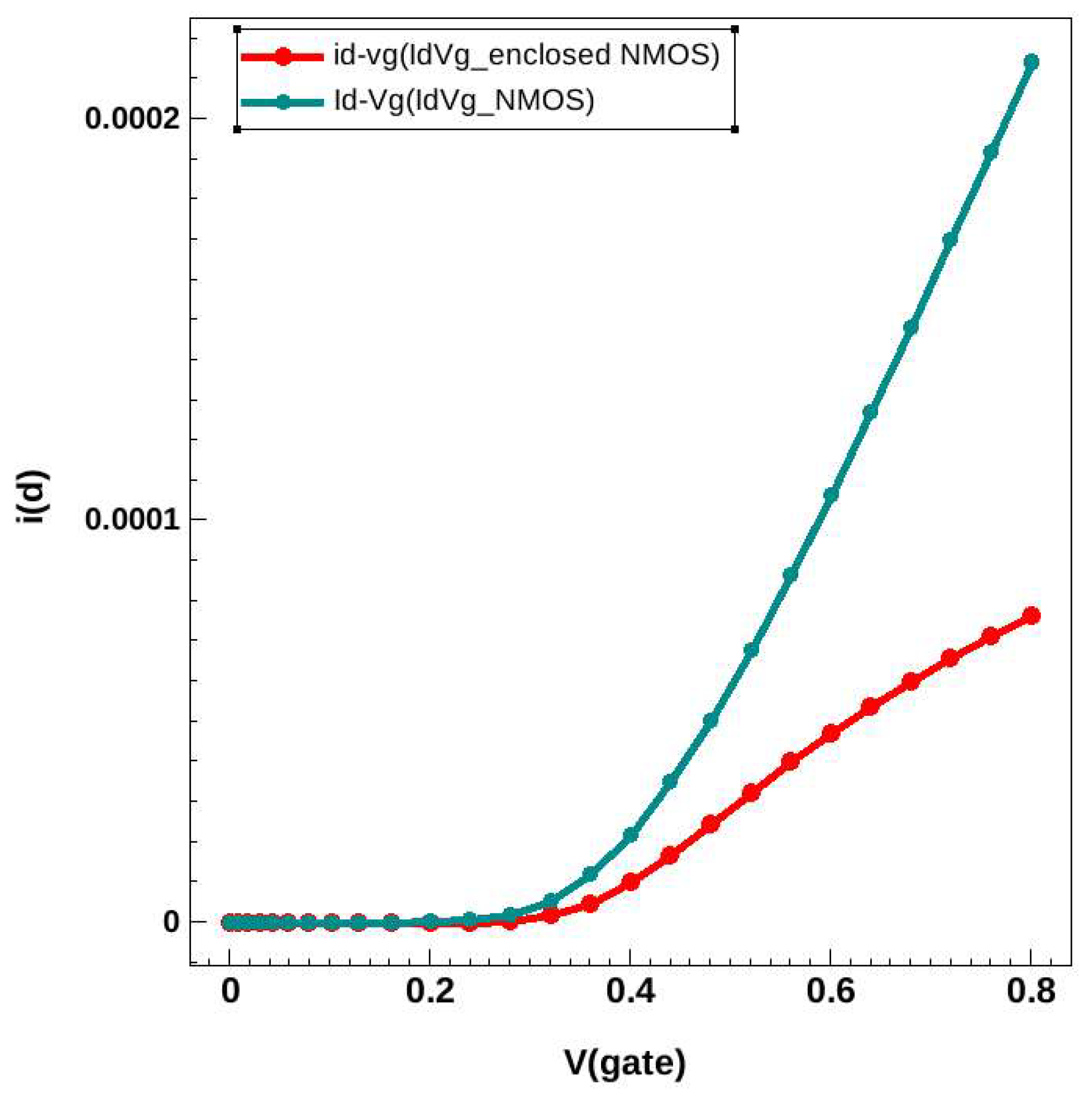
3.1. Simulation and Analysis of Single-Event Transients in Conventional NMOS vs. Semi-Enclosed NMOS
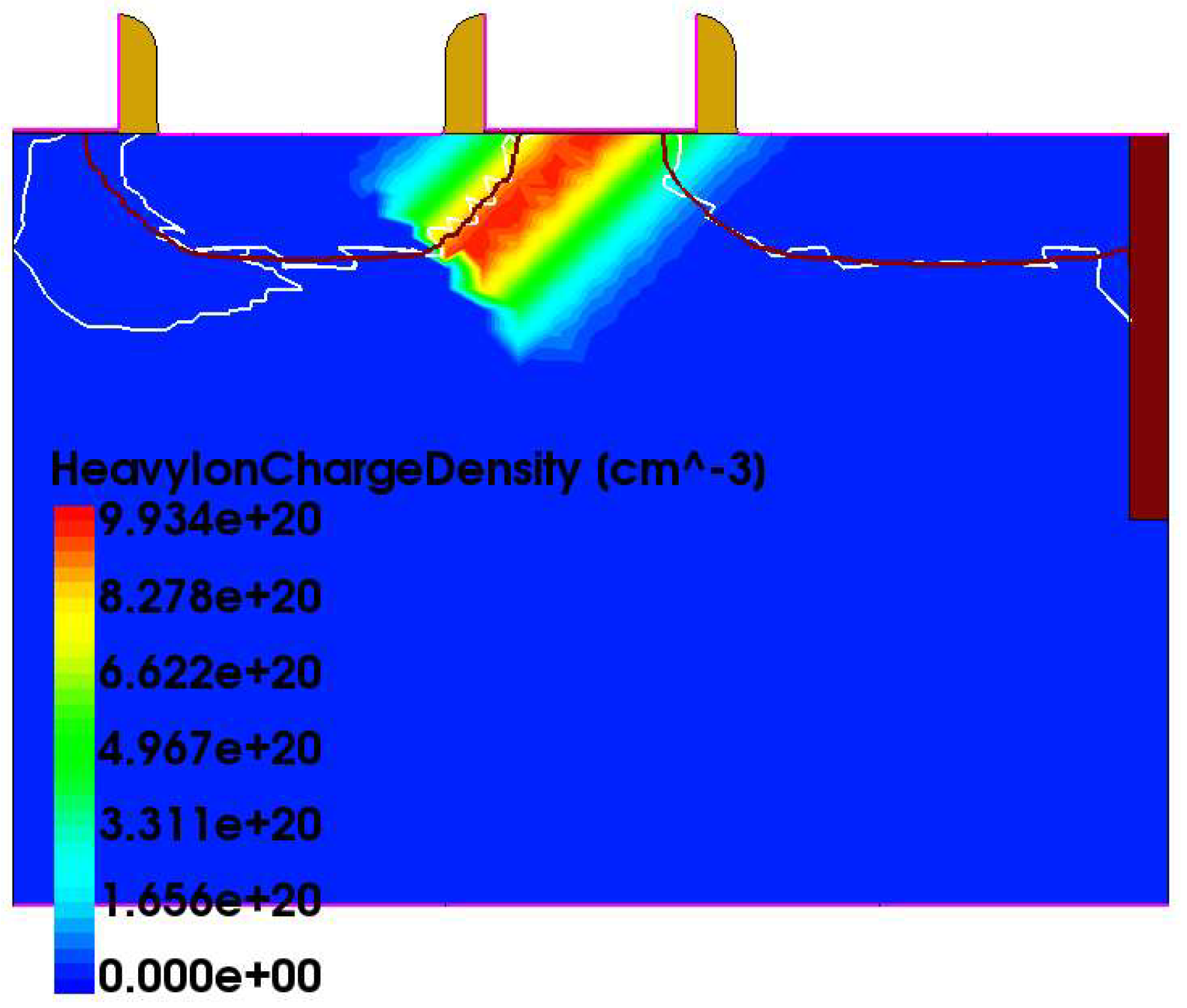
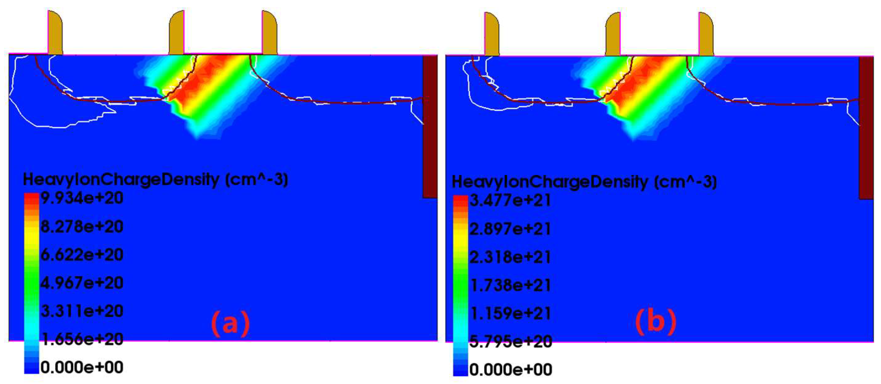
3.2. Analysis of Heavy Particle Irradiation with Different LETs and Internal Mechanisms
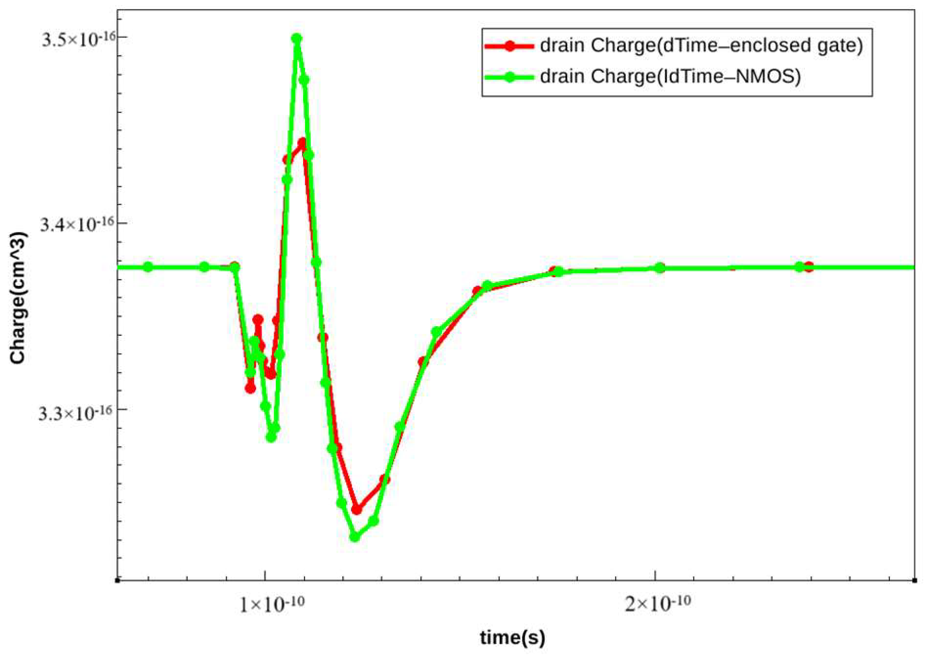
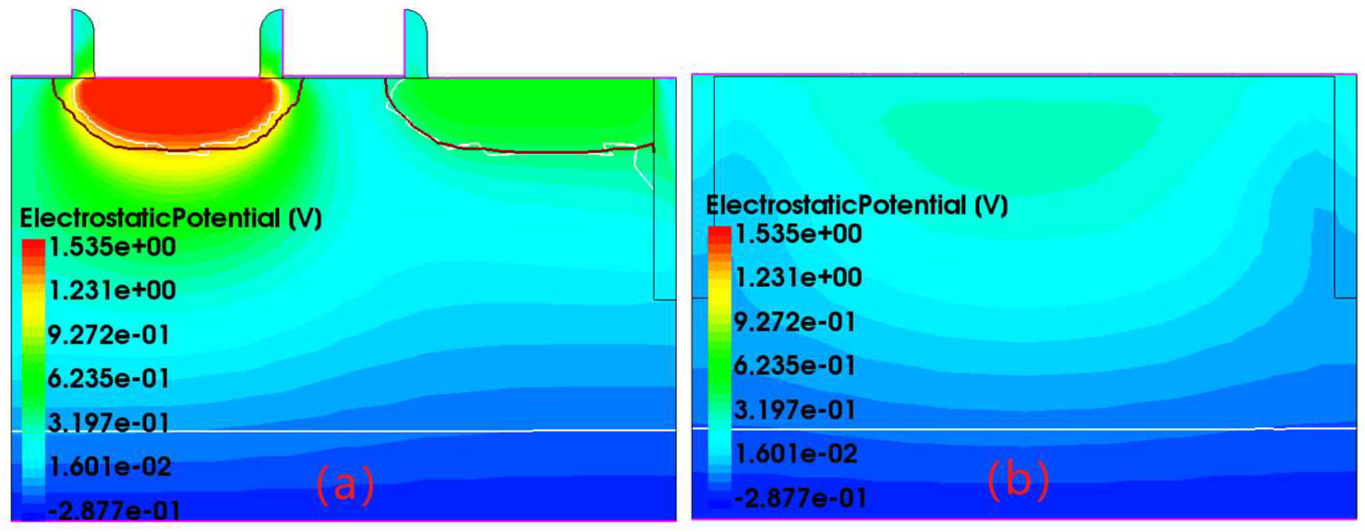
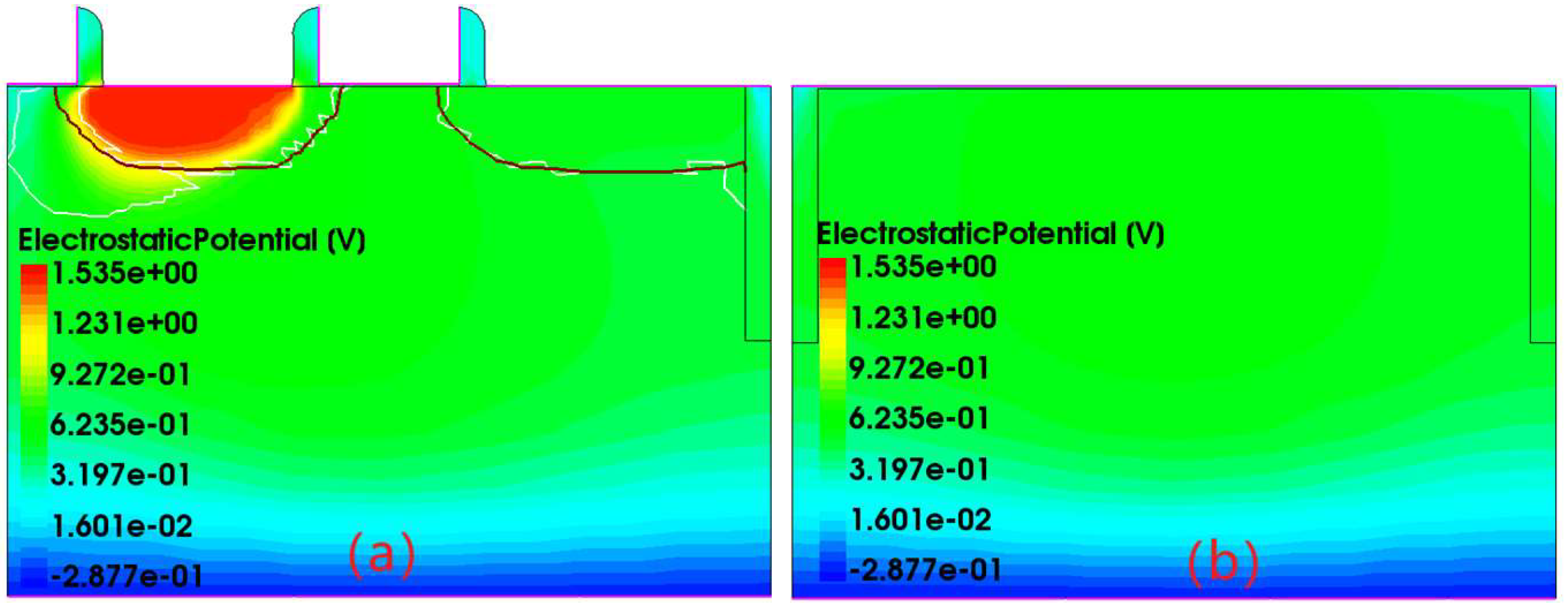
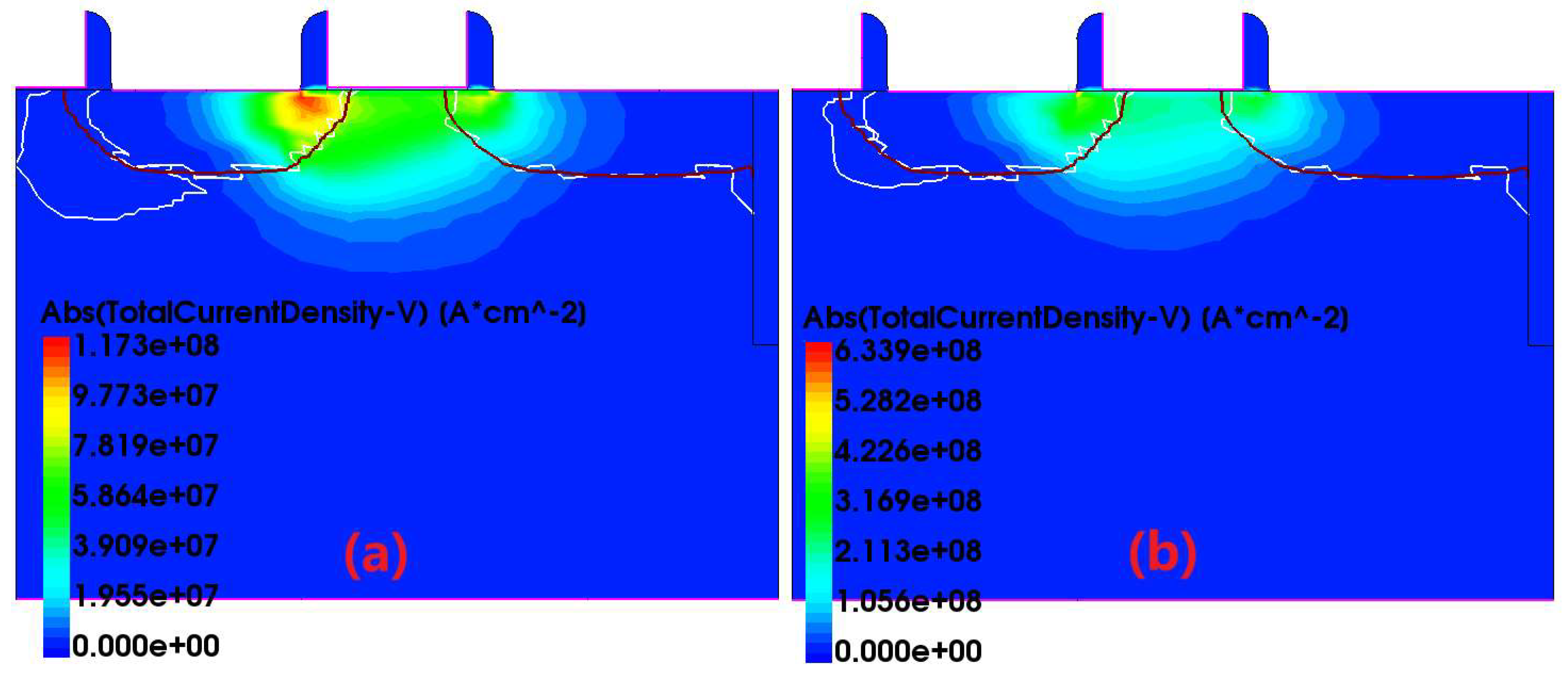
3.3. Analysis of Electric Potential Gradient Distribution at Different Times
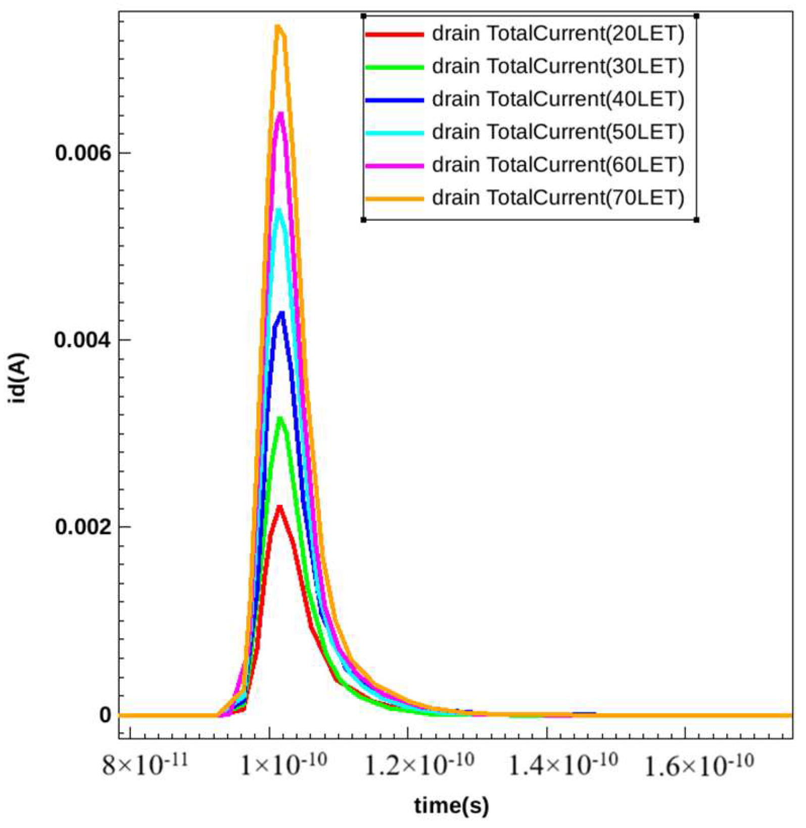
3.4. Analysis of the Change of Current Peak Value Caused by Different LET Incidence
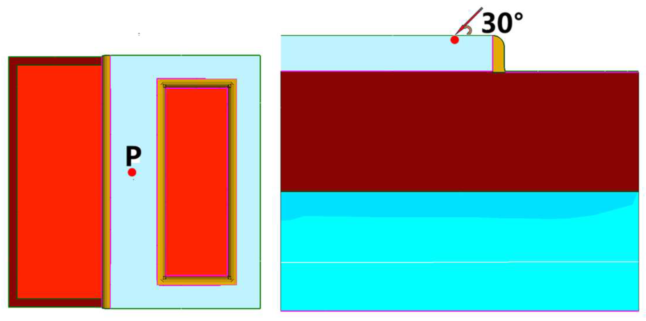
4. Analysis of the Impact Mechanism of Different Incident Positions on Single-Event Transients
5. Conclusions
Author Contributions
Funding
Institutional Review Board Statement
Informed Consent Statement
Data Availability Statement
Conflicts of Interest
References
- Wang, C. The influence with reliability of motional satellite by the single-event phenomena. Semicond. Intell. 1998, 35, 1–8. [Google Scholar]
- Chen, P. Radiation Effects on Semiconductor Devices and Integrated Circuits; National Defense Industry Press: Beijing, China, 2005. [Google Scholar]
- Johnston, A.H. Space radiation effects and reliability considerations for micro- and optoelectronic devices. IEEE Trans. Device Mater. Reliab. 2010, 10, 449–459. [Google Scholar] [CrossRef]
- Koons, H.C. The impact of the space environment on space systems. In Proceedings of the 6th Space Charging Technology Conference, Como, Italy, 5–9 October 1998. [Google Scholar]
- Tribble, A.C. The space environment and its impact on spacecraft design. In Proceedings of the AIAA Aerospace Sciences Meeting & Exhibit 31st AIAA Aerospace Sciences Meeting and Exhibit, Reno, NV, USA, 11–14 January 1993. [Google Scholar]
- Darrin, M.A.G. The impact of the space radiation environment on micro electro mechanical systems (MEMS) and microstructures. In Proceedings of the European Conference on Radiation & Its Effects on Components & Systems, Cap d’Agde, France, 23 September 2005. [Google Scholar] [CrossRef]
- Schott, J.U. Particle radiation effects in charge coupled devices (CCDs) with applications in single event experiments. In Proceedings of the RADECS 91 First European Conference on Radiation and its Effects on Devices and Systems, Montpellier, France, 9–12 September 1991; pp. 353–356. [Google Scholar] [CrossRef]
- Massengill, L.W.; Bhuva, B.L.; Holman, W.T.; Alles, M.L.; Loveless, T.D. Technology scaling and soft error reliability. In Proceedings of the 2012 IEEE International Reliability Physics Symposium (IRPS), Anaheim, CA, USA, 15–19 April 2012. [Google Scholar] [CrossRef]
- Huard, V. Technology scaling and reliability: Challenges and opportunities. In Proceedings of the 2015 IEEE International Electron Devices Meeting (IEDM), Washington, DC, USA, 7–9 December 2015. [Google Scholar] [CrossRef]
- DasGupta, S. Effect of well and substrate potential modulation on single event pulse shape in deep submicron CMOS. IEEE Trans. Nucl. Sci. 2007, 54, 2407–2412. [Google Scholar] [CrossRef]
- Gadlage, B.M. Comparison of heavy ion and proton induced combinatorial and sequential logic error rates in a deep submicron process. IEEE Trans. Nucl. Sci. 2005, 52, 2120. [Google Scholar] [CrossRef]
- Mahatme, N.N. Comparison of combinational and sequential error rates for a deep submicron process. IEEE Trans. Nucl. Sci. 2011, 58, 2719. [Google Scholar] [CrossRef]
- Li, D.M. Study of total ionizing dose radiation effects on enclosed gate transistors in a commercial CMOS technology. Chin. Phys. 2007, 16, 3760–3765. [Google Scholar]
- Vinogradov, S.M.; Atkin, E.V.; Ivanov, P.Y. Creating a parameterized model of a CMOS transistor with a gate of enclosed layout. J. Phys. Conf. Ser. 2016, 675, 042043. [Google Scholar]
- Kumar, A.; Shilla, P.; Kamal, Y. Study and Analysis of Enclosed Gate FET’s. IOP Conf. Ser. Mater. Sci. Eng. 2021, 1033, 012024. [Google Scholar] [CrossRef]
- Masalskii, N.V. Simulation of Silicon FETs with a Fully Enclosed Gate with a High-k Gate Dielectric. Russ. Microelectron. 2023, 52, 228–232. [Google Scholar] [CrossRef]
- Masalsky, N.V. CVC Simulation of Ultrathin Soi-Cmos Nanotransistors with a Fully Enclosed Gate. Russ. Microelectron. 2021, 50, 387–393. [Google Scholar] [CrossRef]
- SIilvestrl, M.; Gerardin, S.; Paccagnella, A. Degradation Induced by X-Ray Irradiation and Channel Hot Carrier Stresses in 130-nm NMOSFETs With Enclosed Layout. IEEE Trans. Nucl. Sci. 2008, 55, 3216–3223. [Google Scholar]
- Beznenova, V.; Michalowska-Forsyth, A. Aspect ratio of radiation-hardened MOS transistors Modelling of the equivalent channel dimensions of integrated MOS transistors in radiation-hardened enclosed layout. Elektrotechnik Informationstechnik 2018, 135, 61–68. [Google Scholar] [CrossRef]
- Lantz, M.D.; Galloway, K.F. Total Dose Effects on Circuit Speed Measurements. IEEE Trans. Nucl. Sci. 1983, 30, 4264–4269. [Google Scholar] [CrossRef]
- Platcheck, G.P.; Cardoso, G.S.; Balen, T.R. Pseudosymmetric Enclosed Layout Transistors for Radiation Hardened Analog Applications. IEEE Trans. Aerosp. Electron. Syst. 2023, 59, 2072–2076. [Google Scholar] [CrossRef]
- Platcheck, P.; Cardoso, G.S.; Balen, T.R. Behavioral and Variability Analysis of Enclosed Layout Transistors for Radiation Hardened Analog Circuits. In Proceedings of the 2024 IEEE 25th Latin American Test Symposium (LATS), Maceio, Brazil, 9–12 April 2024; pp. 1–6. [Google Scholar] [CrossRef]
- Adell, P. Analysis of single-event transients in analog circuits. IEEE Trans. Nucl. Sci. 2000, 47, 2616–2623. [Google Scholar] [CrossRef]
- Poivey, C. Development of a test methodology for single-event transients (SETs) in linear devices. IEEE Trans. Nucl. Sci. 2001, 48, 2180–2186. [Google Scholar] [CrossRef]
- Hirao, T. Studies of single-event transient current induced in GaAs and Si diodes by energetic heavy ions. Radiat. Phys. Chem. 2001, 60, 269–272. [Google Scholar] [CrossRef]
- Sternberg, A.L. Effect of amplifier parameters on single-event transients in an inverting operational amplifier. IEEE Trans. Nucl. Sci. 2002, 49, 1496–1501. [Google Scholar] [CrossRef]
- Adell, P.C. Single event transient effects in a voltage reference. Microelectron. Reliab. 2004, 45, 355–359. [Google Scholar] [CrossRef]
- Buchner, S.; Mcmorrow, D. Single-Event Transients in Bipolar Linear Integrated Circuits. IEEE Trans. Nucl. Sci. 2006, 53, 3079–3102. [Google Scholar]
- Nichols, D.K.; Coss, J.R. Heavy ion and proton induced single event transients in comparators. IEEE Trans. Nucl. Sci. 1996, 43, 2960–2967. [Google Scholar]
- Pimingstorfer, H.; Halama, S.; Selberherr, S. A TCAD Environment for Process and Process and Device Engineering. ICVC: International Conference on VLSI and CAD 2. 1991. Available online: https://www.iue.tuwien.ac.at/pdf/ib_1991/CP1991_Pimingstorfer_1.pdf (accessed on 2 April 2025).
- Odanaka, S. TCAD: CHALLENGED TO VIRTUAL PROCESS. ICVC Int. Conf. VLSI CAD 1995, 4, 197–202. [Google Scholar]
- Walton, A.J. Total TCAD strategy for DFM in IC technology development. IEE Proc. Sci. Meas. Technol. 1997, 144, 63–68. [Google Scholar]
- Biegel, B.A. Accuracy counts in modeling TCAD’s future. IEEE Potentials 2000, 19, 19–22. [Google Scholar]
- Dai, L. CMOS Integrated Circuit EDA Technology, 2nd ed.; China Machine Press: Beijing, China, 2022; p. 469. [Google Scholar]
- 55 nm Logic Low Leakage 1.2 V/1.8 V/2.5 V and Ultra Low Power 0.9 V/1.8 V/2.5 V RF Calibre LVS Release Note 2016.


| Part | Material (or Element) | Size (or Concentration) |
|---|---|---|
| Gate | Polysilicon | 55 nm |
| Source/Drain Doping | As | 2 × 1020 cm−3 |
| Spacer | Si3N4 | 10 nm |
| Gate Oxide | SiO2 | 1 nm |
| Channel Doping | B | 8.5 × 1017 cm−3 |
| Parameter | Value |
|---|---|
| Gate Bias Voltage (V) | 0 |
| Drain Bias Voltage (V) | 1 |
| LET(MeV·cm2/mg) | 20 |
| Heavy Particle Incident Angle (°) | 30 |
Disclaimer/Publisher’s Note: The statements, opinions and data contained in all publications are solely those of the individual author(s) and contributor(s) and not of MDPI and/or the editor(s). MDPI and/or the editor(s) disclaim responsibility for any injury to people or property resulting from any ideas, methods, instructions or products referred to in the content. |
© 2025 by the authors. Licensee MDPI, Basel, Switzerland. This article is an open access article distributed under the terms and conditions of the Creative Commons Attribution (CC BY) license (https://creativecommons.org/licenses/by/4.0/).
Share and Cite
Wang, Z.; Li, G.; Tang, M. Study on Single-Event Transient Hardness of Semi-Enclosed Gate NMOS. Appl. Sci. 2025, 15, 4023. https://doi.org/10.3390/app15074023
Wang Z, Li G, Tang M. Study on Single-Event Transient Hardness of Semi-Enclosed Gate NMOS. Applied Sciences. 2025; 15(7):4023. https://doi.org/10.3390/app15074023
Chicago/Turabian StyleWang, Zhuoxiang, Gang Li, and Minghua Tang. 2025. "Study on Single-Event Transient Hardness of Semi-Enclosed Gate NMOS" Applied Sciences 15, no. 7: 4023. https://doi.org/10.3390/app15074023
APA StyleWang, Z., Li, G., & Tang, M. (2025). Study on Single-Event Transient Hardness of Semi-Enclosed Gate NMOS. Applied Sciences, 15(7), 4023. https://doi.org/10.3390/app15074023