The Challenges of Advanced CMOS Process from 2D to 3D

 ,
,
Abstract
:1. Introduction
2. Lithography of Nano-Scaled Transistors
2.1. Challenges in ArF lithography with Multi-Patterning [12]
2.1.1. Overlay
2.1.2. Mask with Reticle Enhancement Techniques (RETs)
2.2. Challenges in EUV Lithography
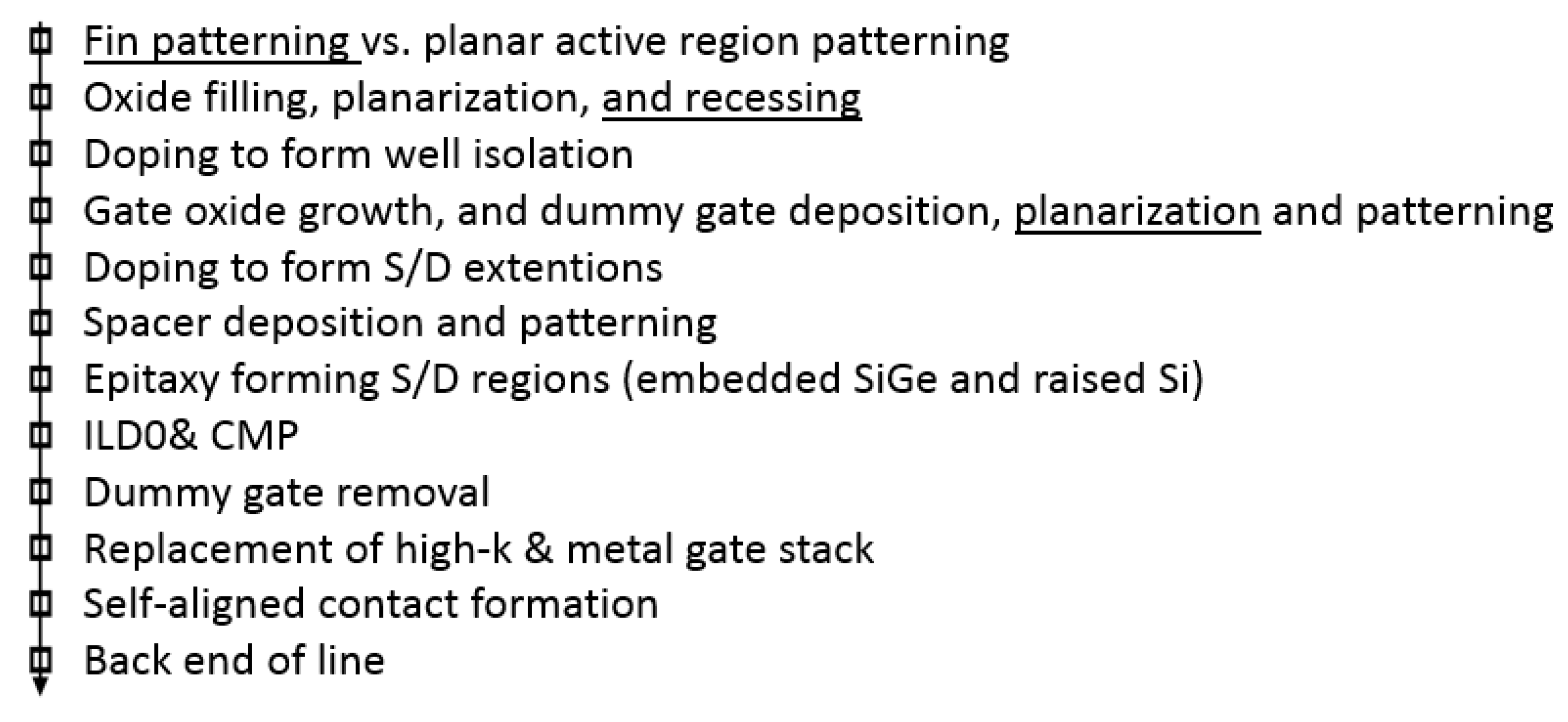
3. Process Integration of New Transistor Architecture
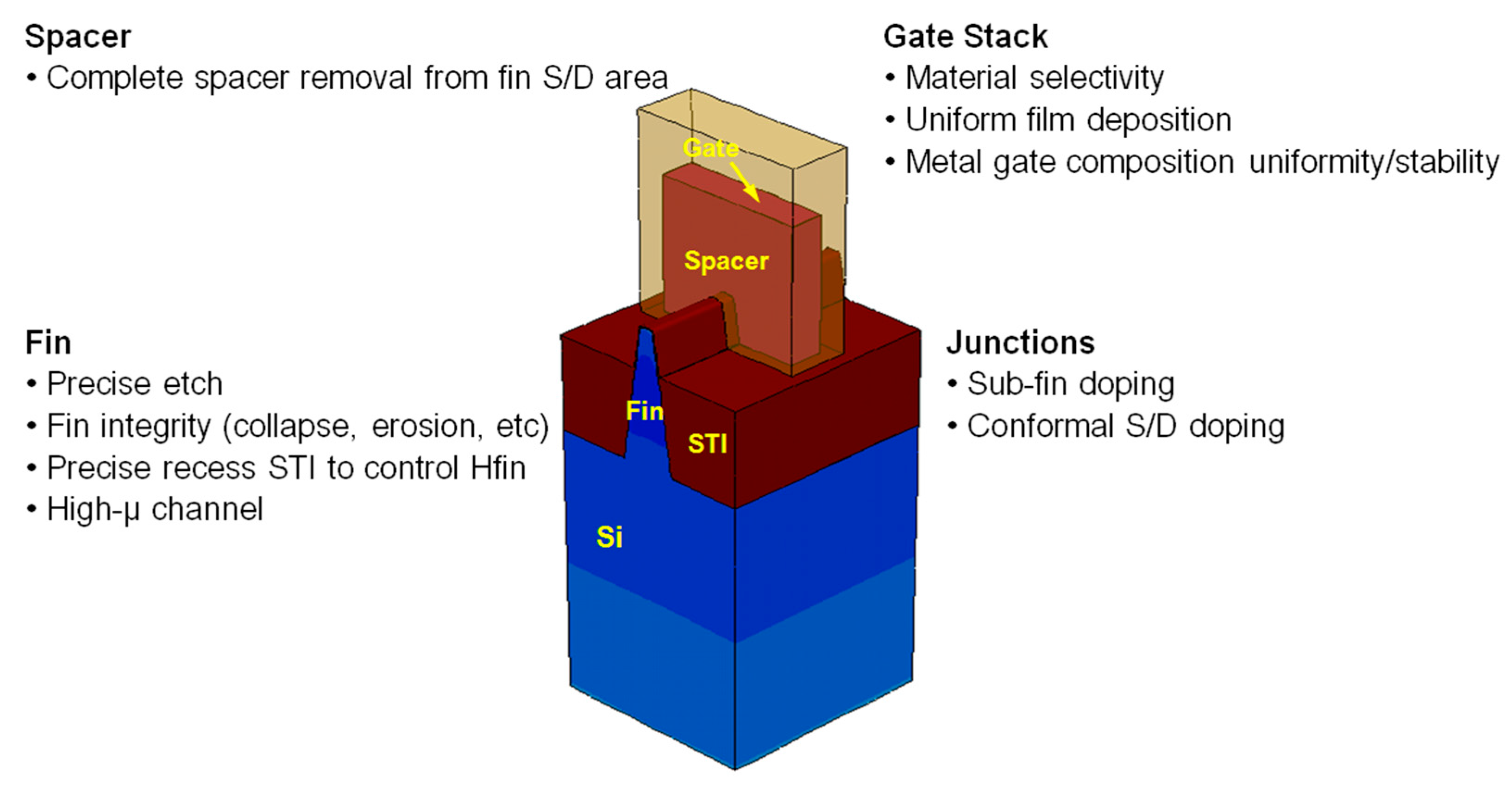
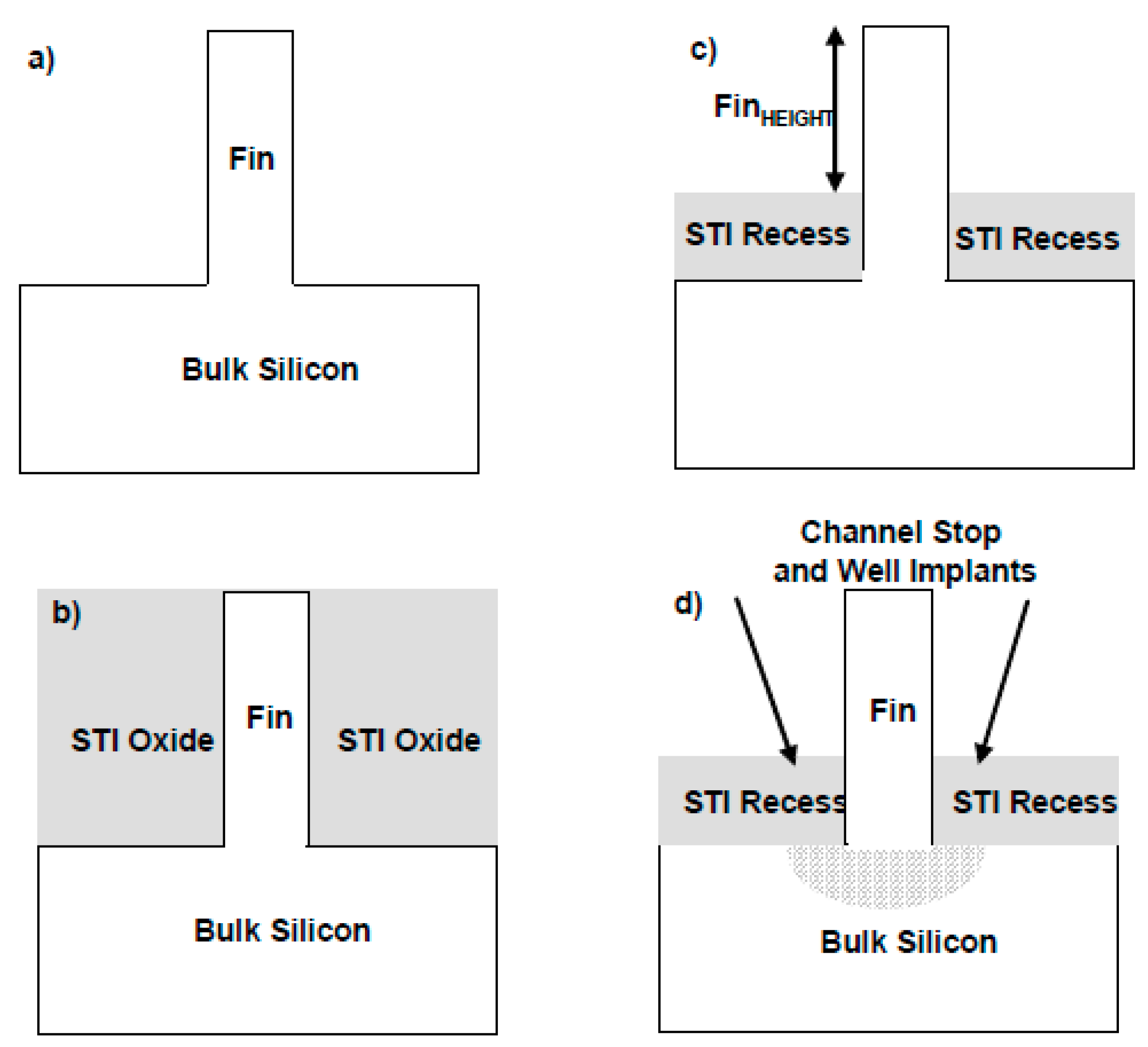
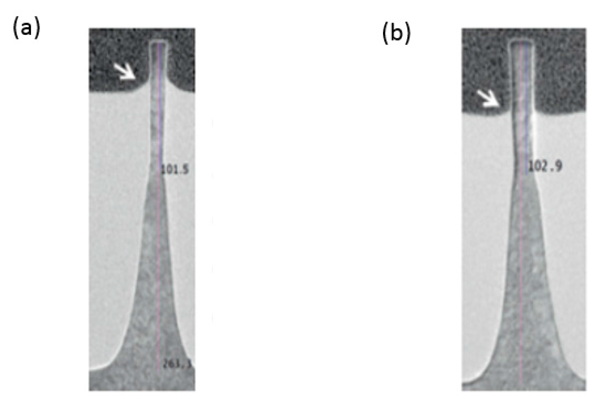
3.1. Precise and Uniform Fin Formation
3.2. 3D Gate and Spacer Patterning
3.3. Uniform Junction Formation in Fin
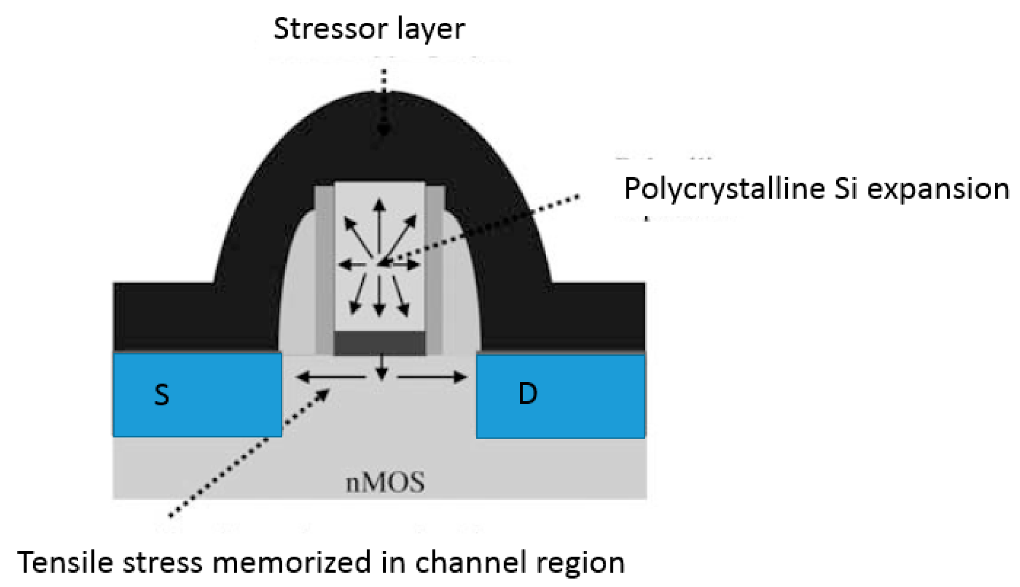
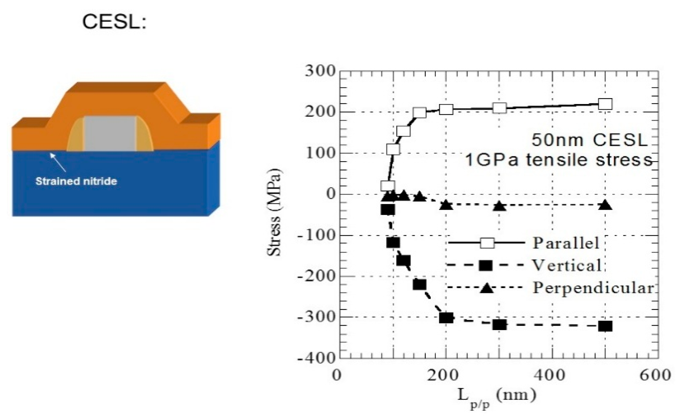
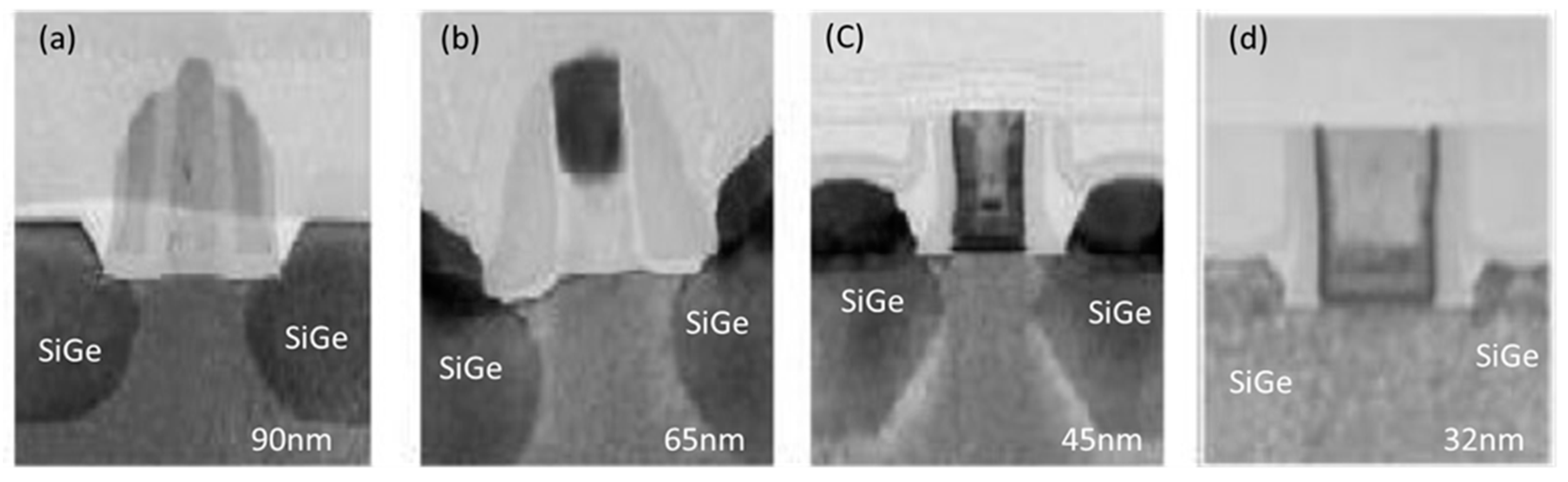
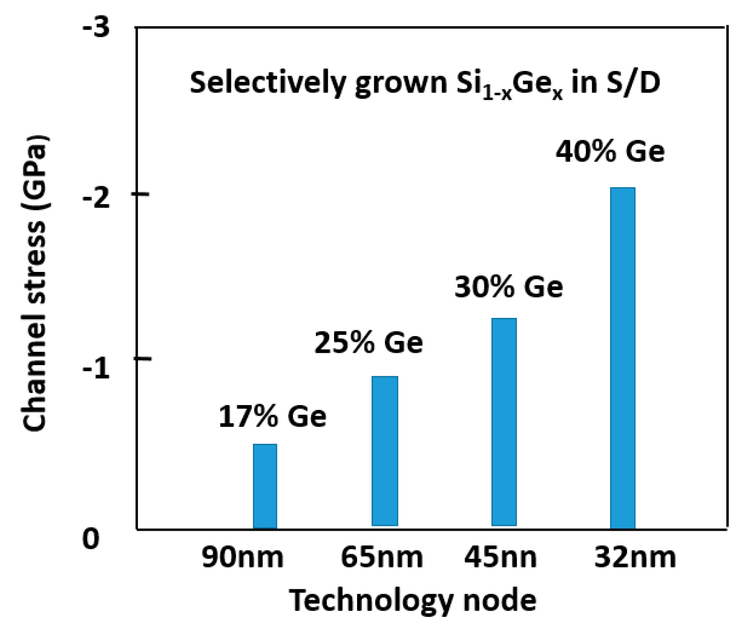
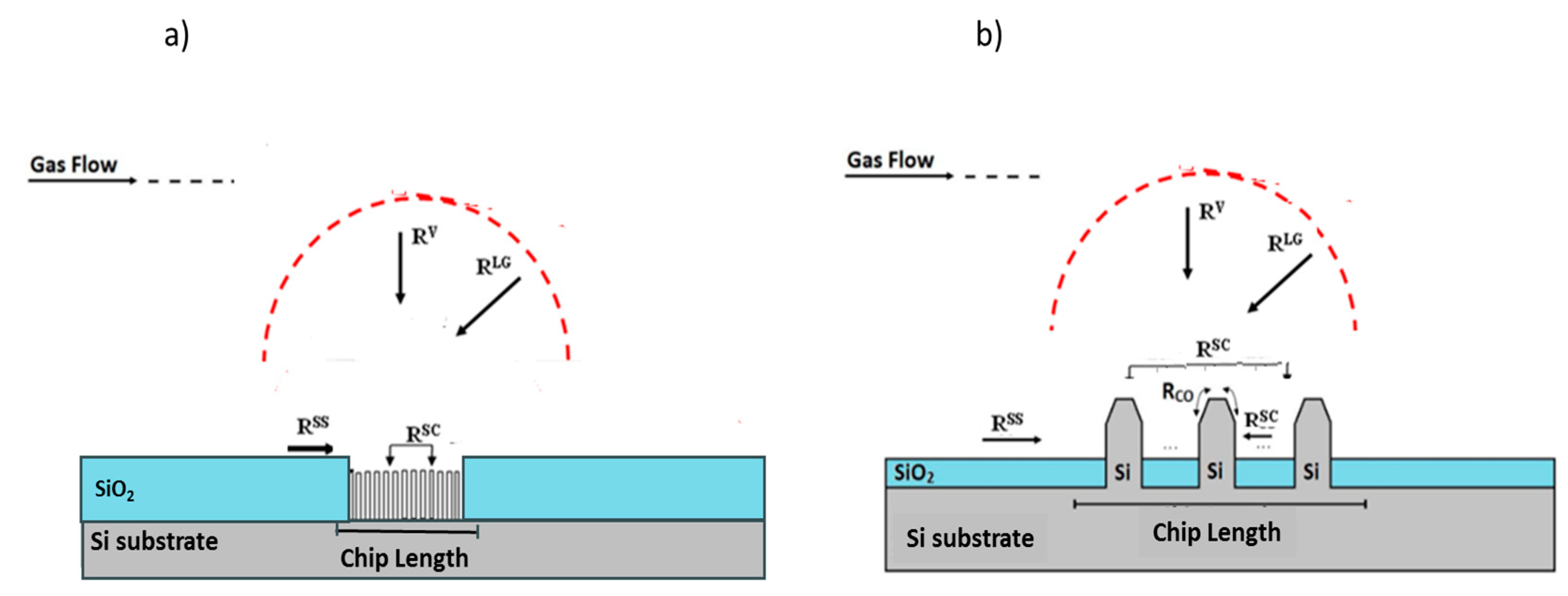
3.4. Stress Engineering
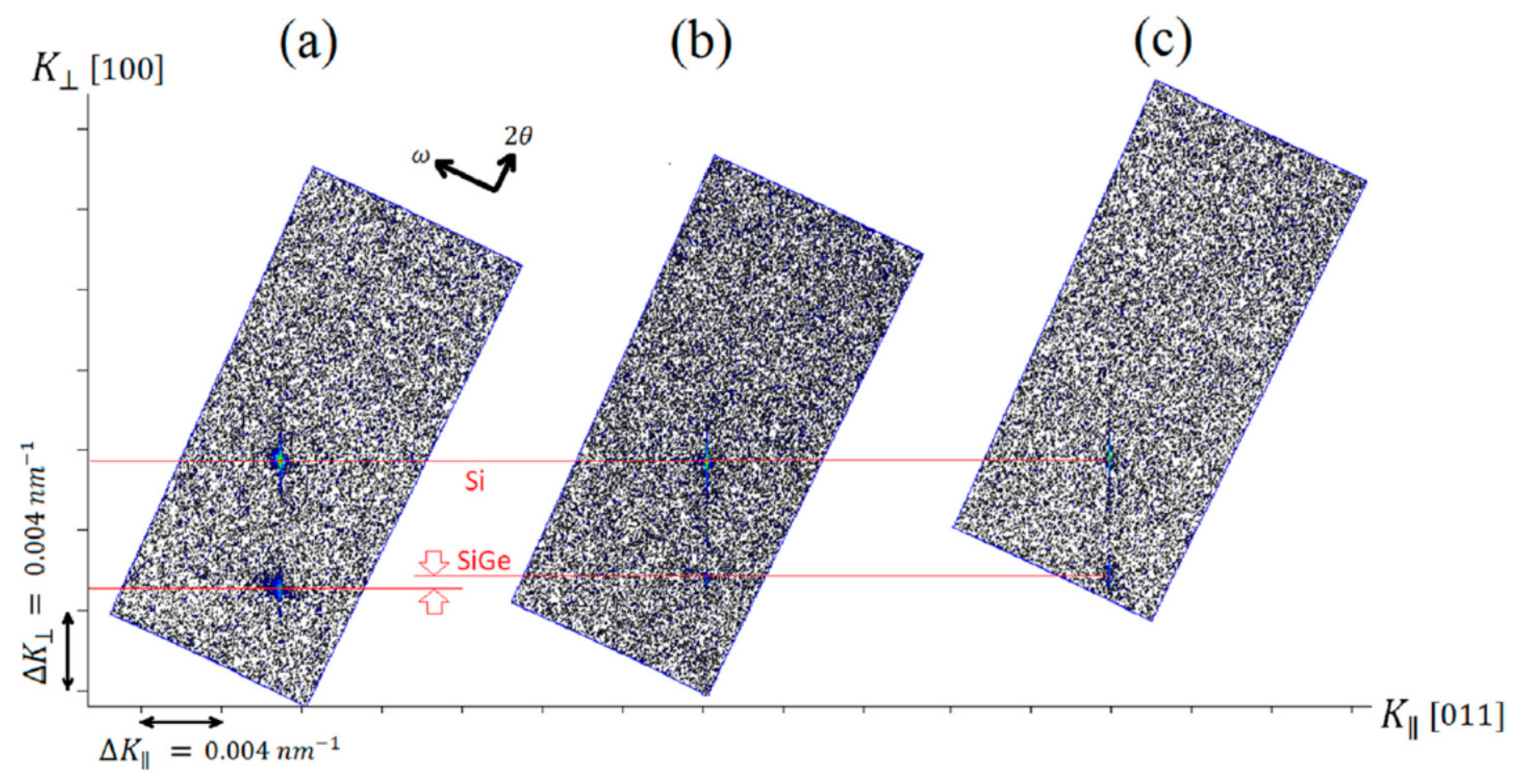
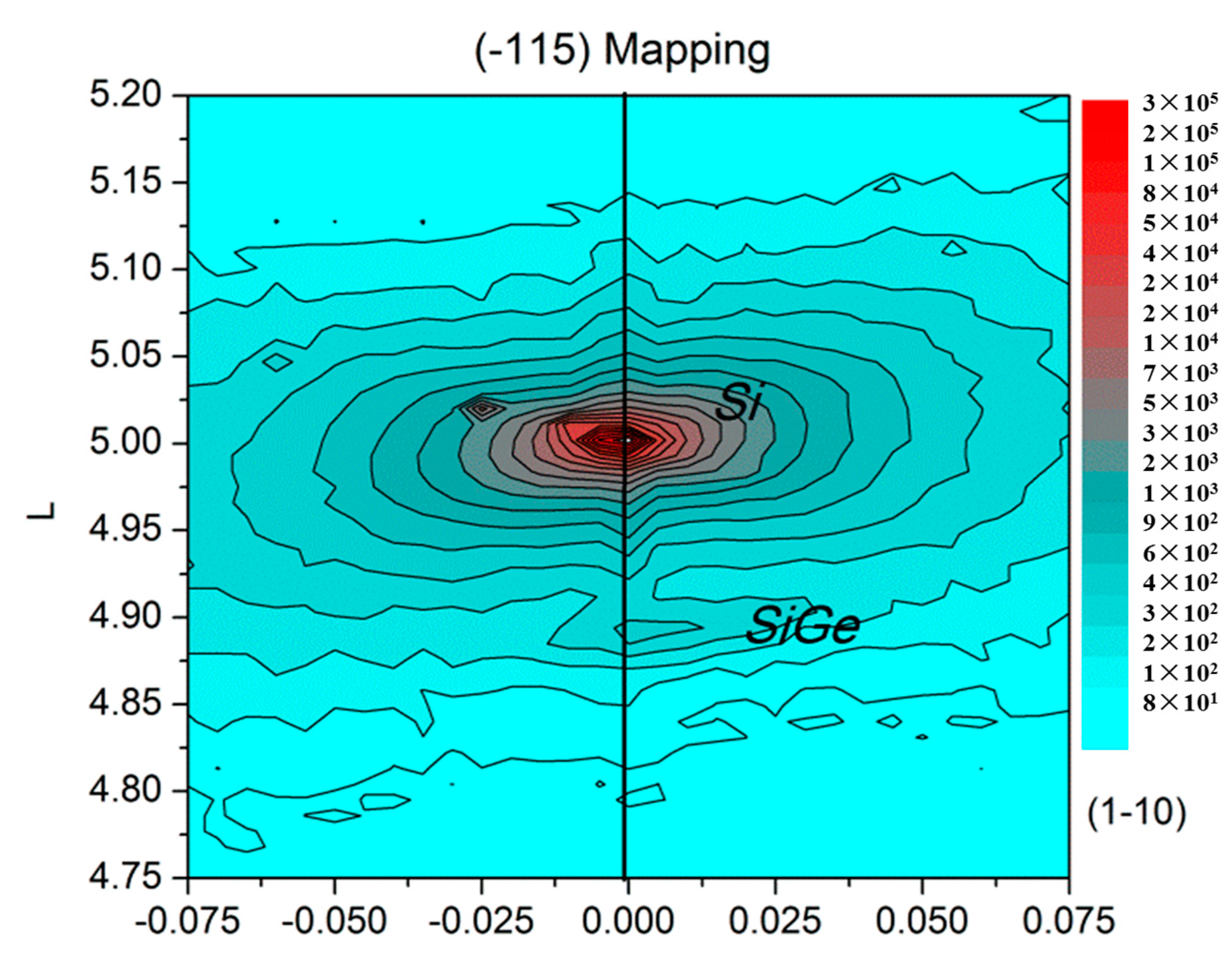
3.5. Stress Measurements in Nano-Scaled Transistors
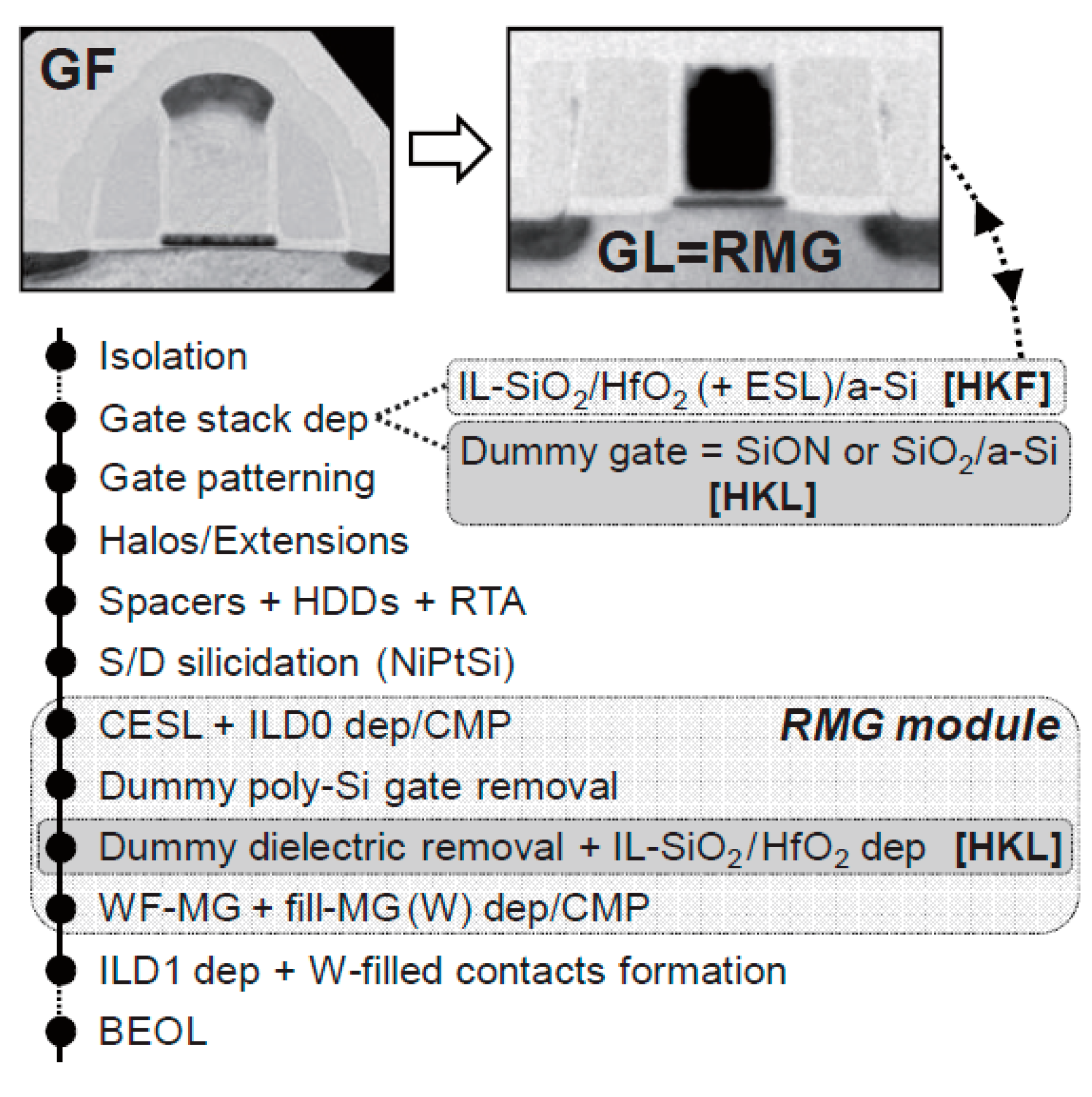
3.6. High-k Dielectric and Metal Gate (HKMG)
3.6.1. Evolution of HKMG
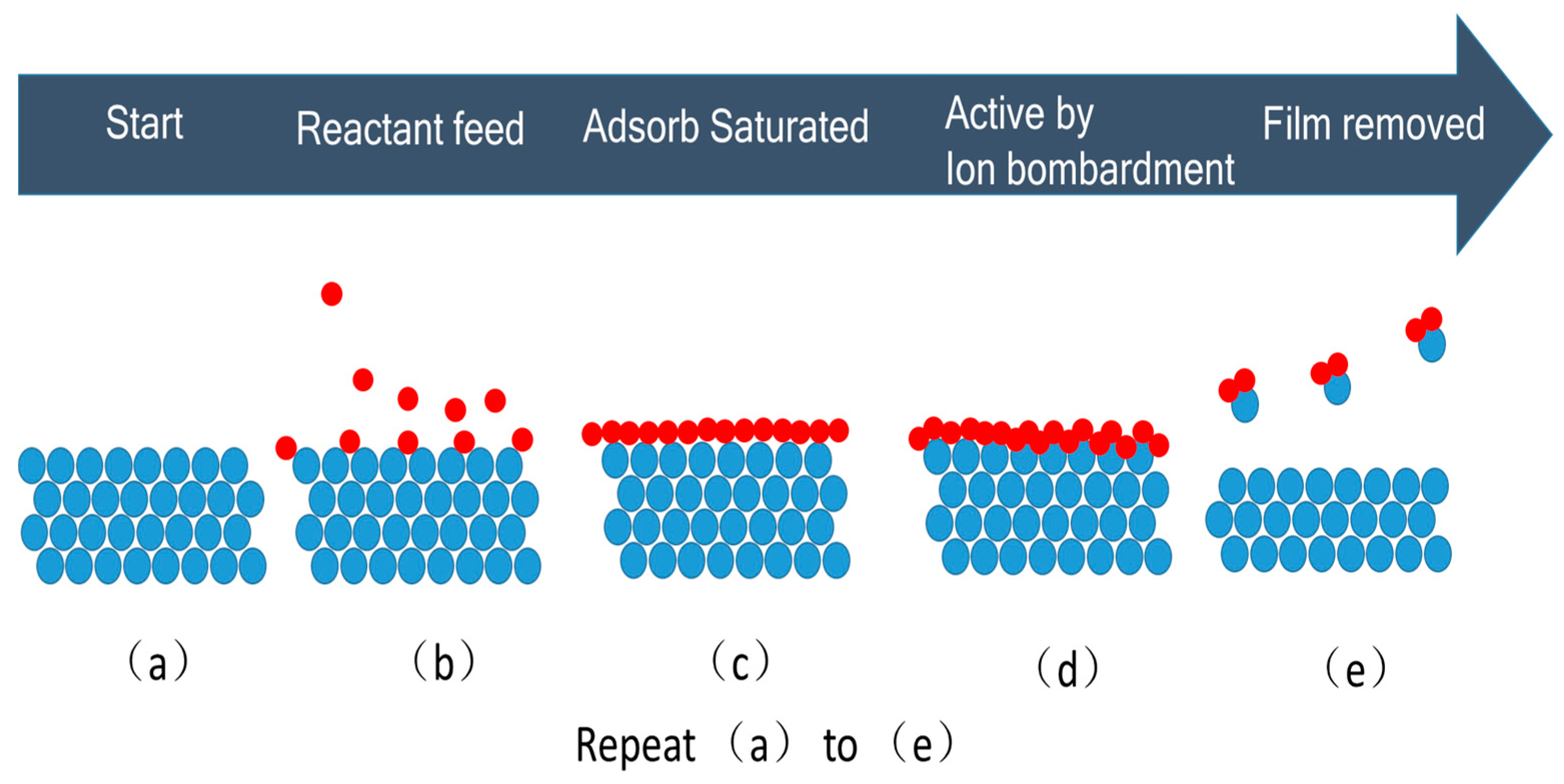
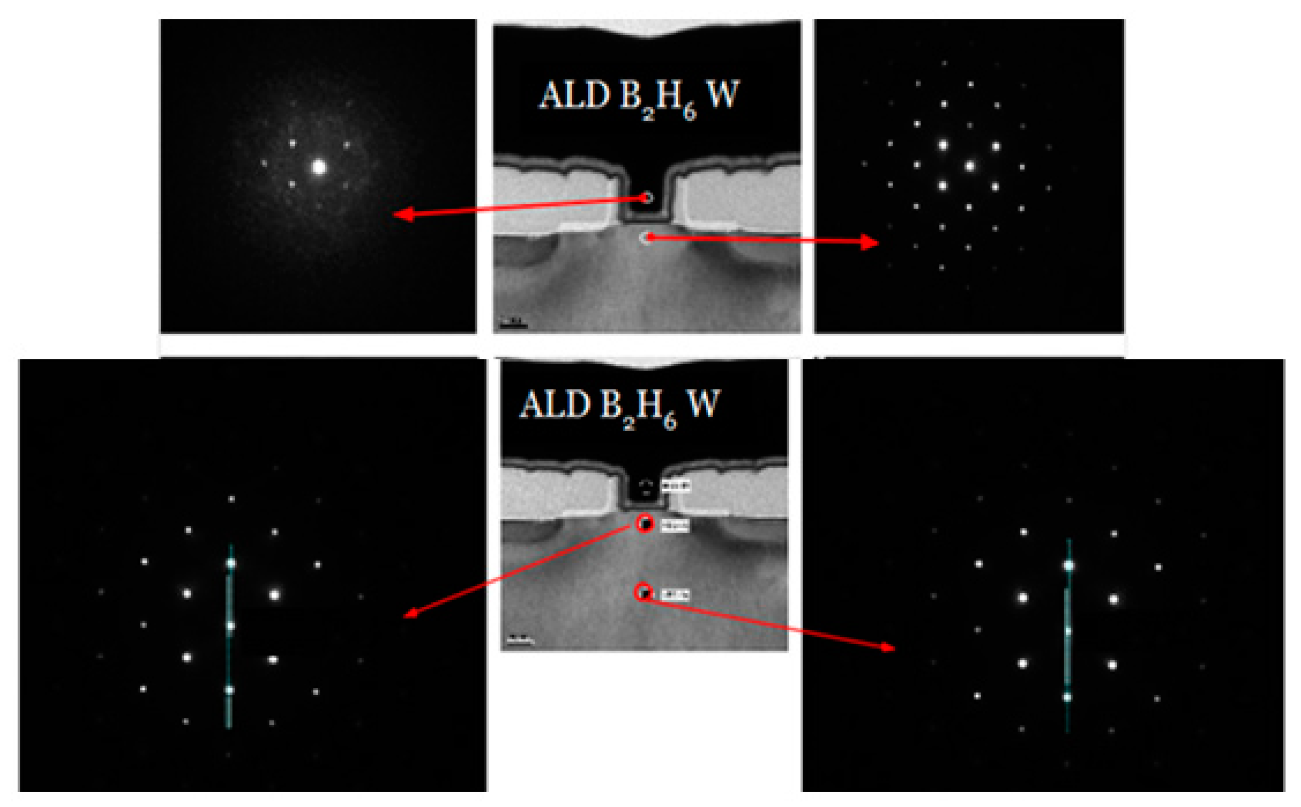
3.6.2. Atomic Layer Deposition of Metal Gate
3.7. Additional Sources of Variation
3.8. Common Challenges: Less Lateral Space Left
4. Dopant Implantation in CMOS
4.1. Challenge of Ion Implantation in 3D Structure Devices
4.1.1. Conformal Doping
4.1.2. Damage Control
5. The Etching Challenges and Solution of 3D
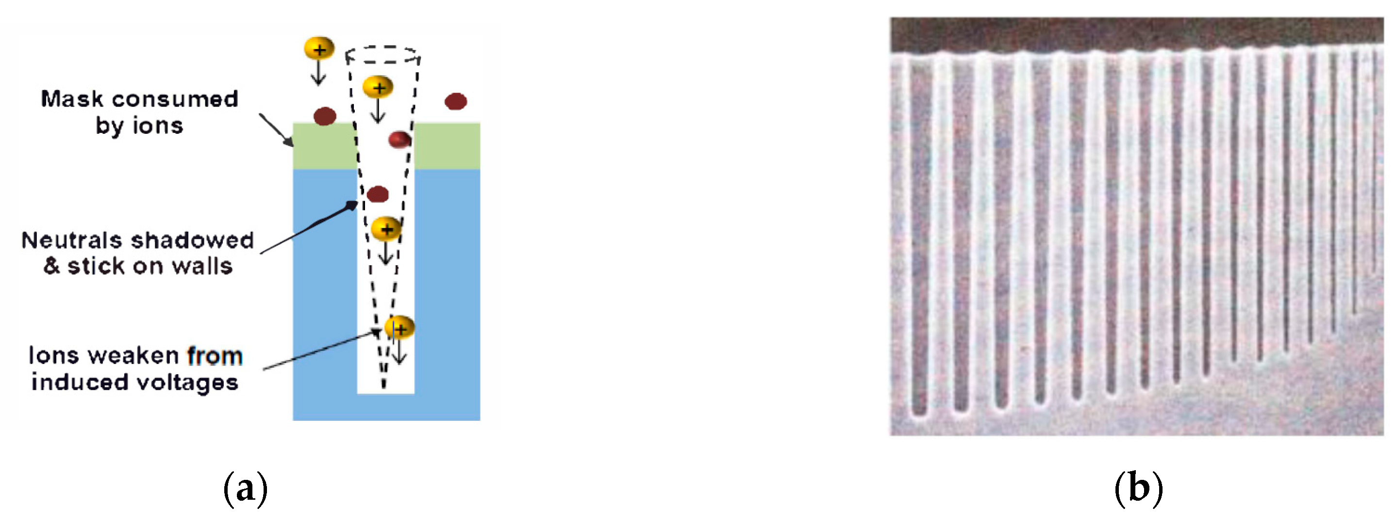
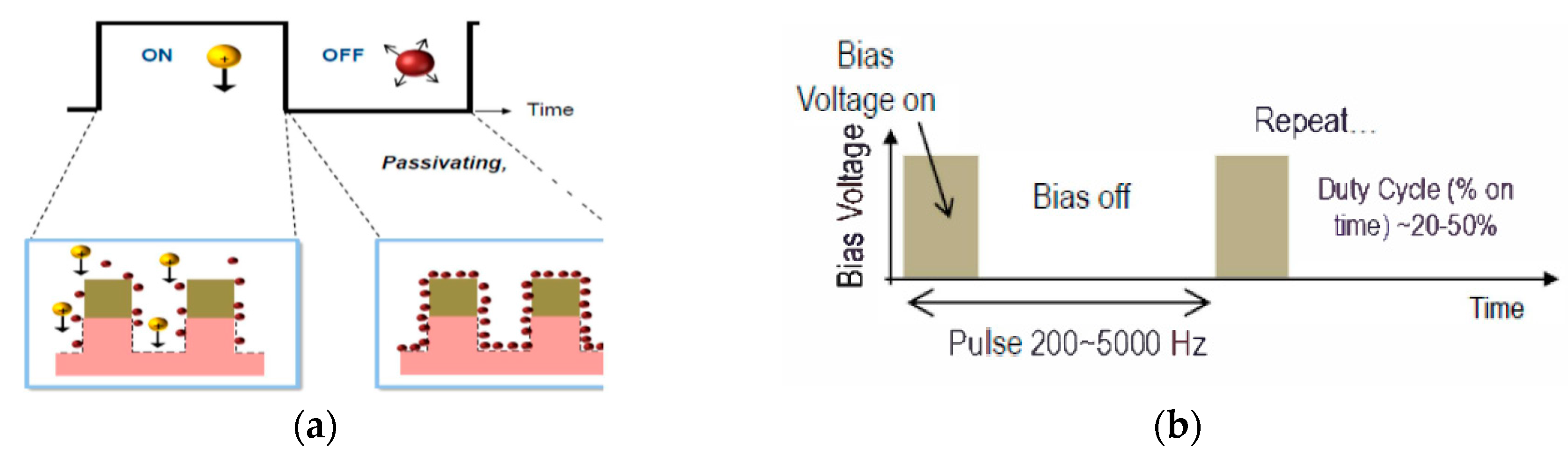
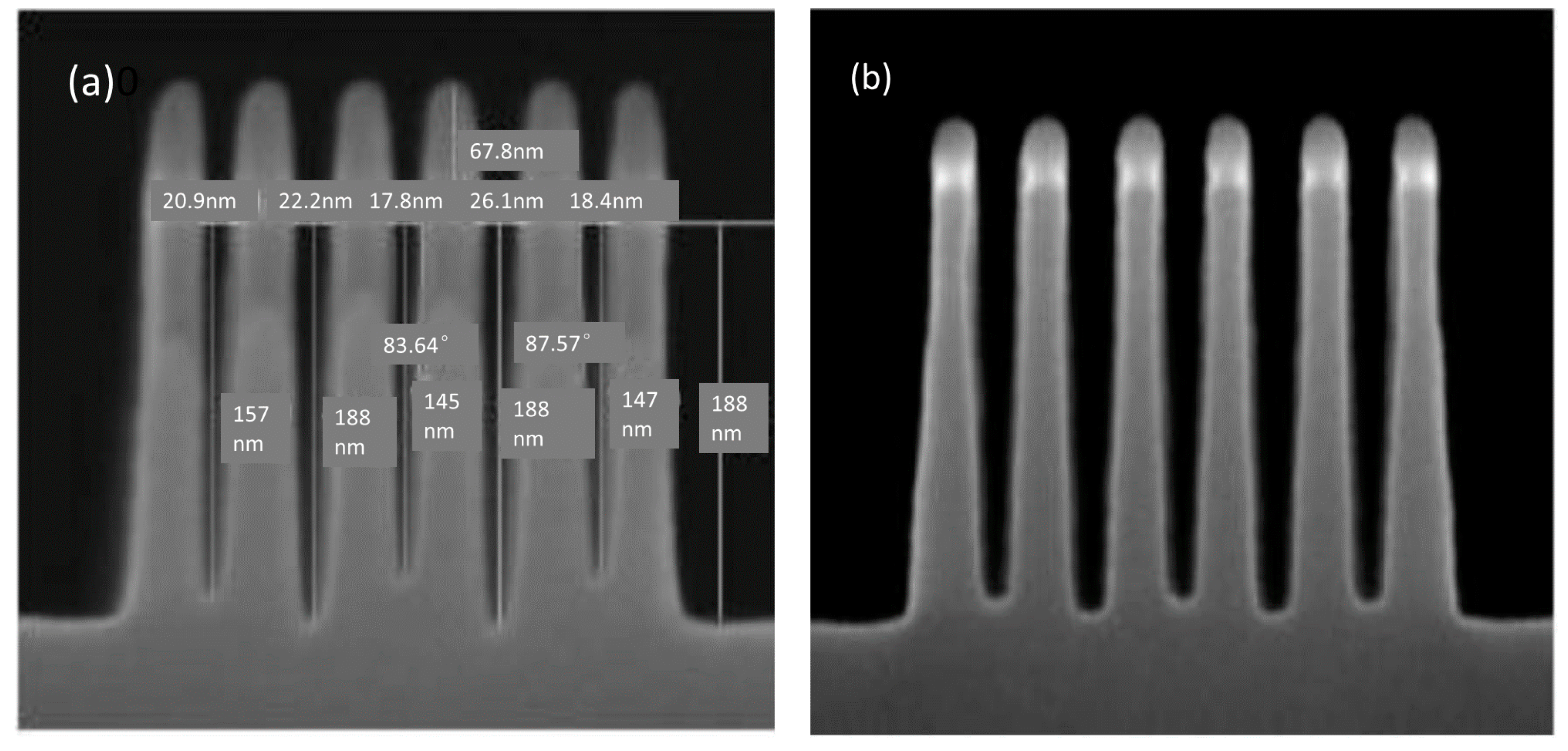
5.1. Depth Loading Control of Fin Etching
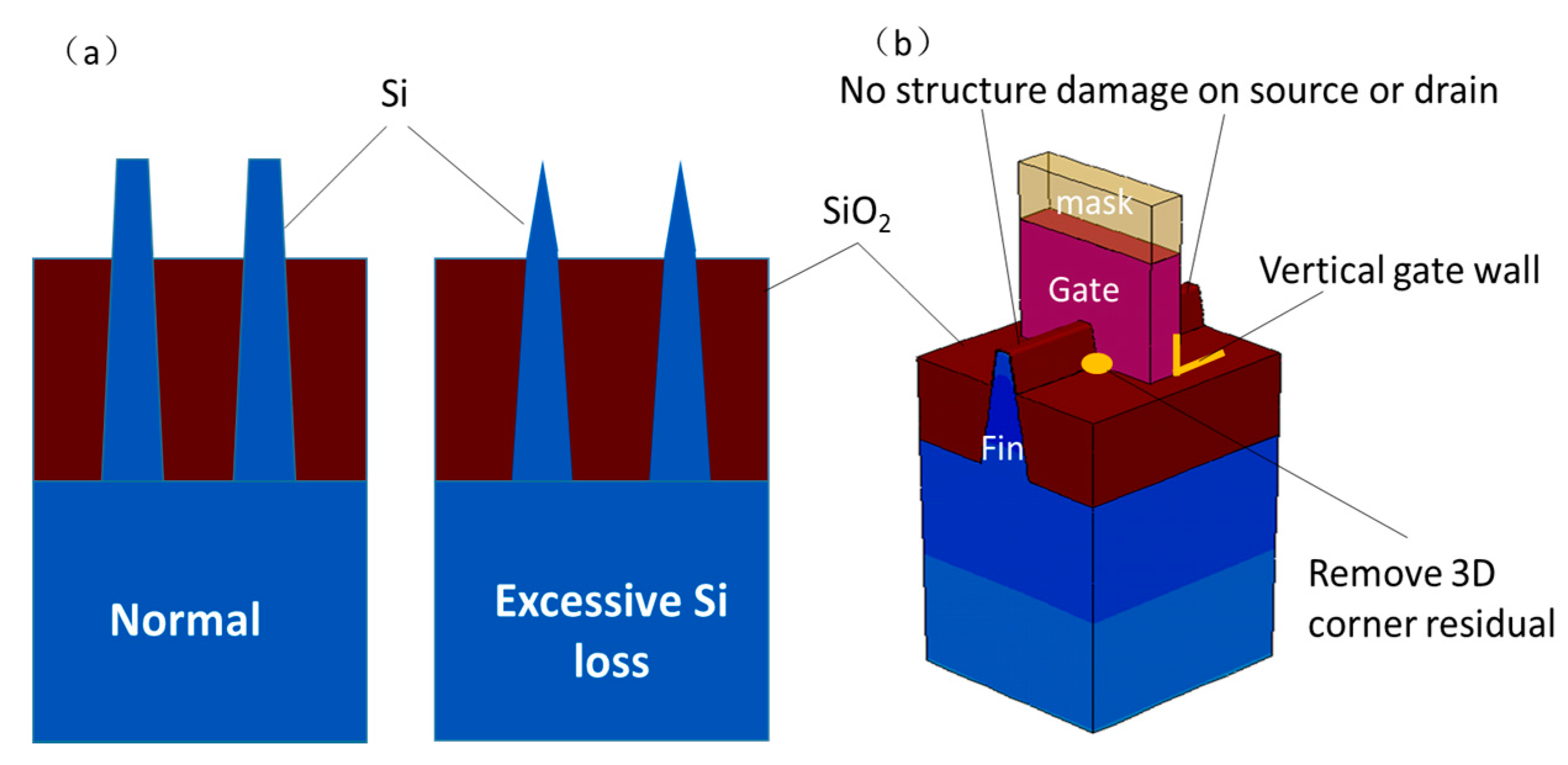
5.2. Gate Etching Control
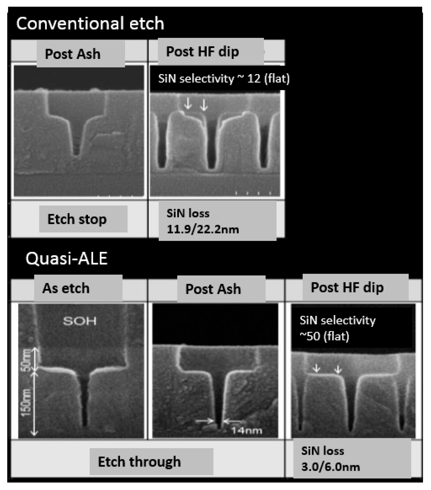
Self-Aligned Contact (SAC) Etching Selectivity Control
5.3. STI Process for the Gate
5.4. Gate Process
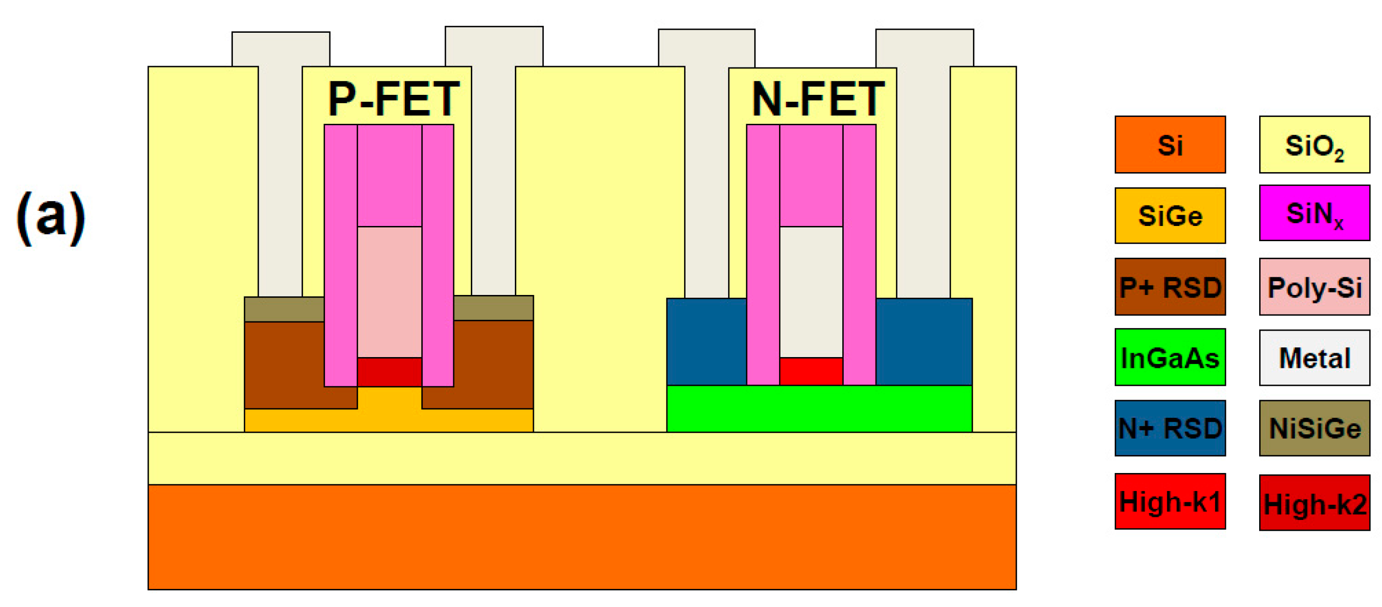
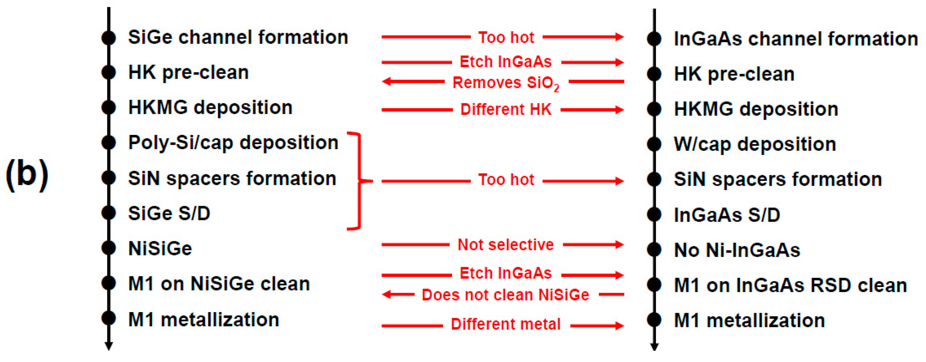
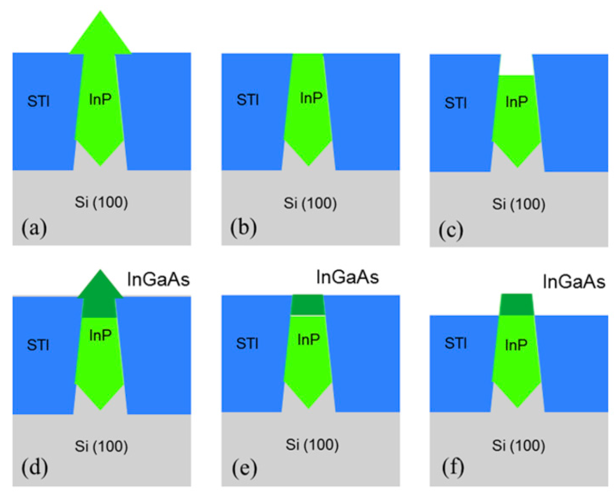
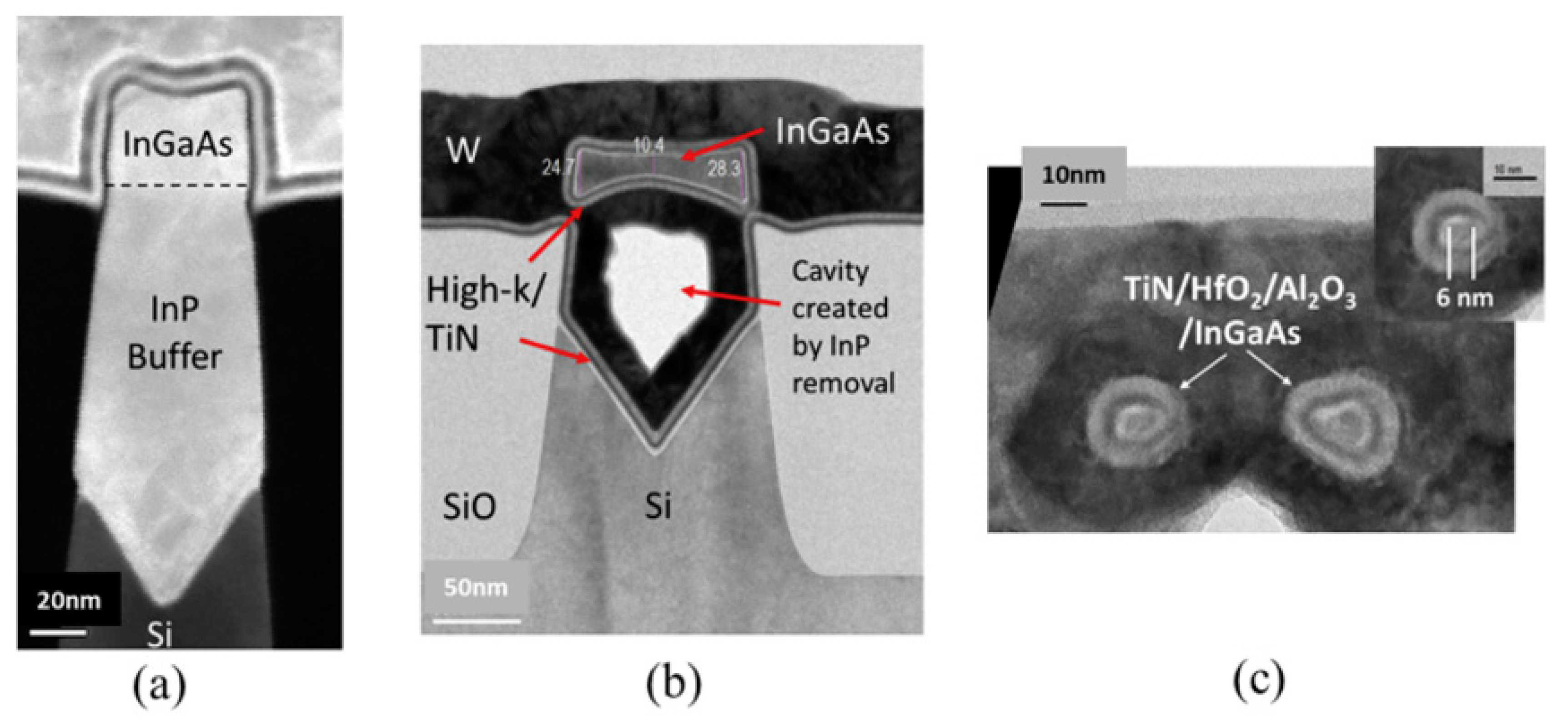
6. Challenges in Processing III-V 3D Transistor on Si
7. Challenges in Circuit Design
8. Conclusions
Acknowledgments
Conflicts of Interest
References
- Colinge, J.P. (Ed.) The SOI MOSFET: From Single Gate to Multigate. In FinFETs and Other Multi-Gate Transistors; Tyndall National Institute: Cork, Ireland, 2008; pp. 2–4. [Google Scholar]
- Soitec Official Website. Available online: https://www.soitec.com/en (accessed on 21 June 2017).
- Veloso, A.; Ragnarsson, L.Å.; Cho, M.J.; Devriendt, K.; Kellens, K.; Sebaai, F.; Suhard, S.; Brus, S.; Crabbe, Y.; Schram, T. Gate-last vs. gate-first technology for aggressively scaled EOT logic/RF CMOS. In Proceedings of the IEEE 2011 Symposium on VLSI Technology (VLSIT), Honolulu, HI, USA, 14–16 June 2011; pp. 34–35. [Google Scholar]
- Mertens, H.; Ritzenthaler, R.; Hikavyy, A.; Kim, M.S.; Tao, Z.; Wostyn, K.; Chew, S.A.; de Keersgieter, A.; Mannaert, G.; Rosseel, E.; et al. Gate-All-Around MOSFETs based on Vertically Stacked Horizontal Si Nanowires in a Replacement Metal Gate Process on Bulk Si Substrates. In Proceedings of the 2016 IEEE Symposium on VLSI Technology, Honolulu, HI, USA, 14–16 June 2016. [Google Scholar] [CrossRef]
- Leading at the Edge, Technology and Manufacturing Day (Intel). Available online: https://www.intc.com/default.aspx?SectionId=817fbab8-2828-44a2-91a0-f10cb8ac2b03&LanguageId=1&EventId=637d959b-e595–4f0e-843e-5ee9af9d6520 (accessed on 20 June 2017).
- IBM Research Alliance Builds New Transistor for 5 nm Technology (IBM). Available online: https://www-03.ibm.com/press/us/en/pressrelease/52531.wss (accessed on 20 June 2017).
- Kuhn, K.J. Considerations for Ultimate CMOS Scaling. IEEE Trans. Electron Devices 2012, 59, 1813–1828. [Google Scholar] [CrossRef]
- Pikus, F.G.; Torres, A. Advanced multi-patterning and hybrid lithography techniques. In Proceedings of the 2016 21st Asia and South Pacific Design Automation Conference (ASP-DAC), Macau, China, 25–28 January 2016. [Google Scholar] [CrossRef]
- Yaegashi, H. Pattern Fidelity control in Multi-patterning towards 7 nm node. In Proceedings of the 2016 IEEE 16th International Conference on Nanotechnology (IEEE-NANO), Sendai, Japan, 22–25 August 2016. [Google Scholar] [CrossRef]
- Jiang, J.; Chakrabarty, S.; Yu, M.; Ober, C.K. Metal oxide nanoparticle photoresists for EUV patterning. J. Photopolym. Sci. Technol. 2014, 27, 663–666. [Google Scholar] [CrossRef]
- Mulkens, J.; Hanna, M. Overlay and Edge Placement Control Strategies for the 7-nm node using EUV and ArF lithography. In Extreme Ultraviolet (EUV) Lithography VI; SPIE: San Jose, CA, USA, 2016; Volume 9422. [Google Scholar] [CrossRef]
- Wu, Q. Key points in 14 nm photolithographic process development, challenges and process window capability. In Proceedings of the 2017 China Semiconductor Technology International Conference (CSTIC), Shanghai, China, 12–13 March 2017. [Google Scholar] [CrossRef]
- Verstappen, L.; Mos, E. Holistic overlay control for multi patterning process layers at the 10 nm and 7 nm nodes. In Metrology, Inspection, and Process Control for Microlithography XXX; SPIE: San Jose, CA, USA, 2016; Volume 9778. [Google Scholar] [CrossRef]
- Pirati, A.; Peeters, R. EUV lithography performance for manufacturing: Status and outlook. In Extreme Ultraviolet (EUV) Lithography VII; SPIE: San Jose, CA, USA, 2016; Volume 9776. [Google Scholar] [CrossRef]
- Pirati, A.; Peeters, R. Performance overview and outlook of EUV lithography systems. In Extreme Ultraviolet (EUV) Lithography VI; SPIE: San Jose, CA, USA, 2016; Volume 9422. [Google Scholar] [CrossRef]
- Simone, D.D.; Mao, M. Metal Containing Resist Readiness for HVM EUV Lithography. J. Photopolym. Sci. Technol. 2016, 29, 501–507. [Google Scholar] [CrossRef]
- Mamezaki, D.; Watanabe, M. Development of the Transmittance Measurement for EUV Resist by Direct Resist Coating on a Photodiode. J. Photopolym. Sci. Technol. 2016, 29, 749–752. [Google Scholar] [CrossRef]
- Yoda, Y.; Hayakawa, A. Next-generation immersion scanner optimizing on-product performance for 7 nm node. In Optical Microlithography XXIX; SPIE: San Jose, CA, USA, 2016; Volume 9780. [Google Scholar] [CrossRef]
- Wojdyla, A.; Donoghue, A. Aerial imaging study of the mask-induced line-width roughness of EUV lithography masks. In Extreme Ultraviolet (EUV) Lithography VII; SPIE: San Jose, CA, USA, 2015; Volume 9776. [Google Scholar] [CrossRef]
- Antohe, A.O.; Balachandran, D. SEMATECH produces defect-free EUV mask blanks: Defect yield and immediate challenges. In Extreme Ultraviolet (EUV) Lithography VI; SPIE: San Jose, CA, USA, 2015; Volume 94221B. [Google Scholar] [CrossRef]
- Jan, C.-H.; Bhattacharya, U.; Brain, R.; Choi, S.-J.; Curello, G.; Gupta, G.; Hafez, W.; Jang, M.; Kang, M.; Komeyli, K.; et al. A 22 nm SoC Platform Technology Featuring 3-D Tri-Gate and High-k/Metal Gate, Optimized for Ultra Low Power, High Performance and High Density SoC Applications. In Proceedings of the 2012 IEEE International Electron Devices Meeting (IEDM), San Francisco, CA, USA, 10–13 December 2012; pp. 44–47. [Google Scholar]
- Jan, C.-H.; Agostinelli, M.; Buehler, M.; Chen, Z.-P.; Choi, S.-J.; Curello, G.; Deshpande, H.; Gannavaram, S.; Hafez, W.; Jalan, U.; et al. A 32 nm SoC Platform Technology with 2nd Generation High-k/Metal Gate Transistors Optimized for Ultra Low Power, High Performance, and High Density Product Applications. In Proceedings of the 2009 IEEE International Electron Devices Meeting (IEDM), Baltimore, MD, USA, 7–9 December 2009; pp. 647–650. [Google Scholar]
- Conley, A. FinFET vs. FD-SOI Key Advantages & Disadvantages. ChipEx 2014, 30 April 2014. [Google Scholar]
- Kuhn, K.J.; Murthy, A.; Kotlyar, R.; Kuhn, M. Past, Present and Future: SiGe and CMOS Transistor Scaling. ECS Trans. 2010, 33, 3–17. [Google Scholar]
- Kise, N.; Kinoshita, H.; Yukimachi, A.; Kanazawa, T.; Miyamoto, Y. Fin width dependence on gate controllability of InGaAs channel FinFETs with regrown source/drain. Solid-State Electron. 2016, 126, 92–95. [Google Scholar] [CrossRef]
- Jan, C.-H.; Al-Amoody, F.; Chang, H.-Y.; Chang, T.; Chen, Y.-W.; Dias, N.; Hafez, W.; Ingerly, D.; Jang, M.; Karl, E.; et al. A 14 nm SoC Platform Technology Featuring 2nd Generation Tri-Gate Transistors, 70 nm Gate Pitch, 52 nm Metal Pitch, and 0.0499 μm2 SRAM cells, Optimized for Low Power, High Performance and High Density SoC Products. In Proceedings of the 2015 Symposium on VLSI Technology (VLSI Technology), Kyoto, Japan, 16–18 June 2015; pp. T12–T13. [Google Scholar]
- Jacob, A.P.; Xie, R.; Sung, M.G.; Liebmann, L.; Lee, R.T.P.; Taylor, B. Scaling Challenges for Advanced CMOS Devices. Int. J. High Speed Electron. Syst. 2017, 26, 2–76. [Google Scholar] [CrossRef]
- Matsukawa, T.; Liu, Y.; Endo, K.; Ouchi, S.-I.; Masahara, M. Variability origins of FinFETs and perspective beyond 20 nm node. In Proceedings of the 2011 IEEE International SOI Conference (SOI), Tempe, AZ, USA, 3–6 October 2011. [Google Scholar] [CrossRef]
- Kavalieros, J.; Doyle, B.; Datta, S.; Dewey, G.; Doczy, M.; Jin, B.; Lionberger, D.; Metz, M.; Rachmady, W.; Radosavljevic, M. Tri-gate Transistor Architecture with High-k Gate Dielectrics, Metal Gates and Strain Engineering. In Proceedings of the 2006 Symposium on VLSI Technology, Digest of Technical Papers, Honolulu, HI, USA, 13–15 June 2006. [Google Scholar] [CrossRef]
- Kuhn, K.J. CMOS Transistor Scaling Past 32 nm and Implications on Variation. In Proceedings of the 2010 IEEE/SEMI Advanced Semiconductor Manufacturing Conference (ASMC), San Francisco, CA, USA, 11–13 July 2010. [Google Scholar] [CrossRef]
- Veloso, A.; De Keersgieter, A.; Matagne, P.; Horiguchi, N.; Collaert, N. Advances on doping strategies for triple-gate finFETs and lateral gate-all-around nanowire FETs and their impact on device performance. Mater. Sci. Semicond. Proc. 2017, 62, 2–12. [Google Scholar] [CrossRef]
- Current, M.I. Ion implantation of advanced silicon devices: Past, present and future. Mater. Sci. Semicond. Proc. 2017, 62, 13–22. [Google Scholar] [CrossRef]
- Ang, K.-W.; Barnett, J.; Loh, W.-Y.; Huang, J.; Min, B.-G.; Hung, P.Y.; Ok, I.; Yum, J.H.; Bersuker, G.; Rodgers, M.; et al. 300 mm FinFET results utilizing conformal, damage free, ultra shallow junctions (Xj∼5 nm) formed with molecular monolayer doping technique. In Proceedings of the 2011 IEEE International Electron Devices Meeting (IEDM), Washington, DC, USA, 5–7 December 2011; Volume 1–35, p. 35. [Google Scholar]
- Pidin, S.; Mori, T.; Inoue, K.; Fukuta, S.; Itoh, N.; Mutoh, E.; Ohkoshi, K.; Nakamura, R.; Kobayashi, K.; Kawamura, K.; et al. A novel strain enhanced CMOS architecture using selectively deposited high tensile and high compressive silicon nitride films. In Proceedings of the IEEE International Electron Devices Meeting, IEDM Technical Digest, San Francisco, CA, USA, 13–15 December 2004; pp. 213N–216N. [Google Scholar]
- Xu, N.; Ho, B.; Choi, M.; Moroz, V.; Liu, T.J.K. Effectiveness of stressors in aggressively scaled FinFETs. IEEE Trans. Electron Devices 2012, 59, 1592–1598. [Google Scholar] [CrossRef]
- Ghani, T.; Armstrong, M.; Auth, C.; Bost, M.; Charvat, P.; Glass, G.; Hoffmann, T.; Johnson, K.; Kenyon, C.; Klaus, J.; et al. A 90 nm high volume manufacturing logic technology featuring novel 45 nm gate length strained silicon CMOS transistors. In Proceedings of the IEEE International Electron Devices Meeting, IEDM ′03 Technical Digest, Washington, DC, USA, 8–10 December 2003. [Google Scholar]
- Auth, C.; Allen, C.; Blattner, A.; Bergstrom, D.; Brazier, M.; Bost, M.; Buehler, M.; Chikarmane, V.; Ghani, T.; Glassman, T. A 22 nm high performance and low-power CMOS technology featuring fully-depleted tri-gate transistors, self-aligned contacts and high density MIM capacitors. In Proceedings of the 2012 IEEE Symposium on VLSI Technology, Honolulu, HI, USA, 12–14 June 2012; pp. 131–132. [Google Scholar]
- Thompson, S.; Sun, G.; Wu, K.; Lim, J.; Nishida, T. Key differences for process-induced uniaxial vs. substrate-induced biaxial stressed Si and Ge channel MOSFETs. In Proceedings of the IEEE International Electron Devices Meeting, IEDM Technical Digest, San Francisco, CA, USA, 13–15 December 2004; pp. 221–224. [Google Scholar]
- Mistry, K.; Allen, C.; Auth, C.; Beattie, B.; Bergstrom, D.; Bost, M.; Brazier, M.; Buehler, M.; Cappellani, A.; Chau, R.; et al. A 45 nm logic technology with high-k+ metal gate transistors, strained silicon, 9 Cu interconnect layers, 193 nm dry patterning, and 100% Pb-free packaging. In Proceedings of the IEEE International Electron Devices Meeting (IEDM), Washington, DC, USA, 10–12 December 2007; pp. 247–250. [Google Scholar]
- Bohr, M.; Mistry, K. Intel’s Revolutionary 22 nm Transistor Technology. 2011. Available online: http://download.intel.com/newsroom/kits/22nm/pdfs/22nm-Details_Presentation.pdf (accessed on 2 October 2017).
- Ohta, H.; Kim, Y.; Shimamune, Y.; Sakuma, T.; Hatada, A.; Katakami, A.; Soeda, T.; Kawamura, K.; Kokura, H.; Morioka, H.; et al. High performance 30 nm gate bulk CMOS for 45 nm node with/spl Sigma/-shaped SiGe-SD. In Proceedings of the IEEE International Electron Devices Meeting, IEDM Technical Digest, Washington, DC, USA, 5 December 2005; pp. 247–250. [Google Scholar]
- Tamura, N.; Shimamune, Y. 45 nm CMOS technology with low temperature selective epitaxy of SiGe. Appl. Surf. Sci. 2008, 254, 6067–6071. [Google Scholar] [CrossRef]
- Qin, C.; Yin, H.; Wang, G.; Hong, P.; Ma, X.; Cui, H.; Lu, Y.; Meng, L.; Yin, H.; Zhong, H.; et al. Study of sigma-shaped source/drain recesses for embedded-SiGe pMOSFETs. Microelectron. Eng. 2017, 181, 22–28. [Google Scholar] [CrossRef]
- Xiao, H. 3D IC Devices. In Technologies, and Manufacturing; Society of Photo-Optical Instrumentation Engineers (SPIE): Bellingham, WA, USA, 2016. [Google Scholar]
- Dutartre, D.; Talbot, A.; Loubet, N. Facet propagation in Si and SiGe epitaxy or etching. ECS Trans. 2006, 3, 473–487. [Google Scholar]
- Mujumdar, S.; Maitra, K.; Datta, S. Layout-dependent strain optimization for p-channel trigate transistors. IEEE Trans. Electron Devices 2012, 59, 72–78. [Google Scholar] [CrossRef]
- Hållstedt, J.; Kolahdouz, M.; Ghandi, R.; Radamson, H.H.; Wise, R. Pattern dependency in selective epitaxy of B-doped SiGe layers for advanced metal oxide semiconductor field effect transistors. J. Appl. Phys. 2008, 103, 054907. [Google Scholar] [CrossRef]
- Kolahdouz, M.; Hållstedt, J.; Khatibi, A.; Östling, M.; Wise, R.; Riley, D.J.; Radamson, H.H. Comprehensive evaluation and study of pattern dependency behavior in selective epitaxial growth of B-doped SiGe layers. IEEE Trans. Nanotechnol. 2009, 8, 291–297. [Google Scholar] [CrossRef]
- Wang, G.; Moeen, M.; Abedin, A.; Xu, Y.; Luo, J.; Guo, Y.; Qin, C.; Tang, Z.; Yin, H.; Li, J.; et al. Impact of pattern dependency of SiGe layers grown selectively in source/drain on the performance of 22 nm node pMOSFETs. Solid-State Electron. 2015, 114, 43–48. [Google Scholar] [CrossRef]
- Qin, C.; Wang, G.; Kolahdouz, M.; Luo, J.; Yin, H.; Yang, P.; Radamson, H.H. Impact of pattern dependency of SiGe layers grown selectively in source/drain on the performance of 14 nm node FinFETs. Solid-State Electron. 2016, 124, 10–15. [Google Scholar] [CrossRef]
- Radamson, H.; Thylen, L. Monolithic Nanoscale Photonics-Electronics Integration in Silicon and Other Group IV Elements; Elsevier: San Diego, CA, USA, 2014. [Google Scholar]
- Wang, G.; Luo, J.; Liu, J.; Yang, T.; Xu, Y.; Li, J.; Yin, H.; Yan, J.; Zhu, H.; Zhao, C.; et al. pMOSFETs Featuring ALD W Filling Metal Using SiH4 and B2H6 Precursors in 22 nm Node CMOS Technology. Nanoscale Res. Lett. 2017, 12, 306. [Google Scholar] [CrossRef] [PubMed]
- Hansson, G.V.; Radamsson, H.H.; Ni, W.X. Strain and relaxation in Si-MBE structures studied by reciprocal space mapping using high resolution X-ray diffraction. J. Mater. Sci. Mater. Electron. 1995, 6, 292–297. [Google Scholar] [CrossRef]
- Wang, G.L.; Moeen, M.; Abedin, A.; Kolahdouz, M.; Luo, J.; Qin, C.L.; Zhu, H.L.; Yan, J.; Yin, H.; Li, J.; et al. Optimization of SiGe selective epitaxy for source/drain engineering in 22 nm node complementary metal-oxide semiconductor (CMOS). J. Appl. Phys. 2013, 114, 123511. [Google Scholar] [CrossRef]
- Radamson, H.H.; Joelsson, K.B.; Ni, W.-X.; Hultman, L.; Hansson, G.V. Characterization of highly boron-doped Si, Si1−xGex and Ge layers by high-resolution transmission electron microscopy. J. Cryst. Growth 1995, 157, 80–84. [Google Scholar] [CrossRef]
- Nur, O.; Willander, M.; Hultman, L.; Radamson, H.H.; Hansson, G.V. CoSi2/Si1−xGex/Si(001) heterostructures formed through different reaction routes: Silicidation-induced strain relaxation, defect formation, and interlayer diffusion. J. Appl. Phys. 1995, 78, 7063–7069. [Google Scholar] [CrossRef]
- Hallstedt, J.; Blomqvist, M.; Persson, P.O.A.; Hultman, L.; Radamson, H.H. The effect of carbon and germanium on phase transformation of nickel on Si1−x−yGexCy epitaxial layers. J. Appl. Phys. 2004, 95, 2397. [Google Scholar] [CrossRef]
- Takeuchi, H.; King, T.-J. Scaling limits of hafnium—Silicate films for gate-dielectric applications. Appl. Phys. Lett. 2003, 83, 788–790. [Google Scholar] [CrossRef]
- Seong, N.J.; Yoon, S.G.; Yeom, S.J.; Woo, H.K.; Kil, D.S.; Roh, J.S.; Sohn, H.C. Effect of nitrogen incorporation on improvement of leakage properties in high-k HfO2 capacitors treated by N2-plasma. Appl. Phys. Lett. 2005, 87, 132903. [Google Scholar] [CrossRef]
- Zhao, C.; Witters, T.; Brijs, B.; Bender, H.; Richard, O.; Caymax, M.; Heeg, T.; Schubert, J.; Afanas’ev, V.V.; Stesmans, A.; Schlom, D.G. Ternary rare-earth metal oxide high-k layers on silicon oxide. Appl. Phys. Lett. 2005, 86, 132903. [Google Scholar] [CrossRef] [Green Version]
- Barlage, D.; Arghavani, R.; Dewey, G.; Doczy, M.; Doyle, B.; Kavalieros, J.; Murthy, A.; Roberds, B.; Stokley, P.; Chau, R. High-frequency response of 100 nm integrated CMOS transistors with high-k gate dielectrics. In Proceedings of the IEEE International Electron Devices Meeting, Washington, DC, USA, 2–5 December 2001. [Google Scholar]
- Robertson, J. Band offsets of wide-band-gap oxides and implications for future electronic devices. J. Vac. Sci. Technol. B Microelectron. Nanom. Struct. Proc. Meas. Phenom. 2000, 18, 1785–1791. [Google Scholar] [CrossRef]
- Brar, B.; Wilk, G.D.; Seabaugh, A.C. Direct extraction of the electron tunneling effective mass in ultrathin SiO2. Appl. Phys. Lett. 1996, 69, 2728–2730. [Google Scholar] [CrossRef]
- Vogel, E.M.; Ahmed, K.Z.; Hornung, B.; Henson, W.K.; McLarty, P.K.; Lucovsky, G.; Hauser, J.R.; Wortman, J.J. Modeled tunnel currents for high dielectric constant dielectrics. IEEE Trans. Electron Devices 1998, 45, 1350–1355. [Google Scholar] [CrossRef]
- Johansson, M.; Yousif, M.Y.A.; Lundgren, P.; Bengtsson, S.; Sundqvist, J.; Hårsta, A.; Radamson, H.H. HfO2 gate dielectrics on strained-Si and strained-SiGe layers. Semicond. Sci. Technol. 2003, 18, 820. [Google Scholar] [CrossRef]
- Choi, J.H.; Mao, Y.; Chang, J.P. Development of hafnium based high-k materials—A review. Mater. Sci. Eng. R Rep. 2011, 72, 97–136. [Google Scholar] [CrossRef]
- Zheng, Y.B.; Wang, S.J.; Huan, C.H.A. Microstructure-dependent band structure of HfO2 thin films. Thin Solid Films 2006, 504, 197–200. [Google Scholar] [CrossRef]
- Hwang, W.S.; Shen, C.; Wang, X.; Chan, D.S.H.; Cho, B.J. A Novel Hafnium Carbide HfCx Metal Gate Electrode for NMOS Device Application. In Proceedings of the IEEE Symposium on VLSI Technology, Kyoto, Japan, 12–14 June 2007; pp. 156–157. [Google Scholar]
- Wilk, G.D.; Wallace, R.M.; Anthony, J.M. High-k gate dielectrics: Current status and materials properties considerations. J. Appl. Phys. 2001, 89, 5243–5275. [Google Scholar] [CrossRef]
- Robertson, J. High dielectric constant gate oxides for metal oxide Si transistors. Rep. Prog. Phys. 2006, 69, 327–396. [Google Scholar] [CrossRef]
- Xiong, K.; Peacock, P.W.; Robertson, J. Fermi level pinning and Hf–Si bonds at HfO2: Polycrystalline silicon gate electrode interfaces. Appl. Phys. Lett. 2005, 86, 012904. [Google Scholar] [CrossRef]
- Hobbs, C.C.; Fonseca, L.R.C.; Knizhnik, A.; Dhandapani, V.; Samavedam, S.B.; Taylor, W.J.; Grant, J.M.; Dip, L.G.; Triyoso, D.H.; Hegde, R.I.; et al. Fermi-level pinning at the polysilicon/metal oxide interface-Part I. IEEE Trans. Electron Devices 2004, 51, 971–977. [Google Scholar] [CrossRef]
- George, S.M. Atomic Layer Deposition: An Overview. Chem. Rev. 2010, 110, 111–131. [Google Scholar] [CrossRef] [PubMed]
- Puurunen, R.L. Surface chemistry of atomic layer deposition: A case study for the trimethylaluminum/water process. J. Appl. Phys. 2005, 97, 121301. [Google Scholar] [CrossRef]
- Heo, S.C.; Choi, C. Plasma atomic layer deposited TiN metal gate for three dimensional device applications: Deposition temperature, capping metal and post annealing. Microelectron. Eng. 2012, 94, 11–13. [Google Scholar] [CrossRef]
- Jeon, S.; Park, S. Fabrication of Robust Triple- Ti1−xAlxN Metal Gate by Atomic Layer Deposition. J. Electrochem. Soc. 2010, 157, H1101–H1105. [Google Scholar] [CrossRef]
- Lee, A.; Fuchigami, N.; Pisharoty, D.; Hong, Z.; Haywood, E.; Joshi, A.; Mujumdar, S.; Bodke, A.; Karlsson, O.; Kim, H.; et al. Atomic layer deposition of HfxAlyCz as a work function material in metal gate MOS devices. J. Vac. Sci. Technol. A 2014, 32, 01A118. [Google Scholar] [CrossRef]
- Dekkers, H.F.W.; Lima, L.P.B.; Van Elshocht, S. Conductivity Improvements of Atomic Layer Deposited Ta3N5. ECS Trans. 2013, 58, 195–202. [Google Scholar] [CrossRef]
- Ragnarsson, L.A.; Chew, S.A.; Dekkers, H.; Luque, M.T.; Parvais, B.; De Keersgieter, A.; Devriendt, K.; Van Ammel, A.; Schram, T.; Yoshida, N.; et al. Highly scalable bulk FinFET Devices with Multi-VT options by conductive metal gate stack tuning for the 10-nm node and beyond. In Proceedings of the 2014 Symposium on VLSI Technology (VLSI-Technology): Digest of Technical Papers, Honolulu, HI, USA, 9–12 June 2014; pp. 1–2. [Google Scholar]
- Cho, G.H.; Rhee, S.W. Plasma-Enhanced Atomic Layer Deposition of TaCxNy Films with tert-Butylimido Tris-diethylamido Tantalum and Methane/Hydrogen Gas. Electrochem. Solid-State Lett. 2010, 13, H426–H427. [Google Scholar] [CrossRef]
- Triyoso, D.H.; Gregory, R.; Schaeffer, J.K.; Werho, D.; Li, D.; Marcus, S.; Wilk, G.D. Atomic layer deposited TaCy metal gates: Impact on microstructure, electrical properties, and work function on HfO2 high-k dielectrics. J. Appl. Phys. 2007, 102, 104509. [Google Scholar] [CrossRef]
- Xiang, J.; Zhang, Y.; Li, T.; Wang, X.; Gao, J.; Yin, H.; Li, J.; Wang, W.; Ding, Y.; Xu, C.; et al. Investigation of thermal atomic layer deposited TiAlX (X = N or C) film as metal gate. Solid-State Electron. 2016, 122, 64–69. [Google Scholar] [CrossRef]
- Xiang, J.; Li, T.; Zhang, Y.; Wang, X.; Gao, J.; Cui, H.; Yin, H.; Li, J.; Wang, W.; Ding, Y.; et al. Investigation of TiAlC by Atomic Layer Deposition as N Type Work Function Metal for FinFET. ECS J. Solid State Sci. Technol. 2015, 4, 441–444. [Google Scholar] [CrossRef]
- Xiang, J.; Ding, Y.; Du, L.; Xu, C.; Li, T.; Wang, X.; Li, J.; Zhao, C. Investigation of N Type Metal TiAlC by Thermal Atomic Layer Deposition Using TiCl4 and TEA as Precursors. ECS J. Solid State Sci. Technol. 2016, 5, 299–303. [Google Scholar] [CrossRef]
- Xiang, J.; Li, T.; Wang, X.; Du, L.; Ding, Y.; Wang, W.; Li, J.; Zhao, C. Thermal Atomic Layer Deposition of TaAlC with TaCl5 and TMA as Precursors. ECS J. Solid State Sci. Technol. 2016, 5, 633–636. [Google Scholar] [CrossRef]
- Xiang, J.; Wang, X.; Li, T.; Gao, J.; Han, K.; Yu, J.; Wang, W.; Li, J.; Zhao, C. Investigation of Thermal Atomic Layer Deposited TaAlC with Low Effective Work-Function on HfO2 Dielectric Using TaCl5 and TEA as Precursors. ECS J. Solid State Sci. Technol. 2017, 6, 38–41. [Google Scholar] [CrossRef]
- Wang, G.; Xu, Q.; Yang, T.; Xiang, J.; Xu, J.; Gao, J.; Li, C.; Li, J.; Yan, J.; Chen, D.; et al. Application of atomic layer deposition tungsten (ALD W) as gate filling metal for 22 nm and beyond nodes CMOS technology. ECS J. Solid State Sci. Technol. 2014, 3, 82–85. [Google Scholar] [CrossRef]
- Xu, Q.; Luo, J.; Wang, G.; Yang, T.; Li, J.; Ye, T.; Chen, D.; Zhao, C. Application of ALD W films as gate filling metal in 22 nm HKMG-last integration: evaluation and improvement of the adhesion in CMP process. Microelectron. Eng. 2015, 137, 43–46. [Google Scholar] [CrossRef]
- Li, J.; Domenicucci, A.; Chidambarrao, D.; Greene, B.; Rovdedo, N.; Holt, J. Stress and strain measurements in semiconductor device channel areas by convergent beam electron diffraction. Mater. Res. Soc. Symp. Proc. 2006, 913. [Google Scholar] [CrossRef]
- Maszara, W.P.; Lin, M.R. FinFETs-Technology and circuit design challenges. In Proceedings of the 2013 ESSCIRC (ESSCIRC), Bucharest, Romania, 16–20 September 2013; pp. 3–8. [Google Scholar]
- Mérelle, T.; Curatola, G.; Nackaerts, A.; Collaert, N.; Van Dal, M.J.H.; Doornbos, G.; Doorn, T.S.; Christie, P.; Vellianitis, G.; Duriez, B.; et al. First observation of FinFET specific mismatch behavior and optimization guidelines for SRAM scaling. In Proceedings of the IEEE International Electron Devices Meeting (IEDM), San Francisco, CA, USA, 15–17 December 2008; pp. 241–244. [Google Scholar]
- Maeda, S.; Ko, Y.; Jeong, J.; Fukutome, H.; Kim, M.; Kim, S.; Choi, J.; Shin, D.; Oh, Y.; Lim, W.; et al. 3 Dimensional Scaling Extensibility on Epitaxial Source Drain Strain Technology toward Fin FET and Beyond. In Proceedings of the 2013 Symposium on VLSI Technology, Kyoto, Japan, 11–13 June 2013; pp. T88–T89. [Google Scholar]
- Huang, R.; Wang, R.; Zhuge, J.; Liu, C.; Yu, T.; Zhang, L.; Huang, X.; Ai, Y.; Zou, J.; Liu, Y.; et al. Characterization and analysis of gate-all-around Si nanowire transistors for extreme scaling. In Proceedings of the 2011 IEEE Custom Integrated Circuits Conference (CICC), San Jose, CA, USA, 19–21 September 2011; pp. 1–8. [Google Scholar]
- Lauer, I.; Loubeta, N.; Kimb, S.D.; Ott, J.A.; Mignot, S.; Venigalla, R.; Yamashita, T.; Standaert, T.; Faltermeier, J.; Basker, V.; et al. Si Nanowire CMOS Fabricated with Minimal Deviation from RMG FinFET Technology Showing Record Performance. In Proceedings of the 2015 Symposium on VLSI Technology Digest of Technical, Kyoto, Japan, 16–18 June 2015; pp. T140–T141. [Google Scholar]
- Bangsaruntip, S.; Balakrishnan, K.; Cheng, S.L.; Chang, J.; Brink, M.; Lauer, I.; Bruce, R.L.; Engelmann, S.U.; Pyzyna, A.; Cohen, G.M.; et al. Density scaling with gate-all-around silicon nanowire MOSFETs for the 10 nm node and beyond. In Proceedings of the 2013 IEEE International Electron Devices Meeting (IEDM), Washington, DC, USA, 9–11 December 2013. [Google Scholar]
- Yakimets, D.; Eneman, G.; Schuddinck, P.; Bao, T.H.; Bardon, M.G.; Raghavan, P.; Veloso, A.; Collaert, N.; Mercha, A.; Verkest, D.; et al. Vertical GAAFETs for the Ultimate CMOS Scaling. IEEE Trans. Electron Devices 2015, 62, 1433–1439. [Google Scholar] [CrossRef]
- Hergenrother, J.M.; Oh, S.-H.; Nigam, T.; Monroe, D.; Klemens, F.P.; Kornblit, A. The vertical replacement-gate (VRG) MOSFET. Solid-State Electron. 2002, 46, 939–950. [Google Scholar] [CrossRef]
- Basaran, C.; Lin, M. Damage mechanics of electromigration in microelectronics copper interconnects. Int. J. Mater. Struct. Integr. 2007, 1, 16–39. [Google Scholar] [CrossRef]
- Yau, L.D. Short Channel Effects: The Need for Junction Scaling. Solid-State Electron. 1974, 17, 1059–1063. [Google Scholar] [CrossRef]
- Jeong, U.; Zhao, U.; Guo, B.; Li, G.; Mehta, S. Requirements and Challenges in Ion Implanters for Sub-100 nm CMOS Device Fabrication, principles and practice of constraint programming. Appl. Accel. Res. Ind. 2003, 680, 697–700. [Google Scholar]
- Erokhin, Y.; Romig, T.; Kim, E.; Xu, J.; Guo, B.; Liu, J.; Shim, K.; Nunan, P. High Current Implant Precision Requirements for Sub-65 nm Logic Devices. In Proceedings of the AIP Conference, Marseille, France, 11–16 June 2006; Volume 866, pp. 520–523. [Google Scholar]
- Craig, M.; Sultan, A.; Banerjee, S.K. Carbon co-implantation for ultra-shallow P/sup +/−N junction formation. In Proceedings of the 11th International Conference on Ion Implantation Technology, Austin, TX, USA, 16–21 June 1996; pp. 665–667. [Google Scholar]
- Chiu, H.Y.; Fang, Y.K.; Juang, F.R. Effects of Carbon Co-Implantation on Transient Enhanced Diffusion and Performances of the Phosphorus Doped Ultra-Shallow Junction Nano NMOSFET. In Applied Mechanics and Materials; Trans Tech Publications: Zurich, Switzerland, 2013; pp. 98–102. [Google Scholar]
- Jacobson, D.C.; Bourdelle, K.; Gossmann, H.J.; Sosnowski, M.; Albano, M.A.; Babaram, V.; Poate, J.M.; Agarwal, A.; Perel, A.; Horsky, T. Decaborane, an alternative approach to ultra low energy ion implantation. In Proceedings of the Conference on Ion Implantation Technology, Alpbach, Austria, 17–22 September 2000; pp. 300–303. [Google Scholar]
- Renau, A. A better approach to molecular implantation. In Proceedings of the 2007 International Workshop on Junction Technology, Kyoto, Japan, 8–9 June 2007; pp. 107–112. [Google Scholar]
- Yang, C.L.; Li, C.I.; Lin, G.P.; Liu, R.; Hsu, B.C.; Chan, M.; Wu, J.; Colombeau, B.; Guo, B.; Gossmann, B.; et al. Benefits of cryo-implantation for 28 nm NMOS advanced junction formation. Semicond. Sci. Technol. 2012, 27, 045003. [Google Scholar] [CrossRef]
- Hu, C.; Xu, P.; Fu, C.; Zhu, Z.; Gao, X.; Jamshidi, A.; Noroozi, M.; Radamson, H. Characterization of Ni (Si, Ge) films on epitaxial SiGe (100) formed by microwave annealing. Appl. Phys. Lett. 2012, 101, 092101. [Google Scholar] [CrossRef]
- Liu, J.; Luo, J.; Simoen, E.; Niu, Y.X.; Yang, F.; Wang, G.; Wang, W.; Chen, D.; Li, J.; Zhao, C.; et al. Junction Control by Carbon and Phosphorus Co-Implantation in Pre-Amorphized Germanium. ECS J. Solid State Sci. Technol. 2016, 5, 315–319. [Google Scholar] [CrossRef]
- Foggiato, J.; Yoo, W.S. Millisecond flash annealing: Applications for USJ formation and optimization of device electrical characteristics. Mater. Sci. Eng. B 2005, 124, 219–222. [Google Scholar] [CrossRef]
- Paul, S.; Lerch, W. Implant Annealing: An Evolution from Soak over Spike to Millisecond Annealing. Mater. Sci. Forum 2008, 573–574, 207–228. [Google Scholar] [CrossRef]
- Xu, P.; Zhou, X.; Zhao, N.; Zhao, D.; Wu, D. Formation of ultra-shallow junctions with pre-amorphization implant and microwave annealing. In Proceedings of the 2013 13th International Workshop on Junction Technology (IWJT), Kyoto, Japan, 6–7 June 2013; pp. 91–93. [Google Scholar]
- Pawlak, B.J.; Duffy, R.; De Keersgieter, A. Doping Strategies for FinFETs. In Materials Science Forum; Trans Tech Publications: Zurich, Switzerland, 2008; Volume 573, pp. 333–338. [Google Scholar]
- Borland, J.O. Smartphones: Driving Technology to More than Moore 3-D Stacked Devices/Chips and More Moore FinFET 3-D Doping with High Mobility Channel Materials from 20/22 nm Production to 5/7 nm Exploratory Research. ECS Trans. 2015, 69, 11–20. [Google Scholar] [CrossRef]
- Vandervorst, W.; Eyben, P.; Jurzack, M.; Pawlak, B.; Duffye, R. Conformal doping of FINFETs: A fabrication and metrology challenge. In Proceedings of the International Symposium on VLSI Technology, Systems and Applications, Hsinchu, Taiwan, 21–23 April 2008; Volume 1066, pp. 449–456. [Google Scholar]
- Han, K.; Tang, S.; Rockwell, T.; Godet, L.; Persing, H.; Campbell, C.; Salimian, S. A novel plasma-based technique for conformal 3D FINFET doping. In Proceedings of the 2012 12th International Workshop on Junction Technology (IWJT), Shanghai, China, 14–15 May 2012; pp. 35–37. [Google Scholar]
- Izumida, T.; Okano, K.; Kanemura, T.; Kondo, M.; Inaba, S.; Itoh, S.I.; Aoki, N.; Toyoshima, Y. Advantage of Plasma Doping for Source/Drain Extension in Bulk Fin Field Effect Transistor. Jpn. J. Appl. Phys. 2011, 50, 04DC15. [Google Scholar] [CrossRef]
- Lenoble, D.; Anil, K.; De Keersgieter, A.; Eybens, P.; Collaert, N.; Rooyackers, R.; Brus, S.; Zimmerman, P.; Goodwin, M.; Vanhaeren, D.; et al. Enhanced performance of PMOS MUGFET via integration of conformal plasma-doped source/drain extensions. In Proceedings of the 2006 Symposium on VLSI Technology, Digest of Technical Papers, Honolulu, HI, USA, 13–15 June 2006; pp. 168–169. [Google Scholar]
- Duffy, R.; Shayesteh, M. FinFET doping; material science, metrology, and process modeling studies for optimized device performance. In Proceedings of the AIP Conference 18th International Conference on Ion Implantation Technology, Kyoto, Japan, 6–11 June 2010; Volume 1321, pp. 17–22. [Google Scholar]
- Colombeau, B.; Guo, B.; Gossmann, H.J.; Khaja, F.; Pradhan, N.; Waite, A.; Rao, K.V.; Thomidis, C.; Shim, K.; Henry, T.; et al. Advanced CMOS devices: Challenges and implant solutions. Phys. Status Solidi (a) 2014, 211, 101–108. [Google Scholar] [CrossRef]
- Wood, B.S.; Khaja, F.A.; Colombeau, B.P.; Sun, S.; Waite, A.; Jin, M.; Chen, H.; Chan, O.; Thanigaivelan, T.; Thanigaivelan, T.; et al. Fin doping by hot implant for 14 nm finfet technology and beyond. ECS Trans. 2013, 58, 249–256. [Google Scholar] [CrossRef]
- Huang, J.; Li, Q.; Chong, E. Challenges and solutions for 14 nm FinFET etching. In Proceedings of the IEEE 2015 China Semiconductor Technology International Conference (CSTIC), Shanghai, China, 15–16 March 2015. [Google Scholar]
- Barraud, S.; Lapras, V.; Samson, M.P. Vertically Stacked-NanoWires MOSFETs in a Replacement Metal Gate Process with Inner Spacer and SiGe Source/Drain. In Proceedings of the 2016 IEEE International Electron Devices Meeting (IEDM), San Francisco, CA, USA, 3–7 December 2016. [Google Scholar] [CrossRef]
- Banna, S.; Agarwal, A. Pulsed high-density plasmas for advanced dry etching processes. J. Vac. Sci. Technol. 2012, 30, 040801. [Google Scholar] [CrossRef]
- Kanarik, K.J.; Kamarthy, G.; Gottscho, R.A. Plasma etch challenges for FinFET transistors. Solid State Technol. 2012, 55, 15. [Google Scholar]
- Endo, K.; Noda, S.; Masahara, M. Fabrication of FinFETs by Damage-Free Neutral-Beam Etching Technology. IEEE Trans. Electron Devices 2006, 53, 1826–1832. [Google Scholar] [CrossRef]
- Brun, P.; Bailly, F.; Guillermet, M. Plasma etch challenges at 14 nm and beyond technology nodes in the BEOL. In Proceedings of the 2015 IEEE International Interconnect Technology Conference and 2015 IEEE Materials for Advanced Metallization Conference (IITC/MAM), Grenoble, France, 18–21 May 2015. [Google Scholar] [CrossRef]
- Schaepkens, M.; Standaert, T.E.F.M.; Rueger, N.R. Study of the SiO2-to-Si3N4 etch selectivity mechanism in inductively coupled fluorocarbon plasmas and a comparison with the SiO2-to-Si mechanism. Am. Vac. Soc. 1999, 17, 26–37. [Google Scholar] [CrossRef]
- Honda, M.; Katsunuma, T. Etch Challenges and Evolutions for Atomic-order Control. In Proceedings of the IEEE 16th International Conference on Nanotechnology (IEEE-NANO), Sendai, Japan, 22–25 August 2016. [Google Scholar]
- Xiong, W.W. Multigate MOSFET technology. In FinFETs and Other Multi-Gate Transistors; Colinge, J.-P., Ed.; Tyndall National Institute: Cork, Ireland, 2008; pp. 49–111. [Google Scholar]
- Redolfi, A.; Sleeckx, E.; Devriendt, K.; Shamiryan, D.; Vandeweyer, T.; Horiguchi, N.; Togo, M.; Wouter, J.M.D.; Jurczak, M.; Hoffmann, T.; et al. Bulk FinFET fabrication with new approaches for oxide topography control using dry removal techniques. Solid-State Electron. 2012, 71, 106–112. [Google Scholar] [CrossRef]
- Auth, C.; Cappellani, A.; Chun, J.-S.; Dalis, A.; Davis, A.; Ghani, T.; Glass, G.; Glassman, T.; Harper, M.; Hattendorf, M.; et al. 45 nm High-k + metal gate strain-enhanced transistors. In Proceedings of the IEEE Symposium on VLSI Technology, Honolulu, HI, USA, 17–19 June 2008. [Google Scholar]
- Sebaai, F.; Del Agua Borniquel, J.I.; Vos, R.; Absil, P.; Chiarella, T.; Vrancken, C.; Boelen, P.; Baiya, E. Poly-Silicon Etch with Diluted Ammonia: Application to Replacement Gate Integration Scheme. Solid State Phenom. 2009, 145, 207–210. [Google Scholar] [CrossRef]
- Sebaai, F.; Veloso, A.; Claes, M.; Devriendt, K.; Brus, S.; Absil, P.; Mertens, P.; De Gendt, S. Poly-Silicon Wet Removal for Replacement Gate Integration Scheme: Impact of Process Parameters on the Removal Rate. Solid State Phenom. 2012, 187, 53–56. [Google Scholar] [CrossRef]
- Takahashi, H.; Otsuji, M.; Snow, J.; Sebaai, F.; Arai, K.; Sato, M.; Nadahara, S. Wet Etching Behavior of Poly-Si in TMAH Solution. Solid State Phenom. 2012, 195, 42–45. [Google Scholar] [CrossRef]
- Hussain, M.M. Cleaning Challenges of High-k/Metal Gate Structure. In Handbook of Cleaning for Semiconductor Manufacturing—Fundamentals and Applications; Reinhardt, K.A., Reidy, R.F., Eds.; John Wiley & Sons, Inc.: Hoboken, NJ, USA, 2011; pp. 249–251. [Google Scholar] [CrossRef]
- Huff, H.R.; Richter, C.A.; Green, M.L.; Lucovsky, G.; Hattori, T. Ultrathin SiO2 and High-k Materials for ULSI Gate Dielectrics. In Proceedings of the Materials Research Society (MRS), Pittsburgh, PA, USA, 5–7 April 1999. [Google Scholar]
- Knotter, D.M. Etching Mechanism of Vitreous Silicon Dioxide in HF-Based Solutions. J. Am. Chem. Soc. 2000, 122, 4345–4351. [Google Scholar] [CrossRef]
- Kikyuama, H.; Miki, N.; Saka, K.; Takano, J.; Kawanabe, I.; Miyashita, M.; Ohmi, T. Principles of wet chemical processing in ULSI microfabrication. IEEE Trans. Semicond. Manuf. 1991, 4, 26–35. [Google Scholar] [CrossRef]
- Robbins, H.; Schwartz, B. Chemical Etching of Silicon I. The System HF, HNO3, and H2O. J. Electrochem. Soc. 1959, 106, 505–508. [Google Scholar] [CrossRef]
- Yoshimoto, K.; Stoykovich, M.P.; Cao, H.B.; de Pablo, J.J.; Nealey, P.F.; Drugan, W.J. A two-dimensional model of the deformation of photoresist structures using elastoplastic polymer properties. J. Appl. Phys. 2004, 96, 1857–1865. [Google Scholar] [CrossRef]
- Tas, N.; Sonnenberg, T.; Jansen, H.; Legtenberg, R.; Elwenspoek, M. Stiction in surface micromachining. J. Micromech. Microeng. 1996, 6, 385–397. [Google Scholar] [CrossRef]
- Yamamoto, Y.; Köpke, K.; Tillack, B. Selective vapor phase etching of SiGe versus Si by HCl. Thin Solid Films 2008, 517, 90–92. [Google Scholar] [CrossRef]
- Chang, G.K.; Carns, T.K.; Rhee, S.S.; Wang, K.L. Selective Etching of SiGe on SiGe/Si Heterostructures. J. Electrochem. Soc. 1991, 138, 202–204. [Google Scholar] [CrossRef]
- Cams, T.K.; Tanner, M.O.; Wang, K.L. Chemical Etching of Si1−xGex in HF:H2O2:CH3COOH. J. Electrochem. Soc. 1995, 142, 1260–1266. [Google Scholar] [CrossRef]
- Holländer, B.; Buca, D.; Mantl, S.; Hartmann, J.M. Wet Chemical Etching of Si, Si1−xGex, and Ge in HF:H2O2:CH3COOH. J. Electrochem. Soc. 2010, 157, 643–646. [Google Scholar] [CrossRef]
- Wostyn, K.; Sebaai, F.; Rip, J.; Mertens, H.; Witters, L.; Loo, R.; Hikavyy, A.Y.; Milenin, A.; Thean, A.; Horiguchi, N.; et al. Selective Etch of Si and SiGe for Gate All-Around Device Architecture. ECS Trans. 2015, 69, 147–152. [Google Scholar] [CrossRef]
- Sebaai, F.; Witters, L.; Holsteyns, F.; Wostyn, K.; Rip, J.; Yukifumi, Y.; Lieten, R.; Bilodeau, S.; Cooper, E. Wet Selective SiGe Etch to Enable Ge Nanowire Formation. Solid State Phenom. 2016, 255, 3–7. [Google Scholar] [CrossRef]
- Czornomaz, L.; Deshpande, V.V.; O’Connor, E.; Caimi, D.; Sousa, M.; Fompeyrine, J. Bringing III-Vs into CMOS: From Materials to Circuits. ECS Trans. 2017, 77, 173–184. [Google Scholar] [CrossRef]
- Orzali, T.; Vert, A.; O’Brian, B.; Herman, J.L.; Vivekanand, S.; Papa Rao, S.S.; Oktyabrsky, S.R. Epitaxial growth of GaSb and InAs fins on 300 mm Si (001) by Aspect Ratio Trapping. J. Appl. Phys. 2016, 120, 085308. [Google Scholar] [CrossRef]
- Kunert, B.; Guo, W.; Mols, Y.; Langer, R.; Barla, K. Integration of III/V Hetero-Structures by Selective Area Growth on Si for Nano- and Optoelectronics. ECS Trans. 2016, 75, 409–419. [Google Scholar] [CrossRef]
- Merckling, C.; Teugels, L.; Ong, P.; Sebaai, F.; Barla, K.; Collaert, N.; Thean, V.-Y. Replacement fin processing for III-V on Si: From FinFETs to nanowires. Solid State Electron. 2016, 115, 81–91. [Google Scholar]


| Node 10 nm | Node 7 nm | |
|---|---|---|
| Line Pitch | 45 nm | 32 nm |
| Hole Pitch | 65 nm | 45 nm |
| Single expose | EUV 0.33 NA | EUV 0.33 NA |
| Hybrid patterning | SADP + EUV cuts | SAQP + EUV cuts |
| ArF patterning | SADP + ArF LELE | SAQP + ArF LELELELE |
| Metrology | Better overlay measurement |
| Better alignment measurement | |
| Wafer | Reduce wafer warping from previous process steps |
| Reduce chucking induced wafer distortion | |
| Reduce thermal distortion of wafer from exposure | |
| Correct higher-order overlay errors | |
| Eliminate mask contribution | |
| Mask | Reduce pattern placement errors on mask |
| Reduce mask chucking unflatness in scanners | |
| Reduce pellicle induced mask distortion | |
| Eliminate mask all together |
| Technology Nodes | Device Structure | High-k Dielectric | Metal Gate | ||
|---|---|---|---|---|---|
| nMOS | pMOS | nMOS | pMOS | ||
| 45 nm | Planar | HfO/ZrO | HfO/ZrO | TiAlN | TiN |
| 32 nm | Planar | HfO2 | HfO2 | TiAlN | TiN |
| 22 nm | FinFET/Tri-gate | HfO2 | HfO2 | TiAlN | TiN |
| 14 nm | FinFET/Tri-gate | HfO2 | HfO2 | TiAl | TiN |
| Technology Nodes | Film Thickness (nm) | |||
|---|---|---|---|---|
| Thermal Oxide | High-k | TiAl(N) | TiN | |
| 45 nm | ~1.2 | ~1.5 | ~2 | ~2.1 |
| 32 nm | ~1.2 | ~1.1 | ~1.7 | ~2 |
| 22 nm | ~1.1 | ~1.0 | ~1.2 | ~1.4 |
| 14 nm | ~0.6 | ~1.2 | ~3.7 | NA |
© 2017 by the authors. Licensee MDPI, Basel, Switzerland. This article is an open access article distributed under the terms and conditions of the Creative Commons Attribution (CC BY) license (http://creativecommons.org/licenses/by/4.0/).
Share and Cite
Radamson, H.H.; Zhang, Y.; He, X.; Cui, H.; Li, J.; Xiang, J.; Liu, J.; Gu, S.; Wang, G. The Challenges of Advanced CMOS Process from 2D to 3D. Appl. Sci. 2017, 7, 1047. https://doi.org/10.3390/app7101047
Radamson HH, Zhang Y, He X, Cui H, Li J, Xiang J, Liu J, Gu S, Wang G. The Challenges of Advanced CMOS Process from 2D to 3D. Applied Sciences. 2017; 7(10):1047. https://doi.org/10.3390/app7101047
Chicago/Turabian StyleRadamson, Henry H., Yanbo Zhang, Xiaobin He, Hushan Cui, Junjie Li, Jinjuan Xiang, Jinbiao Liu, Shihai Gu, and Guilei Wang. 2017. "The Challenges of Advanced CMOS Process from 2D to 3D" Applied Sciences 7, no. 10: 1047. https://doi.org/10.3390/app7101047
APA StyleRadamson, H. H., Zhang, Y., He, X., Cui, H., Li, J., Xiang, J., Liu, J., Gu, S., & Wang, G. (2017). The Challenges of Advanced CMOS Process from 2D to 3D. Applied Sciences, 7(10), 1047. https://doi.org/10.3390/app7101047