Article

Remote Plasma Atomic Layer Deposition of SiNx Using Cyclosilazane and H2/N2 Plasma

1
Division of Materials Science and Engineering, Hanyang University, Seoul 04763, Korea
2
Division of Nanoscale Semiconductor Engineering, Hanyang University, Seoul 04763, Korea
*
Author to whom correspondence should be addressed.
Appl. Sci. 2019, 9(17), 3531; https://doi.org/10.3390/app9173531
Submission received: 5 August 2019 / Revised: 22 August 2019 / Accepted: 26 August 2019 / Published: 28 August 2019
(This article belongs to the Special Issue Atomic Layer Deposition for the Synthesis of Thin Films)

Abstract

:
Silicon nitride (SiNx) thin films using 1,3-di-isopropylamino-2,4-dimethylcyclosilazane (CSN-2) and N2 plasma were investigated. The growth rate of SiNx thin films was saturated in the range of 200–500 °C, yielding approximately 0.38 Å/cycle, and featuring a wide process window. The physical and chemical properties of the SiNx films were investigated as a function of deposition temperature. As temperature was increased, transmission electron microscopy (TEM) analysis confirmed that a conformal thin film was obtained. Also, we developed a three-step process in which the H2 plasma step was introduced before the N2 plasma step. In order to investigate the effect of H2 plasma, we evaluated the growth rate, step coverage, and wet etch rate according to H2 plasma exposure time (10–30 s). As a result, the side step coverage increased from 82% to 105% and the bottom step coverages increased from 90% to 110% in the narrow pattern. By increasing the H2 plasma to 30 s, the wet etch rate was 32 Å/min, which is much lower than the case of only N2 plasma (43 Å/min).

1. Introduction

Dielectric films, such as silicon nitride (SiNx), are extensively studied as etch stop layers, gate dielectrics, stress liners, charge trap layers, and as spacer applications in front-end-of-line (FEOL) semiconductor wafer processing. The main applications utilize SiNx films as gate spacers in dynamic random access memory, logic devices, and the charge trap layer of vertical NAND flash devices [1,2]. These spacer films act as an oxygen or dopant out-diffusion barrier and control the source/drain doping profiles. They also act as a film to prevent etching damage during later processing. The requirements of a suitable SiNx spacer film include resistance to etching and high conformality [3,4,5,6]. However, it has been a challenge to develop new methods to ensure these requirements. Recently, gate spacer research has considered methods to control the dielectric constant by doping carbon into SiNx thin films to reduce the resistive-capacitive (RC) delay [7].
A variety of methods exist for depositing SiNx thin films, including low-pressure chemical vapor deposition (LPCVD), plasma-enhanced CVD (PECVD), and atomic layer deposition (ALD). Commonly used LPCVD is capable of producing highly conformal films at high temperature (approximately at 700 °C), with excellent etching properties and low hydrogen content [1,8,9]. However, the high deposition temperature exceeds the thermal budget of the gate spacer fabrication process. SiNx films using PECVD can be grown at low temperatures (≤400 °C); however, these films show low quality and poor step coverage [8,9,10].
As device feature size is miniaturized, the allowed thermal budget during processing decreases and film quality, such as conformality, must remain high [11]. The ALD method satisfies these requirements as a gate spacer fabrication technique because it provides precise thickness control, perfect step coverage, and high quality, even at low temperatures due to its self-limited reaction [12,13,14,15]. Thermal ALD induces reaction kinetics at the surface by heating the substrate or chamber, while plasma-enhanced ALD (PEALD) improves low-temperature reactivity by supplying additional energy from the plasma [10]. PEALD provides a variety of advantages for deposition of thin films compared to thermal ALD and other vapor phase deposition techniques. The high reactivity of the plasma generated during plasma-assisted ALD widens the choice of processing conditions and materials [10,11,12,13]. Also, the plasma radicals and ion fluxes are very high at the deposition surface in PEALD. Short plasma exposure times allow the entire surface to be deposited uniformly. However, the ion energy reaching the surface is so high that it can damage the surface. On the contrary, remote plasma ALD (RPALD) was developed to reduce plasma-induced damage on the surface. The reaction chamber and the plasma generation region are separated. There is much higher radical flux that contributes to deposition towards the substrate than direct plasma. In the case of PEALD, the gas temperature is easily changed in accordance with the substrate temperature change, which in turn affects the density of gaseous species and the generation of plasma species. The RPALD allows flexible control of plasma composition and properties at the substrate’s location, making it well-suited for process design [8,16,17,18,19]. The ALD of SiNx, silicon chlorides (e.g., SiCl4, SiH2Cl2, and Si2Cl6) have been studied as silicon precursors along with reactants such as NH3, NH3 plasma, or N2H4. The use of chlorosilane requires a high deposition temperature and causes detrimental effects such as particle formation, byproducts, and undesired chlorine incorporation. Therefore, chlorine-free precursors such as silane or aminosilane are in high demand [1,3,9,10,13].
PEALD lowers the substrate temperature due to the high reactivity of the plasma species, while less thermal energy is required at the surface reaction. Various precursors have been studied to deposit SiNx via PEALD, such as silane (SiH4) [10], bis(tert-butylamino)silane (BTBAS) [3,4], di(sec-butylamino)silane (DSBAS) [4], trisilylamine (TSA) [1,8], trimethylsilane (TMS) [20], and bis(dimethylaminomethylsilyl)-trimethylsilylamine (DTDN2-H2) [9]. Coreactants such as NH3 or N2 plasma in combination with these silicon precursors were used. The PEALD of SiNx using aminosilane and NH3 plasma leads to a reduced growth rate because the H- and NHx-terminated surface is not undercoordinated, which in turn inhibits precursor adsorption. In contrast, N2 plasma is able to generate reactive undercoordinated bare surface sites; PEALD using aminosilane and N2 plasma reveals quite sensible growth rates [21,22,23,24].
In this study, SiNx thin films were deposited by RPALD using CSN-2 and N2 plasma which were chosen as a precursor and a reactant gas, respectively (two-step). The liquid-type CSN-2 (provided in the DNF solution) used in this study has excellent thermal stability, high reactivity, and sufficient vapor pressure (4.04 torr at 60 °C). The process window and the physical and chemical properties of the film were evaluated using thin film analysis. A better quality RPALD SiNx film was produced and optimized by introduction of an intermediate H2 plasma step between the CSN-2 and the N2 plasma step (three-step). We carried out a comparative study between the two- and three-step processes at 350 °C to evaluate parameters such as step coverage by TEM analysis and wet etching characteristics to determine film suitability for gate spacer processing which requires a low thermal budget. Lee et al. performed research on SiNx thin films using CSN-2 with PEALD [1]. In this paper, as mentioned earlier, RPALD was used to investigate the physical properties of the SiNx films, such as atomic bonding states and step coverage. We used pure H2 plasma as a reactant, which was not used in previous studies; in turn, the SiNx thin film and the ratio of the H2 and N2 gas mixture will be investigated later. Also, further study will be conducted to compare the difference in the physical properties between SiNx deposited by RPALD and PEALD under the influence of H2 plasma reactant in the ALD process.

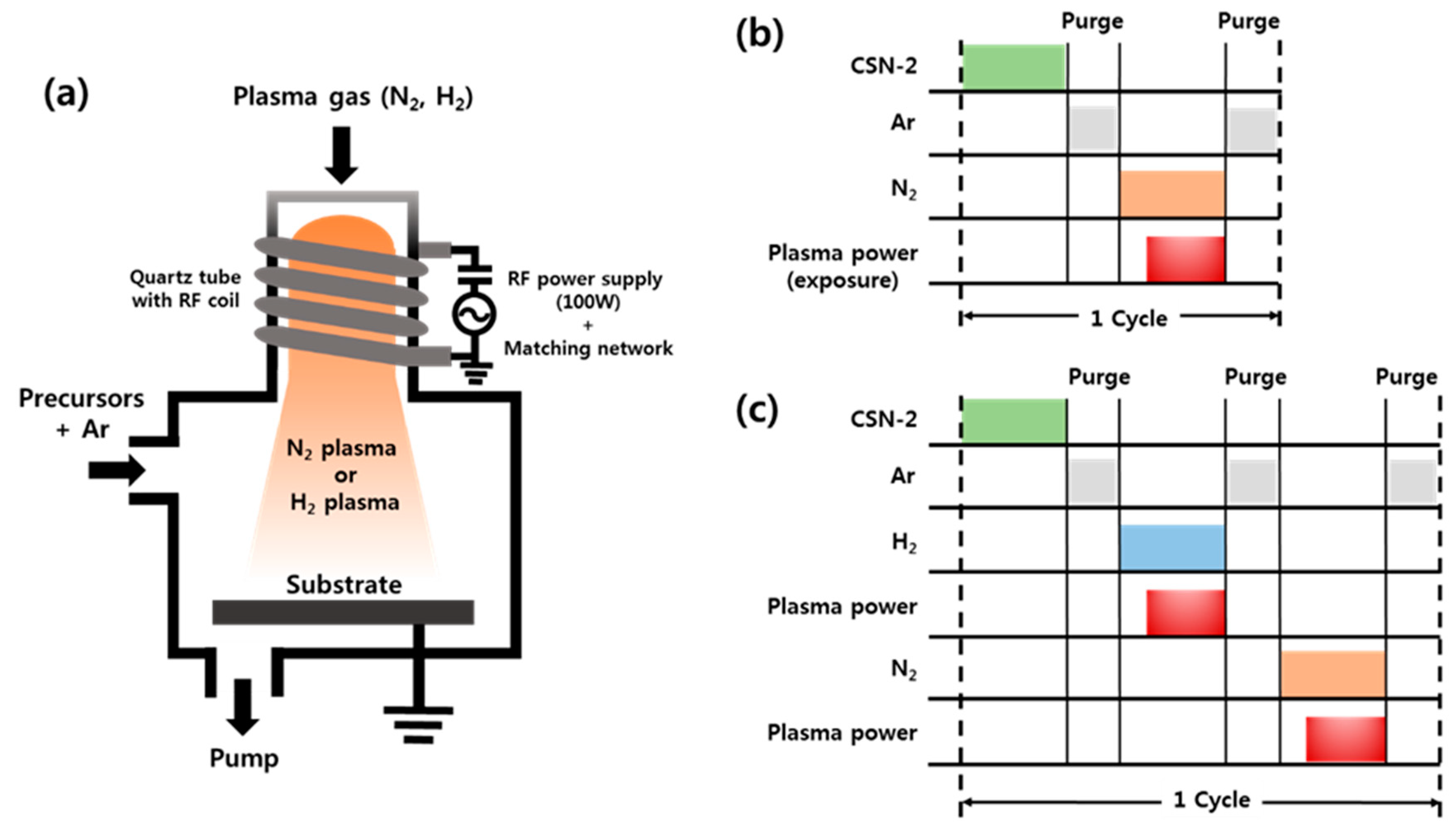
2. Materials and Methods

The Si wafer was a two-inch P-type Si (100) substrate for the deposition of SiNx, cleaned with diluted hydrofluoric acid for 2 min to remove native oxides. After cleaning, the substrate was loaded in the RPALD chamber. At first, SiNx films were deposited by RPALD with CSN-2 as the precursor and N2 plasma as the reactant (two-step). Precursors were heated at 60 °C using a heating jacket to obtain sufficient vapor pressure and Ar (50 sccm) was used as the carrier gas in the line during the precursor dosing and purging step. The delivery lines were heated to 70 °C to prevent precursor condensation. N2 plasma was generated by inductively coupled plasma (ICP) generated at a radio frequency of 13.56 MHz (Figure 1a). Deposition temperature was set in a wide range from 100 °C to 600 °C and the plasma power was fixed at 100 W. The recipe was selected as a standard which is composed of five stages (Figure 1b): CSN-2 dose time (3 s), precursor purge time (30 s), N2 reactant gas injection time (4 s), N2 plasma exposure time (20 s), and purge time (30 s). As shown in Figure 1c, we have developed the three-step process mentioned above, which adds H2 gas injection (4 s) and an H2 plasma exposure step (10, 20, and 30 s time variables) between the precursor purge and N2 gas injection step. In the previous ALD cycle, the precursor delivery lines were purged with 700 sccm of Ar to remove byproducts and residual gas. A base pressure in the reactor chamber of ~10-6 torr was obtained using a turbo-molecular pump.
The thickness and refractive index of the deposited SiNx films were measured by spectroscopic ellipsometry (SE) using a Nano-View SE MG-1000 operated at an incident angle of 70° (1.5–5.0 eV). To investigate the surface morphology of SiNx thin films, atomic force microscope (AFM; Park Systems, XE-7) was used. The chemical compositions of the SiNx films were investigated with auger electron spectroscopy (AES). The chemical bonding state was determined by X-ray photoelectron spectroscopy (XPS) using a PHI 700Xi with Mg Kα X-ray source (E = 1.254 keV). Film wet etch rates were evaluated in a diluted HF solution (H2O / HF = 100:1). Film thickness and step coverage were examined by transmission electron microscopy (TEM).

3. Results and Discussion
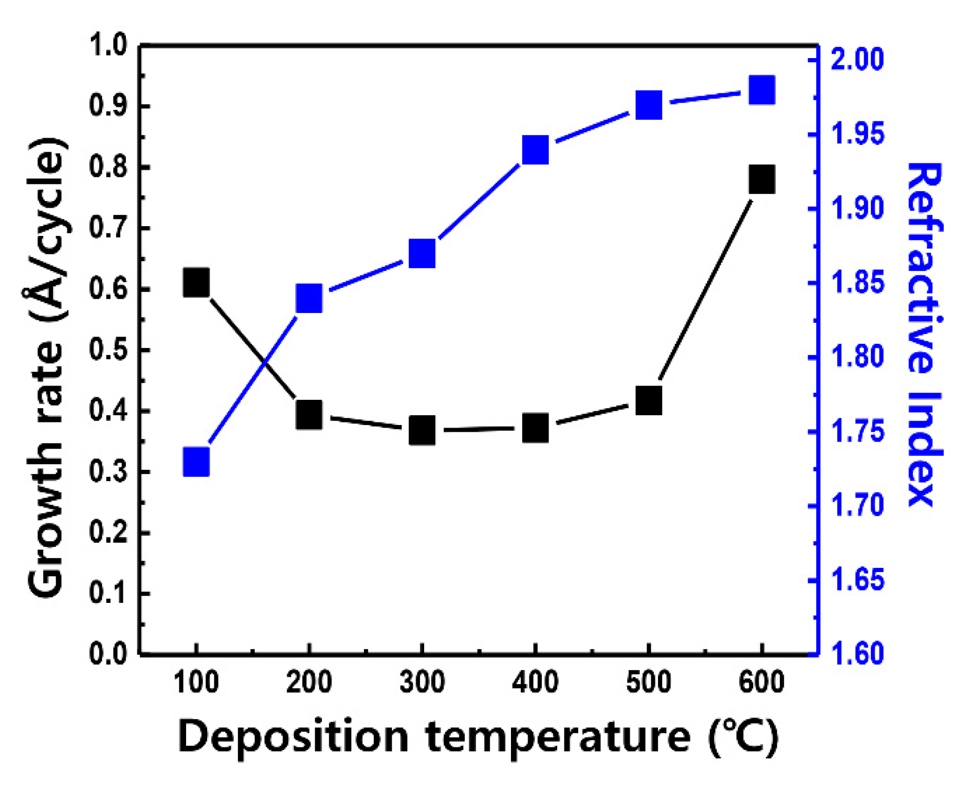
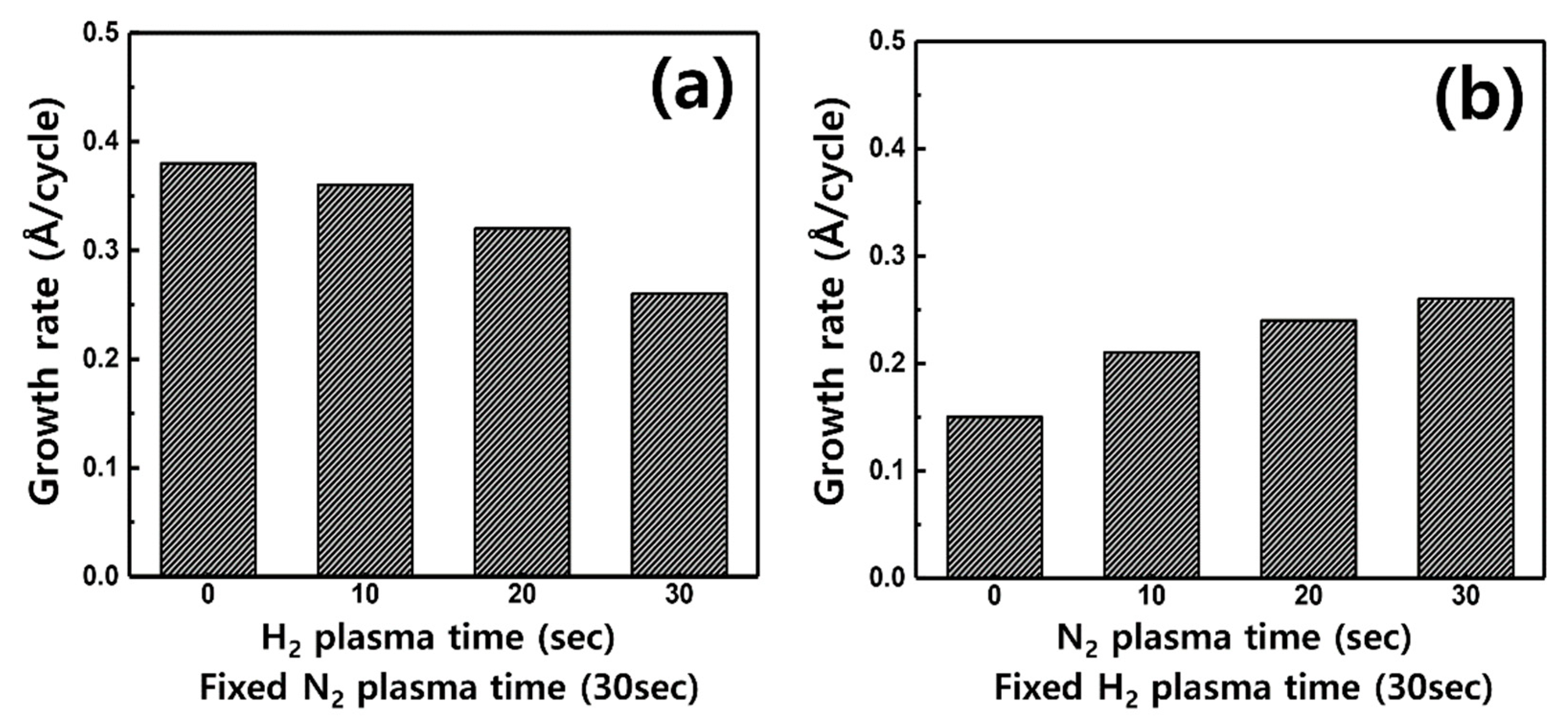
3.1. Process Window

The deposition rate of SiNx thin films was investigated as a function of precursor dosing time and plasma exposure time at 400 °C. The growth rate per cycle (GPC) increased and saturated at 0.38 Å/cycle, as CSN-2 dosing time increased to 5 s. An apparent saturation for GPC can also be investigated when the plasma exposure time was 20 s or longer. This GPC saturation indicates that the SiNx thin film RPALD process using CSN-2 and N2 plasma is a self-limited reaction with no thermal decomposition of the precursor.
We investigated the growth rate of SiNx thin films at various temperatures (100–600 °C) as shown in Figure 2. The growth rate of the SiNx thin film was nearly constant at 0.38 Å/cycle in the deposition temperature range of 200–500 °C, known as the ALD process window. In the temperature regions below 200 °C and above 500 °C, the self-limited reaction is disturbed depending on process temperature. The former is due to precursor condensation on the substrate and the latter is due to thermal decomposition of the precursor; a “CVD-like” process [25,26,27]. As the deposition temperature increased, the refractive index of SiNx increased to 1.98 which is similar to 2.01 of the stoichiometric SiNx thin film, indicating that the quality of the film was improved. It can be also assumed that the film density is improved by increasing the refractive index [28].

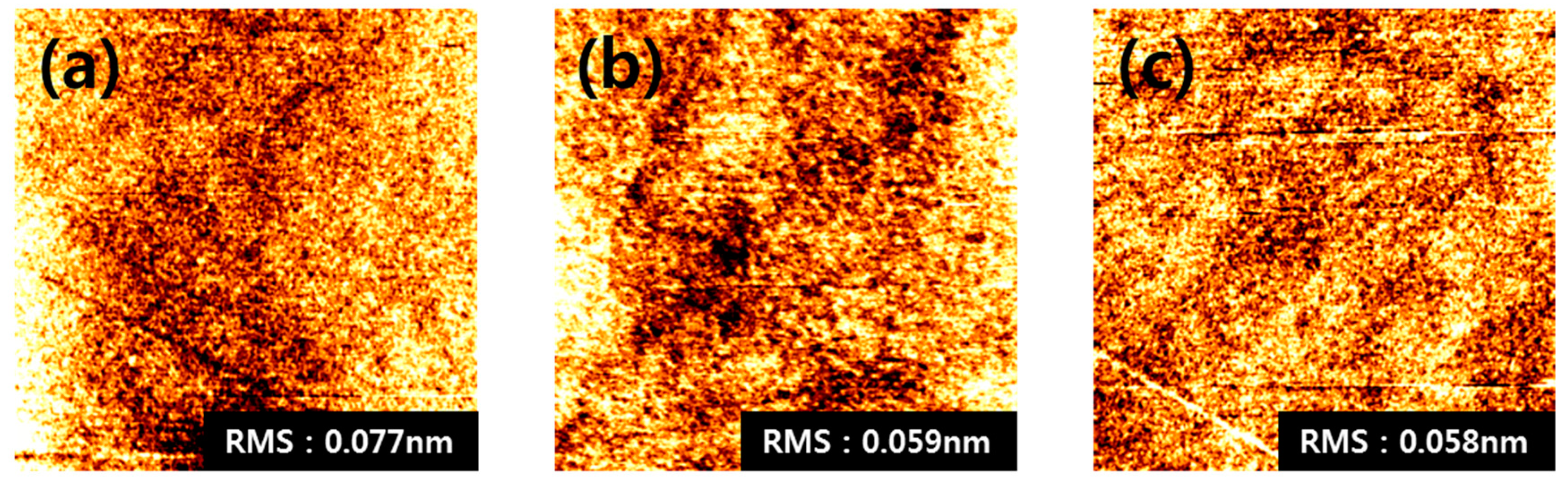
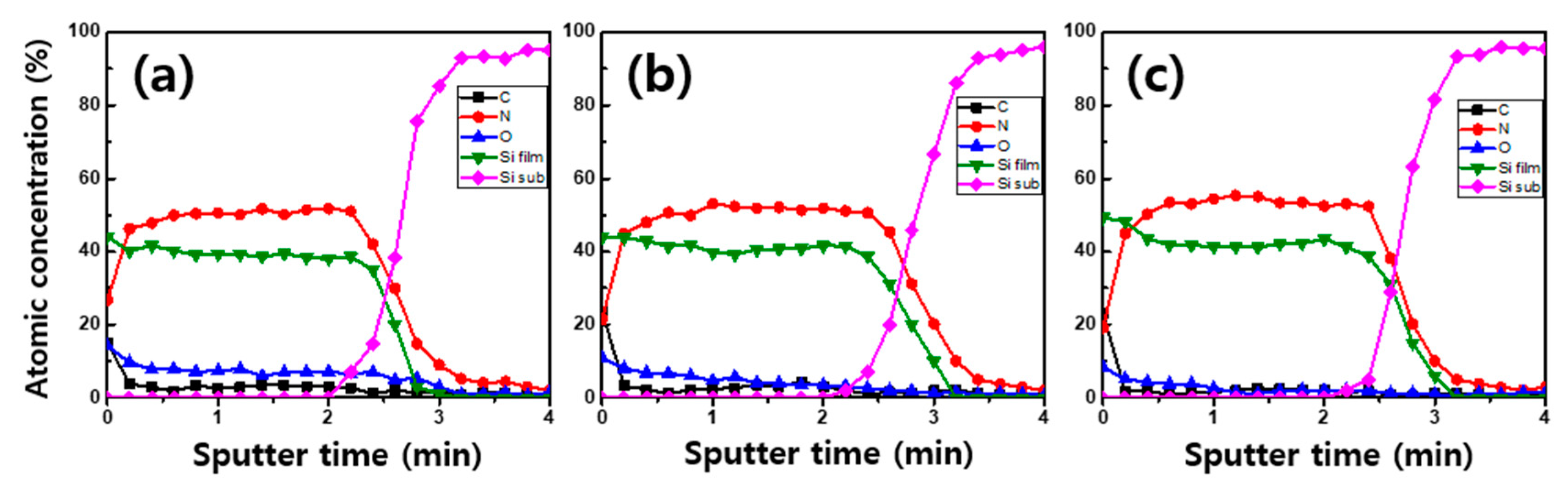
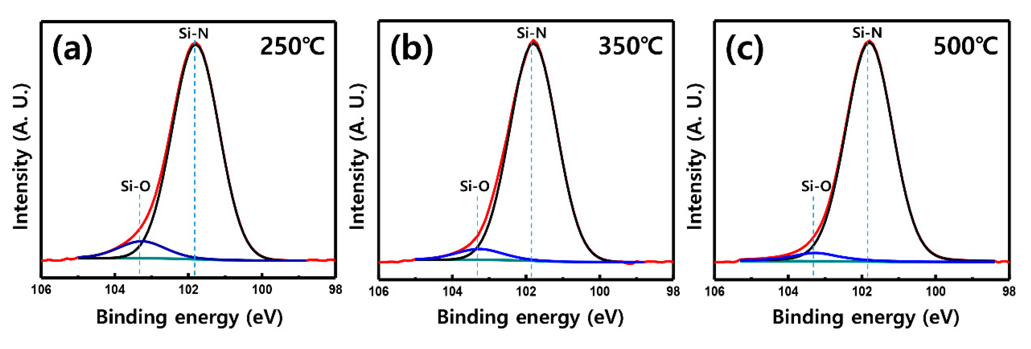
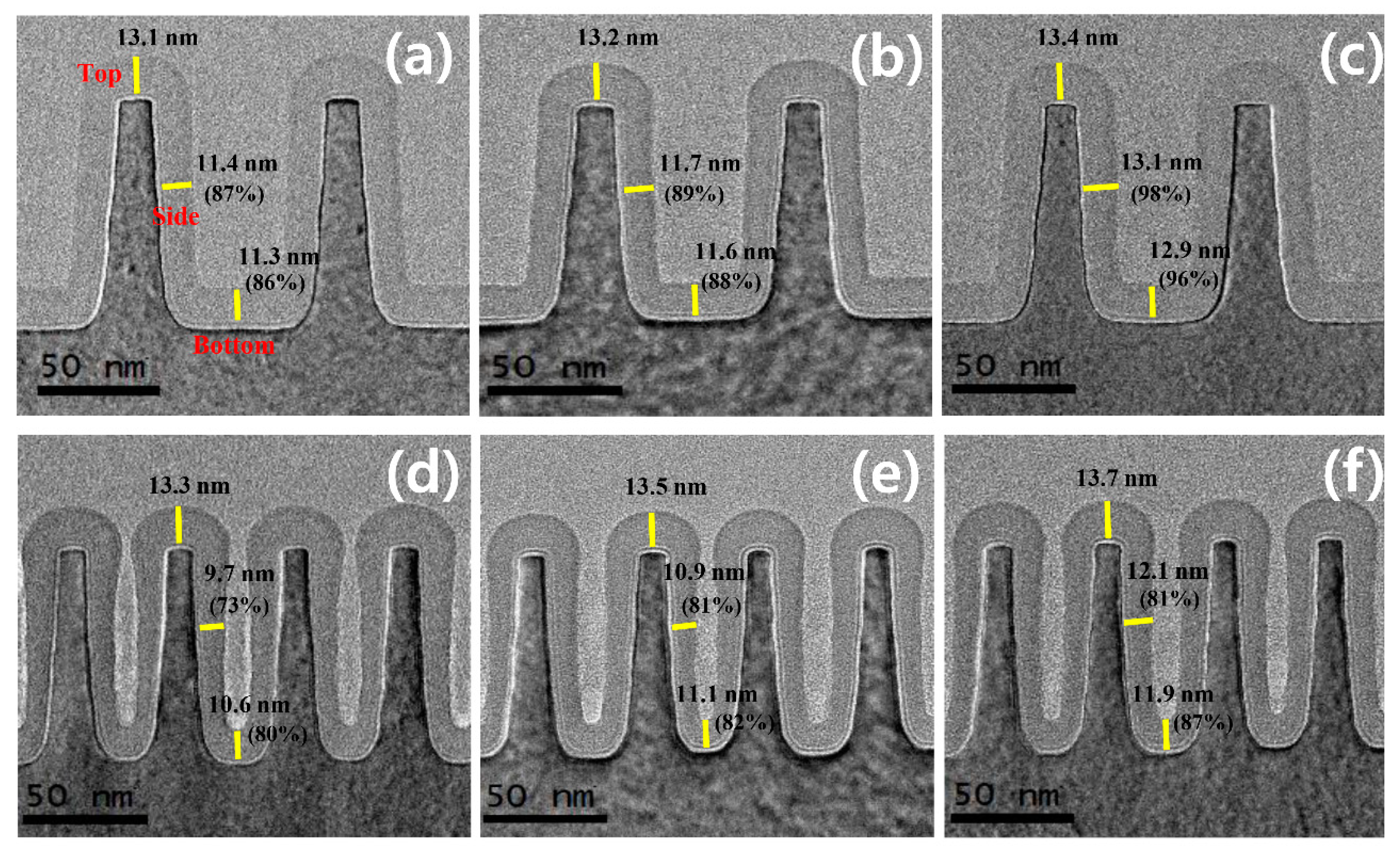
3.2. Characteristics of SiNx Thin Films

AFM was used to analyze the roughness of the SiNx thin film. Figure 3 shows AFM images of SiNx thin film deposited at 250 °C, 350 °C, and 500 °C, respectively. Figure 3a has an RMS (route mean square) value of 0.077 nm, if SiNx thin film was deposited at 500 °C, the value of the SiNx film is 0.058 nm. Compared with the SiNx thin film deposited at low temperature, the roughness was slightly decreased as the process temperature increased. However, the width of the increase is so small that all thin films seem to have high surface quality. Even though the thin film is processed by various temperature conditions, good uniformity in the film can be observed.
To investigate the chemical compositions of the SiNx thin films, depth profiles were measured by AES, as shown in Figure 4. According to the AES analysis, there was an absolute decrease in carbon content with deposition temperature, which means that sufficient thermal energy was contributed to the reaction. Also, the films deposited at low temperature were vulnerable to oxidation due to low film density. SiNx thin films deposited below 250 °C contain a considerable amount of oxygen, which was reduced with increasing deposition temperature to 500 °C and measured to be less than 2%. The constant N and Si atomic contents indicate a uniform film stoichiometry throughout the entire film thickness. The ratio of N to Si was 1.34, which is nearly a stoichiometric Si3N4 film.
The chemical binding states in each film were investigated using XPS analysis. With the XPS scans of Si 2p and N 1s peaks, we obtained information regarding the bonding behavior of SiNx, as shown in Figure 5 (N 1s peak not shown). The XPS spectrum corresponding to the Si 2p with peak at 101.82 eV is the signature of the Si–N bond. The spectra corresponding to the N 1s content with peaks centered at 397.72 eV are the signature of the N–Si bond. The Si 2p spectra showed that all the samples had peaks at 101.82 eV. In the N 1s spectra, all the samples exhibited a peak at 397.72 eV [16]. In other words, the deposited samples were nearly stoichiometric Si3N4 and no difference in binding energy state was shown when the deposition temperature increased from 250 to 500 °C. As shown in Figure 5, the Si 2p peak deconvolution was performed with the Si–N binding energy corresponding to 101.82 eV and the Si–O binding energy corresponding to 103.27 eV. References to XPS and AES data confirmed that the oxygen content decreased sharply as the deposition temperature increased [16].
The step coverage of SiNx thin film was investigated using trench-patterned wafers, as shown in Figure 6. The aspect ratio of the trench patterned wafer is 2.7 with a top trench width of 31.2 nm in a narrow pattern. SiNx thin film thickness was measured at the top, side, and bottom of the trench with film conformality. The step coverage of the films improved with increasing deposition temperature. In the narrow pattern, the temperature condition of 250 °C yielded side and bottom coverages of 73% and 80%. As the deposition temperature increased to 500 °C, improved film conformality was obtained with side and bottom coverages of 81% and 87%.
The wet etch rate (WER) test was performed to investigate SiNx etching properties. A diluted HF solution (1:100) was used. The LPCVD of Si3N4 film at 730 °C was referenced for the WER test. As shown in Table 1, the wet etch rate decreased with increasing deposition temperature. In the above-mentioned Figure 2, as the deposition temperature increases, the film density also improved due to the increase of the refractive index [28,29]. It is understandable that the wet etch rate decreases with increasing deposition temperature, considering the fact that the film density is inversely proportional to WER [17].
The physical properties of the SiNx film based on the CSN-2 precursor have been studied. Thin films with good step coverage and excellent etching properties were obtained at 500 °C. In order to improve the progress made through the previously described two-step process (CSN-2/purge/N2 plasma/purge), an H2 plasma step was added between the CSN-2 and N2 plasma step to improve the characteristics of the thin film used as a gate spacer. In logic devices, the actual gate spacer process proceeds at temperatures below 400 °C to prevent implant out-diffusion and unwanted metal oxidation in the high-k metal gate (HKMG). Thus, we performed a comparative study between the two-step and three-step processes at 350 °C.
N2 plasma not only removes the ligand of the precursor, but also facilitates the chemisorption of the silicon precursor. However, the N radicals have an exceptionally short life time compared to H radicals or O radicals. Due to this short lifetime, recombination loss occurs and the ligand is not completely removed from the precursor, such that the step coverage and quality of the thin film deteriorates. By introducing the H2 plasma before the N2 plasma, efficient ligand removal from the surface can be achieved by H radicals with a long lifetime. The SiNx films with an excellent step coverage and wet etch rate were obtained [21,22,23,24].
As shown in Figure 7a, as the H2 plasma exposure time increases in the three-step process, the deposition rate decreases because the influence of the H2 plasma forms an NH2 or SiH group, which make reactions with the precursor difficult. In contrast, the deposition rate improved by fixing the H2 plasma and increasing the N2 plasma time as seen in Figure 7b. This is because the N2 plasma regenerates the reaction sites on the surface where the -H or -NH2 group is terminal and forms an undercoordinated surface. Therefore, the precursor easily reacts with the surface [16].
As shown in Figure 8, TEM images show step coverage with various H2 plasma exposure times. Compared with the case of As-dep films, the step coverage improves with increasing H2 plasma exposure time. In general, we can observe that the step coverage is greatly improved at the bottom/top compared to the side/top. In the narrow pattern, the side step coverage increased from 82% to 105% and the bottom step coverage increased from 90% to 110%. The narrow pattern is shown in Figure 8d–f. When the H2 plasma exposure time is 20 s, conformality was as good as the thin film proceeded at 500 °C. In Table 2, the WER was investigated at the same condition. As observed, the longer the H2 plasma exposure time, the lower the etch rate, which decreased from 43 to 32 Å/min.
It was confirmed that the step coverage and wet etching characteristics were improved with H2 plasma time by applying the low temperature process, which is necessary for the deposition of the gate spacer. Through process improvement, we were able to concentrate on the physical properties of the SiNx thin film. It was found that a high quality thin film could be obtained for the gate spacer depending on how the unique characteristics of the plasma reactant are utilized in the ALD process.

4. Conclusions

In this work, physical and chemical properties of SiNx as a gate spacer were evaluated. The process environment was implemented in a remote plasma ALD system designed to overcome the limitations of the high thermal budget of thermal ALD and to minimize the thin film damage that can occur in direct plasma ALD [19]. The atomic concentration and chemical binding state were confirmed by deposition of SiNx with CSN-2 and N2 plasma. The fundamental properties of step coverage and wet etch rate were analyzed. The H2 plasma step was introduced before the N2 plasma step, which is a three-step process resulting in a reduction of growth rate. Many studies using NH3 plasma as a reactant have been performed. In our research, the H2 plasma and N2 plasma were used as reactants, respectively, instead of NH3 plasma. We compared the effect of the two-step process (only N2 plasma) with the three-step process at low temperature (≤400 °C) [22]. According to the results of the study for the narrow pattern, the longer H2 plasma exposure time increased the side step coverage from 81% to 105%, and bottom step coverage increased from 90% to 110%. In addition, the wet etch rate was reduced from 43.2 to 32.4 Å/min. Based on the results of this study, it was confirmed that the step coverage and the wet etching characteristics of the gate spacer thin film can be appropriately controlled by the optimization process.

Author Contributions

Data curation, H.C. (Hyeongsu Choi), H.P., C.J., S.S., H.Y., Y.K., J.-W.K., K.K., Y.C., and S.P.; Original draft preparation, H.C. (Haewon Cho); writing—review and editing, N.L.; Supervision, H.J.

Funding

This work was supported by the Nano Material Technology Development Program (2014M3A7B4049367) through the National Research Foundation (NRF) of Korea funded by the Ministry of Science and ICT (MSIT), Korea. This work is supported by the Samsung Electronics’ University R&D program [Study of high step coverage ONO thin film for CTF device].

Conflicts of Interest

The authors declare no conflict of interest.

References

  1. Park, J.-M.; Jang, S.J.; Yusup, L.L.; Lee, W.-J.; Lee, S.-I. Plasma-enhanced atomic layer deposition of silicon nitride using a novel silylamine precursor. ACS Appl. Mater. Interfaces 2016, 8, 20865–20871. [Google Scholar] [CrossRef] [PubMed]
  2. Weeks, S.; Nowling, G.; Fuchigami, N.; Bowes, M.; Littau, K. Plasma enhanced atomic layer deposition of silicon nitride using neopentasilane. J. Vac. Sci. Technol. A 2016, 34, 01A140. [Google Scholar] [CrossRef]
  3. Andringa, A.-M.; Perrotta, A.; Peuter, K.; Knoops, H.C.M.; Kessles, W.M.M.; Creatore, M. Low-temperature plasma-assisted atomic layer deposition of silicon nitride moisture permeation barrier layers. ACS Appl. Mater. Interfaces 2015, 7, 22525–22532. [Google Scholar] [CrossRef] [PubMed]
  4. Faraz, T.; Drunen, M.; Knoops, H.C.M.; Mallikarjunan, A.; Buchanan, I.; Hausmann, D.M.; Henri, J.; Kessels, W.M.M. Atomic layer deposition of wet-etch resistant silicon nitride using Di(sec-butylamino) silane and N2 plasma on planar and 3D substrate topographies. ACS Appl. Mater. Interfaces 2017, 9, 1858–1869. [Google Scholar] [CrossRef] [PubMed]
  5. Koehler, F.; Triyoso, D.H.; Hussain, I.; Antonioli, B.; Hempel, K. Challenges in spacer process development for leading-edge high-k metal gate technology. Phys. Status Solidi C 2014, 11, 73–76. [Google Scholar] [CrossRef]
  6. Belyansky, M.; Conti, R.; Khan, S.; Zhou, X.; Klymko, N.; Yao, Y.; Madan, A.; Tai, L.; Flaitz, P.; Ando, T. Atomic layer deposition of sidewall spacers: Process, equipment and integration challenges in state-of-art technologies. ECS. Trans. 2014, 61, 39–45. [Google Scholar] [CrossRef]
  7. Treichel, M. Low dielectric constant materials. J. Electron. Mater. 2001, 30, 290–298. [Google Scholar] [CrossRef]
  8. Jang, W.; Jeon, H.; Song, H.; Kim., H.; Park, J.; Kim, H.; Jeon, H. The effect of plasma power on the properties of low-temperature silicon nitride deposited by PRALD for a gate spacer. Phys. Status Solidi A-Appl. Mat. 2015, 212, 2785–2790. [Google Scholar] [CrossRef]
  9. Jang, W.; Kim, H.; Kweon, Y.; Jung, C.; Cho, H.; Shin, S.; Kim, H.; Lim, K.; Jeon, H.; Lim, H. Remote plsma atomic layer deposition of silicon nitride with bis(dimethylaminomethyl-silyl)trimethylsilyl amine and N2 plasma for gate spacer. J. Vac. Sci. Technol. A 2018, 36, 031514. [Google Scholar] [CrossRef]
  10. Meng, X.; Byun, Y.-C.; Kim, H.S.; Lee, J.S.; Lucero, A.T.; Cheng, L.; Kim, J. Atomic layer deposition of silicon nitride thin films: A review of recent progress, challenges, and outlooks. Materials 2016, 9, 1007. [Google Scholar] [CrossRef]
  11. Kariniemi, M.; Niinisto, J.; Vehkamaki, M.; Kemell, M.; Ritala, M.; Leskela, M. Conformality of remote plasma-enhanced atomic layer deposition processes: An experimental study. J. Vac. Sci. Technol. A 2012, 30, 01A115. [Google Scholar] [CrossRef]
  12. George, S.M. Atomic layer deposition: An overview. Chem. Rev. 2010, 110, 111–131. [Google Scholar] [CrossRef] [PubMed]
  13. Profijt, H.B.; Potts, S.E.; van de Sanden, M.C.M.; Kessels, W.M.M. Plasma-Assisted atomic layer deposition: Basics, opportunities, and challenges. J. Vac. Sci. Technol. A 2011, 29, 050801. [Google Scholar] [CrossRef]
  14. Crowell, J.E. Chemical methods of thin films deposition: Chemical vapor deposition, atomic layer deposition, and related technologies. J. Vac. Sci. Technol. A 2003, 21, S88–S95. [Google Scholar] [CrossRef]
  15. King, S.W. Plasma enhanced atomic layer deposition of SiNx:H and SiO2. J. Vac. Sci. Technol. A 2011, 29, 041501. [Google Scholar] [CrossRef]
  16. Jang, W.; Jeon, H.; Kang, C.; Song, H.; Park, J.; Kim, H.; Seo, H.; Leskela, M.; Jeon, H. Temperature dependence of silicon nitride deposited by remote plasma atomic layer deposition. Phys. Status Solidi Appl. and Mater. 2014, 211, 2166–2171. [Google Scholar] [CrossRef]
  17. Provine, J.; Schindler, P.; Kim, Y.; Walch, S.P.; Kim, H.J.; Kim, K.-H.; Prinz, F.B. Correlation of film density and wet etch rate in hydrofluoric acid of plasma enhanced atomic layer deposited silicon nitride. AIP Adv. 2016, 6, 065012. [Google Scholar] [CrossRef] [Green Version]
  18. Profijit, H.B.; Kessels, W.M.M. Ion bombardment during plasma-assisted atomic layer deposition. ECS Trans. 2012, 50, 23–34. [Google Scholar] [CrossRef]
  19. Van Hemmen, J.L.; Heil, S.S.S.; Klootwijk, J.H.; Roozeboom, F.; Hodson, C.J.; van de Sanden, M.C.M.; Kessels, W.M.M. Plasma and thermal ALD of Al2O3 in a commercial 200mm ALD reactor. J. Electrochem. Soc. 2007, 154, G165–G169. [Google Scholar] [CrossRef]
  20. Kim, H.W.; Song, H.S.; Shin, C.H.; Kim, K.S.; Jang, W.C.; Kim, H.J.; Shin, S.Y.; Jeon, H.T. Dielectric barrier characteristics of Si-rich silicon nitride films deposited by plasma enhanced atomic layer deposition. J. Vac. Sci. Technol. A 2017, 35, 01A101. [Google Scholar] [CrossRef]
  21. Park, J.-M.; Jang, S.J.; Lee, S.I.; Lee, W.J. Novel cyclosilazane-type silicon precursor and two-step plasma for plasma-enhanced atomic layer deposition of silicon nitride. ACS Appl. Mater. Interfaces 2018, 10, 9155–9163. [Google Scholar] [CrossRef] [PubMed]
  22. Ovanesyan, R.A.; Hausmann, D.M.; Agarwal, S. A three-step atomic layer deposition process for SiNx using Si2Cl6, CH3NH2, and N2 plasma. ACS Appl. Mater. Interfaces 2018, 10, 19153–19161. [Google Scholar] [CrossRef] [PubMed]
  23. Ande, C.K.; Knoops, H.C.M.; Peuter, K.D.; Drunen, M.V.; Elliott, S.D.; Kessels, W.M.M. Role of surface termination in atomic layer deposition of silicon nitride. J. Phys. Chem. Lett. 2015, 6, 3610–3614. [Google Scholar] [CrossRef] [PubMed]
  24. Yusup, L.L.; Park, J.M.; Noh, Y.-H.; Kim, S.-J.; Lee, W.-J.; Park, S.; Kwon, Y.-K. Reactivity of different surface sites with silicon chlorides during atomic layer deposition of silicon nitride. RSC Adv. 2016, 6, 68515–69524. [Google Scholar] [CrossRef]
  25. Kim, H. Atomic layer deposition of metal and nitride thin films: Current research efforts and applications for semiconductor device processing. J. Vac. Sci. Technol. B 2013, 21, 2231–2261. [Google Scholar] [CrossRef]
  26. Kim, H. Characteristics and applications of plasma enhanced-atomic layer deposition. Thin Solid Films 2011, 519, 6639–6644. [Google Scholar] [CrossRef]
  27. Puurunen, R.L. Surface chemistry of atomic layer deposition: A case study for the trimethylaluminum/water process. J. Appl. Phys. 2005, 97, 121301. [Google Scholar] [CrossRef]
  28. Mergel, D.; Buschendorf, D.; Eggert, S.; Grammes, R.; Samset, B. Density and refractive index of TiO2 films prepared by reactive evaporation. Thin Solid Films 2000, 371, 218–224. [Google Scholar] [CrossRef]
  29. Panja, R.; Roy, S.; Jana, D.; Maikap, S. Impact of device size and thickness of Al2O3 film on the Cu pillar and resistive switching characteristics for 3D cross-point memory application. Nanoscale. Res. Lett 2014, 9, 692–702. [Google Scholar] [CrossRef]
Figure 1. Schematic images of the (a) remote plasma atomic layer deposition (RPALD) system and process sequence (b) without H2 plasma and (c) with H2 plasma.
Applsci 09 03531 g001
Figure 2. Effect of growth rate and refractive index as a function of deposition temperature at a plasma power of 100 W.
Applsci 09 03531 g002
Figure 3. Atomic force microscopy (AFM) images (5 × 5 μm) of RPALD SiNx film deposited at (a) 250 °C, (b) 350 °C, and (c) 500 °C.
Applsci 09 03531 g003
Figure 4. Auger electron spectroscopy (AES) depth profiles of RPALD SiNx film deposited at (a) 250 °C, (b) 350 °C, and (c) 500 °C.
Applsci 09 03531 g004
Figure 5. Si 2p peak deconvolution of X-ray photoelectron spectroscopy (XPS) spectra for RPALD SiNx film deposited at (a) 250 °C, (b) 350 °C, and (c) 500 °C.
Applsci 09 03531 g005
Figure 6. Transmission electron microscopy (TEM) images for step coverage of the RPALD SiNx film as a function of deposition temperature in a wide pattern at (a) 250 °C, (b) 350 °C, and (c) 500 °C and in a narrow pattern at (d) 250 °C, (e) 350 °C, and (f) 500 °C.
Applsci 09 03531 g006
Figure 7. (a) The growth rate as a function of H2 plasma exposure time (N2 plasma exposure time fixed at 30 s); (b) The growth rate as a function of N2 plasma exposure time (H2 plasma exposure time fixed at 30 s).
Applsci 09 03531 g007
Figure 8. Cross sectional TEM images for step coverage of the RPALD SiNx film as a function of H2 plasma exposure time in a wide pattern for (a) 10 s, (b) 20 s, and (c) 30 sec and in a narrow pattern for (d) 10 s, (e) 20 s, and (f) 30 s. All the samples were deposited at 350 °C.
Applsci 09 03531 g008
Table 1. Wet etch rate of the RPALD SiNx film as a function of deposition temperature.
Temp. (°C)250350500
Wet Etch Rate (Å/min)574335
Table 2. Wet etch rate as a function of H2 plasma exposure time in the three-step process.
H2 Plasma Time (s)0102030
WER (Å/min)43393432

