Article

A Mid-Infrared Narrowband Absorber Based on a Subwavelength Fine-Structured Silicon–Gold Metagrating

1
Department of Physics, National University of Defense Technology, Changsha 410073, China
2
College of Aerospace Science and Engineering, National University of Defense Technology, Changsha 410073, China
*
Author to whom correspondence should be addressed.
Appl. Sci. 2019, 9(23), 5022; https://doi.org/10.3390/app9235022
Submission received: 16 October 2019 / Revised: 15 November 2019 / Accepted: 18 November 2019 / Published: 21 November 2019
(This article belongs to the Special Issue Mid-Infrared and THz Spectroscopy: Innovative Tools and Applications)

Abstract

:
A subwavelength fine-structured silicon–gold metagrating was designed for realizing mid-infrared (mid-IR) narrowband absorbers. The metagrating consisted of a silicon grating on the stack of a gold film and a quartz substrate. The silicon grating consisted of two periodically arranged silicon strips in each unit cell. The numerical results reveal that perfect absorption of the traverse-magnetic (TM) polarized light at a wavelength of 4.071 μm can be achieved, with an absorption rate of ~99.2% and an absorption full-width at half-maximum (FWHM) bandwidth of ~31 nm. Thus, the proposed structure is useful for the spectral control of mid-IR signals. When used as a refractive index sensor, the structure has a measuring range of 1.0–2.0 with a quasi linear response, with a figure of merit (FOM) of ~103.

1. Introduction

Recently, perfect absorbers (PAs) have attracted great attention because they have a variety of potential applications. PAs with a broad operating bandwidth are useful in photonic detection [1] and light energy acquisition [2], whereas PAs with a narrow operating bandwidth are advantageous for sensing [3], filtering [4], and selective thermal emitting [5]. In particular, narrowband PA-based refractive index sensors are very promising due to their simple structure and high-throughput detection [6]. Researchers have presented this type of sensor which exhibits good performance [7,8]. Furthermore, thermo-optical sensing can also be achieved by narrowband PAs operating in the terahertz spectral region [9].
To achieve narrowband PAs, many researchers have investigated the use of all-metal structures or tri-/multi-layer metal-insulator-metal (MIM) structures [10,11,12,13,14]. However, fabrication of these structures is costly due to their incompatibility with complementary metal oxide semiconductor (CMOS) fabrication processes [15]. For this reason, there has been an increasing interest in realizing narrowband PAs by dielectric structure on metal systems [16,17,18]. In comparison with metallic PAs, this type of absorber can save the fabrication cost [19]. Such absorbers typically have one or more dielectric waveguide layer between the grating and the metallic substrate. They can generate ultra-narrow absorption peaks, but their structures are relatively complex. To simplify the structure, a dielectric grating can be placed on top of a metallic substrate/film directly [20,21,22,23,24,25,26]. For example, in 2004, Fitio et al. theoretically studied the resonance absorption of a usual dielectric grating on a metal system [25]. In 2017, Liao et al. numerically presented a narrowband PA constructed by a usual and a compound dielectric grating on a metallic substrate [26,27]. These absorbers can also provide ultra-narrow absorption bandwidths.
Most of the structures above used low-index dielectric gratings, thus showing obvious disadvantages. For example, the grating grooves could have large depth–width ratios (>10) and were difficult to fabricate. The designed peaks could disappear in high-index surroundings, which limited their practical applications in refractive index sensing. Moreover, they mainly operated in the visible and near-infrared spectral region.
However, such narrowband PAs operating in the mid-infrared (mid-IR) spectral region are particularly useful, as in the mid-IR spectral region there are various molecular fingerprint spectra [28]. When used with diode lasers and quantum cascade lasers, these narrowband PAs can be very promising in a number of applications, including spectroscopic sensing and gas detection [29,30].
In this work, we proposed a mid-IR narrowband PA for sensing applications. The PA was achieved by placing a fine-structured silicon grating on a gold film. The silicon grating consisted of two narrow silicon strips in each unit cell, which enabled the excited resonance mode to be low-loss. Thus, the absorber provided a narrow absorption peak at a wavelength of 4.071 μm with a high absorption rate. The absorber is useful for the spectral control of mid-IR signals. When used as a refractive index sensor, it has the advantage of still being effective in high-index surroundings. The proposed absorber is very simple and is fully compatible with current CMOS fabrication processes.

2. Structure Design and Principle

Figure 1a shows aschematic view of the designed narrowband PA. The structure consisted of a silicon grating on a stack of a gold film and a quartz substrate. The period of the structure is Λ 1 . The incident beam was a traverse-magnetic (TM) polarized plane wave, whose polarization was perpendicular to the silicon strips. Figure 1b shows a single unit cell of the PA. In each unit cell, there were two periodically arranged silicon strips, with a period of Λ 2 and a filling-factor of f 2 . Thus, the silicon grating had an overall-period of Λ 1 and a sub-period of Λ 2 . The width of each silicon strip was f 2 Λ 2 . The thickness of the gold film was h 1 . The height of the silicon grating was h 2 .
The silicon grating could diffract the incident light into different orders. The in-plane wavevectors of various diffraction-orders were determined by [31]
k ( i ) = k sin α + 2 π i Λ 1
where k is the wavevector of the incident light, α is the incident angle, k ( i ) is the in-plane wavevector of the i th diffraction-order, and i = 0, ±1, ±2, …, ±N. By choosing proper grating parameters, the (+1, −1) orders could be coupled with planar propagated plasmonic modes. Under this condition, the resonant coupling between the plasmonic mode and the lattice mode induced a strong modulation of the optical response. According to the wavevector matching condition, the coupling processes satisfied
2 π n eff ( + 1 ) λ ( + 1 ) = β ( + 1 ) = k sin α + 2 π Λ 1
2 π n eff ( 1 ) λ ( 1 ) = β ( 1 ) = k sin α 2 π Λ 1
where β and n eff are the in-plane wavevector and effective index of the planar plasmonic mode, λ ( + 1 ) and λ ( 1 ) stand for the resonance wavelengths. These resonances resulted in absorption peaks at λ ( + 1 ) and λ ( 1 ) . Under the normal incidence condition ( α = 0 ), there was only a single absorption peak because λ ( + 1 ) = λ ( 1 ) .
To investigate the resonance properties, finite-difference time-domain (FDTD) simulations were carried out. In the simulations, optical parameters of Au and Si in [32] were used.

3. Results and Physical Understanding

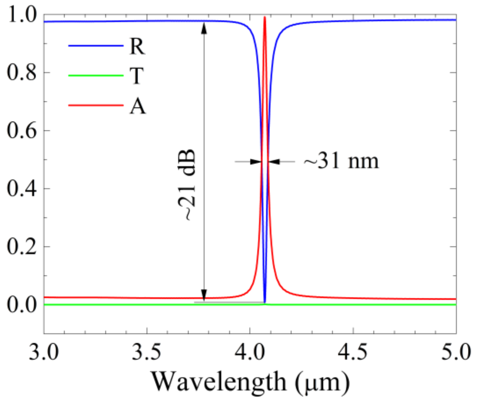
Figure 2 shows the simulated spectral responses of our structure at normal incidence. The structure parameters were chosen to be Λ 1 = 3.5 μm, h 1 = 0.1 μm, h 2 = 0.7 μm, Λ 2 = 0.7 μm, and f 2 = 0.37. Based on these parameters, we knew that the width of each silicon strip was f 2 Λ 2 = 259 nm. As can be observed in Figure 2, the transmission was nearly zero in the investigated spectral region. There was only a single reflection dip across the 3–5 μm wavelength range. The reflection dip was at a wavelength of 4.071 μm with an intensity extinction of ~21 dB. Thus, based on the proposed structure, a mid-IR narrowband notch filter operating in the reflection mode can be achieved. In comparison with notch filters presented in [4] and [19], our structure had the advantage of a narrower stop band. Compared with those in [17,26,27], our filter was simpler in structure.
The absorption spectrum A ( λ ) was calculated by 1 T ( λ ) R ( λ ) . The backscattered light was included in R ( λ ) . We obtained a single absorption peak at 4.071 μm, as shown in Figure 2. The peak had a high absorption rate on resonance (~99.2%). The full-width at half-maximum (FWHM) linewidth of the absorption peak was ~31 nm, corresponding to a Q-factor of ~137. These results indicate that our structure can realize perfect absorption of the TM-polarized light at a wavelength of 4.071 μm.
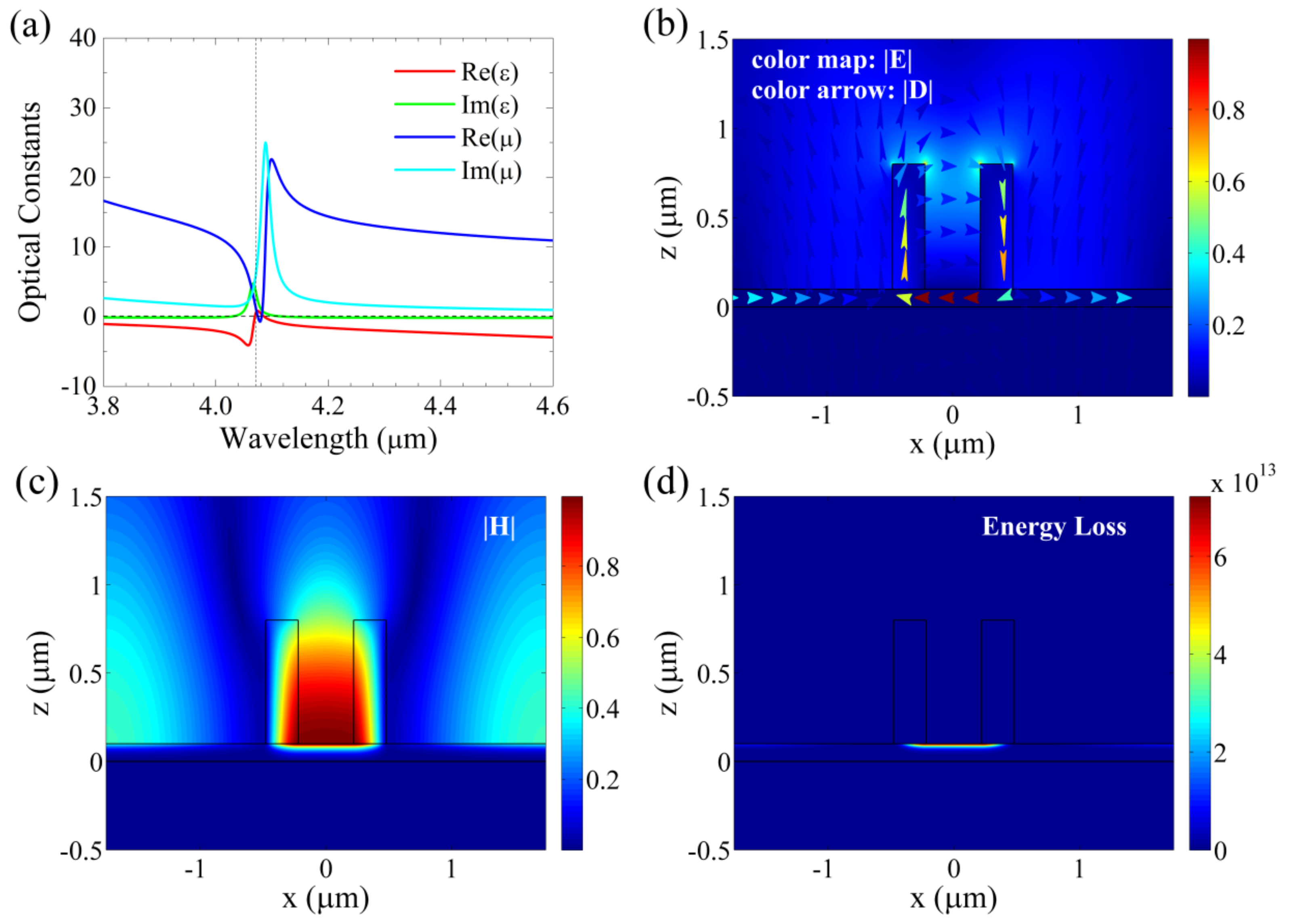
In order to understand the spectral responses illustrated in Figure 2, we retrieved the optical constants for the designed narrowband PA. Figure 3a plots the retrieved ε ( λ ) and μ ( λ ) , which were obtained by the inversion of the transmission and reflection coefficients ( S parameters) [33]. As is seen, either Re( ε ) or Re( μ ) was negative in the investigated wavelength range. This indicates that there was no transmission across the wavelength range. Moreover, at a wavelength of 4.071 μm (dashed line), both Re( ε ) and Re( μ ) crossed zero. This suggests that the reflection at a wavelength of 4.071 μm was minimized [34]. As a result, at a wavelength of 4.071 μm, the absorption was maximized.
To further understand the absorption mechanism, the electric field E and the displacement current D = ε E distributions are plotted in Figure 3b; the magnetic field H distribution is plotted in Figure 3c. In Figure 3b, we can observe that the electric field was concentrated strongly at the silicon ridges. The silicon slit was surrounded by a strong displacement current loop. For this reason, the magnetic field confined in the silicon slit was strong, as shown in Figure 3c. These results indicate that the electromagnetic resonance was excited in our structure. Figure 3d illustrates the simulated energy loss at 4.071 μm. It is observed that the energy dissipation was attributed to the Ohmic loss in the gold film. Energy loss mainly occurred in the gold film beneath the two silicon strips, because there the displacement current was strong.
In comparison with the usual dielectric-metal structures in the literature [19], our structure enabled the electromagnetic field on resonance to be away from the gold film. Therefore, the loss of the resonance mode decreased, and the FWHM of the absorption peak was narrowed. In addition, the electromagnetic field outside the silicon strips would be advantageous for refractive index sensing of the surrounding medium. In the following, we will show this.

4. Discussion

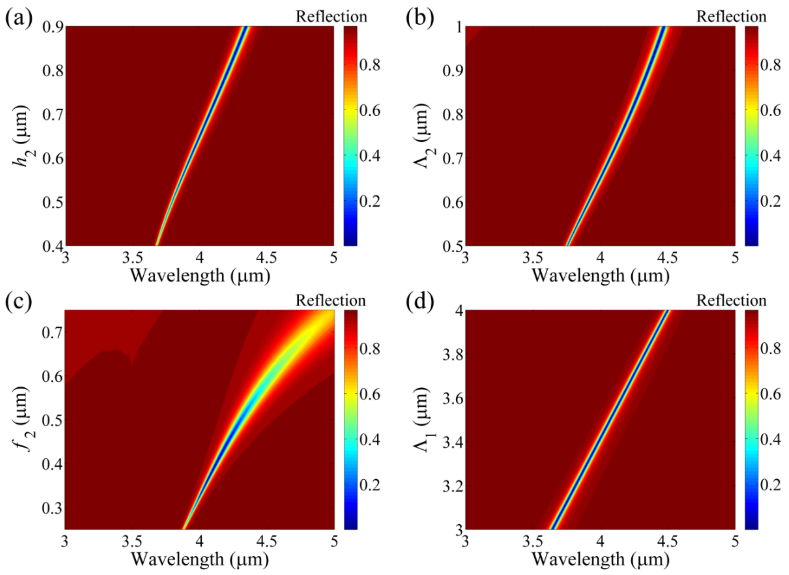
We first investigated the influences of the geometric parameters. Figure 4 shows the simulated reflection spectra when independently adjusting a certain parameter. As seen in Figure 4, the peak exhibited a redshift when the grating height h 2 , the sub-period Λ 2 , the sub-filling-factor f 2 , or the structure period Λ 1 increased. These can be explained based on Equations (2) and (3) as follows. As h 2 , Λ 2 , or f 2 increases, the silicon-to-gold ratio p = 2 f 2 Λ 2 h 2 / Λ 1 h 1 in each unit cell increases. Accordingly, the effective index of the plasmonic mode n eff increases, leading to a redshift of the resonance wavelength. Compared with those in Figure 4a,b, the more significant redshift in Figure 4c is due to the larger increase in n eff . However, the redshift in Figure 4d is mainly attributed to the increase in Λ 1 .
As seen in Figure 4a, a slight increase in the FWHM was observed when h 2 increased. This is mainly because the confined magnetic field in the silicon slit and the displacement current in the gold film increased. In Figure 4b, the FWHM also increased slightly with an increased Λ 2 , which mainly resulted from the increase in the silicon slit width (corresponding to the increase in the energy dissipation length). In Figure 4c, the FWHM increased with an increased f 2 , which is mainly due to the narrower silicon slit at a larger f 2 . Since the electric field concentrates at the silicon ridges, a narrower silicon slit results in a stronger electric field, thus enlarging the displacement current. Both the increases in displacement current and energy dissipation length can lead to the increase in the energy dissipation rate, thus broadening the FWHM. Compared with those in Figure 4a,b, the FWHM in Figure 4c changed more significantly. The main reason for this is that the electric field at the silicon ridges is sensitive to the distance between the two silicon strips. Therefore, the energy dissipation rate changes dramatically with a different f 2 . However, in Figure 4d, the FWHM exhibited almost no change with an increased Λ 1 . This is because Λ 2 was also adjusted to keep Λ 2 / Λ 1 unchanged.
The results suggest that it is convenient to tune the absorption wavelength and bandwidth by adjusting the structure parameters. However, careful attention should be paid to the sub-filling-factor, because the FWHM of the absorption peak is very sensitive to the distance between the two silicon strips.
Figure 5 shows the calculated reflection spectra at different angles of incidence, where the incidence was tilted in the xz-plane. In Figure 5a, it can be observed that the peak splits at oblique incidence. As the incident angle increases, the two split peaks gradually separate from each other. These phenomena are in accord with Equations (2) and (3). In Figure 5b, we see that there are two narrow peaks with good intensity extinctions (~10 dB) at an incident angle of 2.4 degrees. Furthermore, when the incident angle was 3.8 degrees, there was a narrow absorption peak at ~3.8 μm with high intensity extinction (~22 dB). These results indicate that dual-band absorption can be achieved by adjusting the incident angle. Furthermore, perfect absorption of the TM-polarized light at a different wavelength (~3.8 μm) can be realized at the light incidence angle of 3.8 degrees.
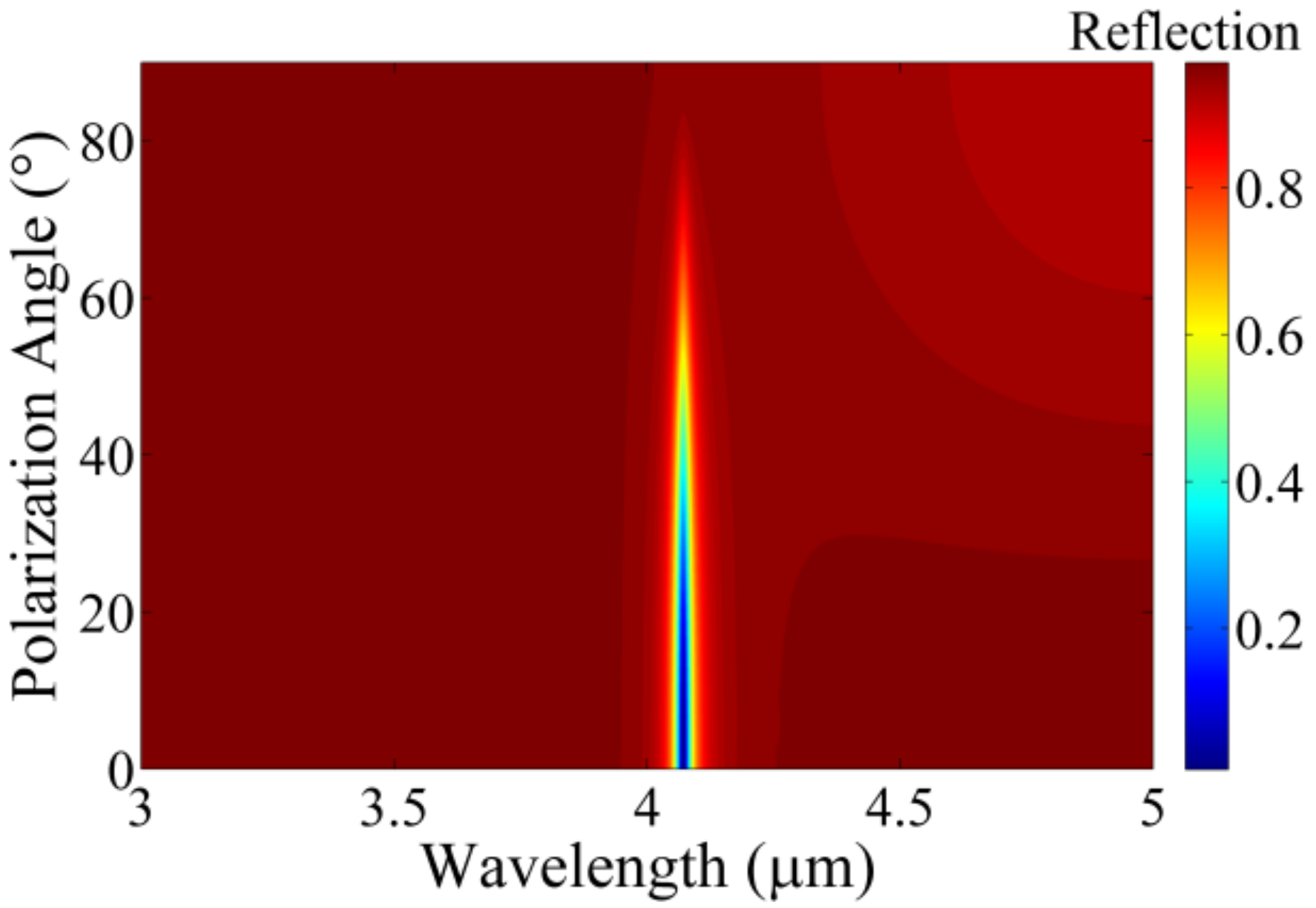
Figure 6 shows the reflection spectra at a normal incidence when adjusting the polarization angle. The polarization of the incident beam was changed from 0 degrees (TM-polarized) to 90 degrees (TE-polarized) by an interval of 2 degrees. We can see that the extinction of the reflection dip decreased with an increased polarization angle. This implies that the absorption rate at λ = 4.071 μm reduces with an increased polarization angle. This is easy to understand, since the grating in our structure was a two-dimensional grating and was polarization sensitive. However, if the polarization angle was <18 degrees, the reflection dip still had a good intensity extinction (>10 dB). This shows that our structure had a good polarization tolerance.
When our structure was used as a refractive index sensor, the simulated performance is illustrated in Figure 7. As the surrounding index increased, the resonance wavelength increased, and a quasi linear response was observed. We can obtain that the sensitivity S = Δ λ / Δ n was ~3130 nm/RIU and the figure of merit FOM = S / FWHM was ~103. Of particular note is that the resonance peak still existed in the case of a high surrounding index (>2.0), as shown in the inset of Figure 7. This reveals that, compared with those in the literature [17,26,27], the proposed sensor has the obvious advantage of still being effective in high-index surroundings.
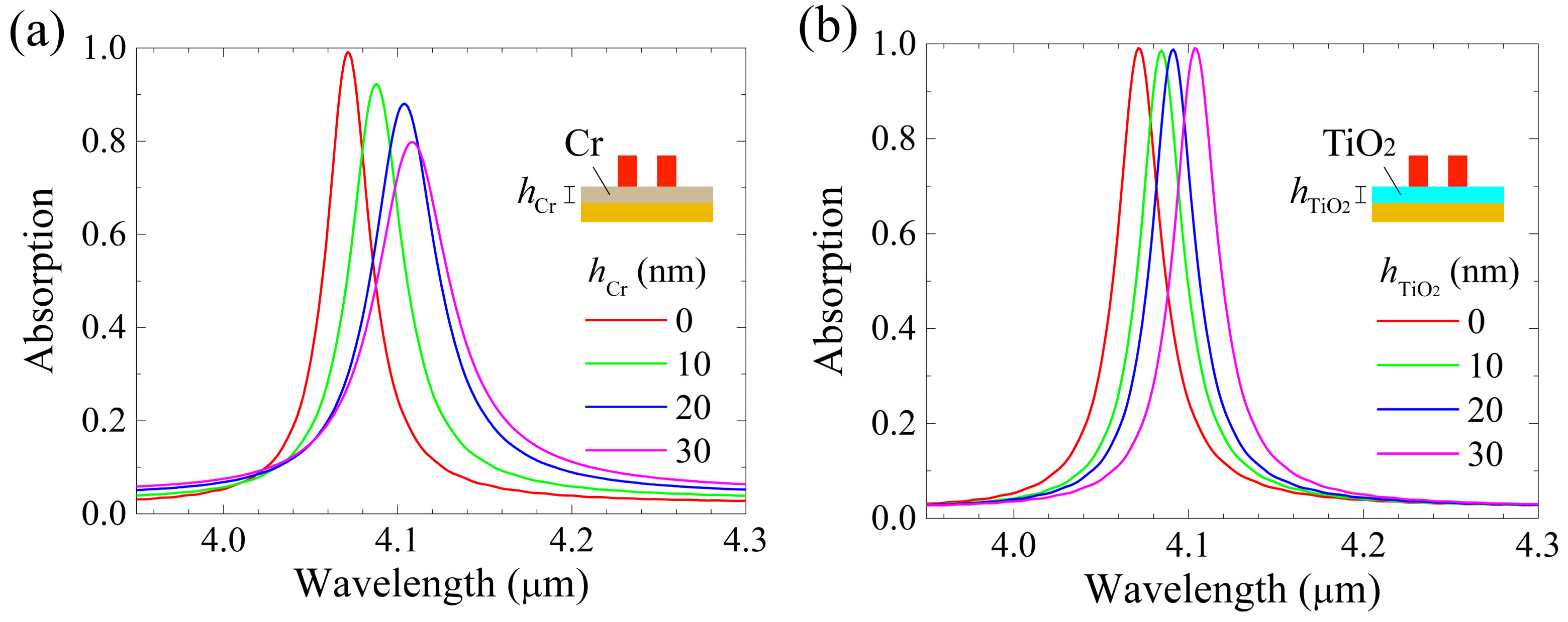
We also investigated the influence of the adhesion layer on the performance of our structure. Two kinds of materials, Cr and TiO2, were taken into account for the adhesion layer. Figure 8 shows the simulated absorption spectra with different thicknesses of the adhesion layer. In the simulations, the optical parameters of Cr and TiO2 from [32,35] were used. The other structure parameters were kept unchanged. As shown in Figure 8a, as the thickness of the Cr layer increased, the absorption bandwidth increased slightly, whereas the absorption on resonance decreased significantly. As shown in Figure 8b, with the increased TiO2 layer thickness, both the absorption bandwidth and the absorption on resonance were almost unchanged. These results suggest that the use of a TiO2 adhesion layer would be advantageous for the fabrication of the proposed structure.

5. Conclusions

We designed a mid-IR narrowband absorber based on a subwavelength fine-structured silicon–gold metagrating. It was constructed of a silicon grating on a stack of a gold film and a substrate of quartz. The grating consisted of two periodically arranged silicon strips in each unit cell. FDTD simulations indicated that perfect absorption of the TM-polarized light at a wavelength of 4.071 μm can be achieved, with an absorption rate of ~99.2% and an absorption bandwidth of ~31 nm. The structure can be used as a narrowband mid-IR notch filter operating in the reflection mode. The obtained narrow absorption peak results from the low-loss resonance mode. When the structure is used as a refractive index sensor, its measuring range can be 1.0–2.0 with a quasi linear response. The sensing FOM can be ~103, which benefits from the electromagnetic field outside the silicon strips. Although only numerical investigations were carried out in this work, the proposed absorber is simple in structure, and is potentially useful in many applications such as optical filtering, spectroscopic sensing, and gas detection.

Author Contributions

Conceptualization, X.H.; software, X.H. and J.J.; formal analysis, X.H.; investigation, X.H.; resources, J.J.; data curation, J.J. and J.Y.; writing—original draft preparation, Y.H. and S.Z.; writing—review and editing, J.Y.

Funding

This research was funded by National Natural Science Foundation of China, grant number 60907003, 61671455, 61805278; Program for New Century Excellent Talents in University, grant number NCET-12-0142; China Postdoctoral Science Foundation, grant number 2018M633704.

Conflicts of Interest

The authors declare no conflict of interest.

References

  1. Rosenberg, J.; Shenoi, R.V.; Vandervelde, T.E.; Krishna, S.; Painter, O. A multispectral and polarization-selective surface-plasmon resonant midinfrared detector. Appl. Phys. Lett. 2009, 95, 161101. [Google Scholar] [CrossRef]
  2. Li, C.; Fan, H.; Dai, Q.; Wei, Z.; Lan, S.; Liu, H. Multipole resonance in arrays of diamond dielectric: a metamaterial perfect absorber in the visible regime. Nanomaterials 2019, 9, 1222. [Google Scholar] [CrossRef] [PubMed]
  3. Liu, N.; Mesch, M.; Weiss, T.; Hentschel, M.; Giessen, H. Infrared perfect absorber and its application as plasmonic sensor. Nano Lett. 2010, 10, 2342–2348. [Google Scholar] [CrossRef] [PubMed]
  4. Liu, Y.; Zhong, R.; Lian, Z.; Bu, C.; Liu, S. Dynamically tunable band stop filter enabled by the metal-graphene metamaterials. Sci. Rep. 2018, 8, 2828. [Google Scholar] [CrossRef] [PubMed]
  5. Mason, J.A.; Smith, S.; Wasserman, D. Strong absorption and selective thermal emission from a midinfrared metamaterial. Appl. Phys. Lett. 2011, 98, 241105. [Google Scholar] [CrossRef]
  6. Vafapour, Z.; Ghahraloud, H. Semiconductor-based far-infrared biosensor by optical control of light propagation using THz metamaterial. J. Opt. Soc. Am. B 2018, 35, 1192–1199. [Google Scholar] [CrossRef]
  7. Yi, Z.; Liang, C.; Chen, X.; Zhou, Z.; Tang, Y.; Ye, X.; Yi, Y.; Wang, J.; Wu, P. Dual-band plasmonic perfect absorber based on graphene metamaterials for refractive index sensing application. Micromachines 2019, 10, 443. [Google Scholar] [CrossRef]
  8. Vafapour, Z. Polarization-independent perfect optical metamaterial absorber as a glucose sensor in food industry applications. IEEE Trans. Nanobiosci. 2019, 18, 622–627. [Google Scholar] [CrossRef]
  9. Keshavarz, A.; Vafapour, Z. Thermo-optical applications of a novel terahertz semiconductor metamaterial design. J. Opt. Soc. Am. B 2019, 36, 35–41. [Google Scholar] [CrossRef]
  10. El-Gohary, S.H.; Choi, J.M.; Kim, N.-H.; Byun, K.M. Plasmonic metal-dielectric-metal stack structure with subwavelength metallic gratings for improving sensor sensitivity and signal quality. Appl. Opt. 2014, 53, 2152–2157. [Google Scholar] [CrossRef]
  11. Lu, X.; Zhang, L.; Zhang, T. Nanoslit-microcavity-based narrow band absorber for sensing applications. Opt. Express 2015, 23, 20715–20720. [Google Scholar] [CrossRef] [PubMed]
  12. Feng, R.; Qiu, J.; Cao, Y.; Liu, L.; Ding, W.; Chen, L. Wide-angle and polarization independent perfect absorber based on one-dimensional fabrication tolerant stacked array. Opt. Express 2015, 23, 21023–21031. [Google Scholar] [CrossRef] [PubMed]
  13. Wu, D.; Liu, Y.; Li, R.; Chen, L.; Ma, R.; Liu, C.; Ye, H. Infrared Perfect Ultra-narrow band absorber as plasmonic sensor. Nanoscale Res. Lett. 2016, 11, 483. [Google Scholar] [CrossRef] [PubMed]
  14. Elshorbagy, M.H.; Cuadrado, A.; Alda, J. High-sensitivity integrated devices based on surface plasmon resonance for sensing applications. Photonics Res. 2017, 5, 654–661. [Google Scholar] [CrossRef]
  15. Kuznetsov, A.I.; Miroshnichenko, A.E.; Brongersma, M.L.; Kivshar, Y.S.; Luk’yanchuk, B. Optically resonant dielectric nanostructures. Science 2016, 354, 846. [Google Scholar] [CrossRef]
  16. Sharon, A.; Glasberg, S.; Rosenblatt, D.; Friesem, A.A. Metal-based resonant grating waveguide structures. J. Opt. Soc. Am. A 1997, 14, 588–595. [Google Scholar] [CrossRef]
  17. Liao, Y.-L.; Zhao, Y. An ultra-narrowband absorber with a dielectric-dielectric-metal structure based on guide-mode resonance. Opt. Commun. 2017, 382, 307–310. [Google Scholar] [CrossRef]
  18. Ren, Z.; Sun, Y.; Lin, Z.; Wang, C. Ultra-narrow band perfect metamaterial absorber based on dielectric-metal periodic configuration. Opt. Mater. 2019, 89, 308–315. [Google Scholar] [CrossRef]
  19. Cui, Y.; He, Y.; Jin, Y.; Ding, F.; Yang, L.; Ye, Y.; Zhong, S.; Lin, Y.; He, S. Plasmonic and metamaterial structures as electromagnetic absorbers. Laser Photonics Rev. 2014, 8, 495–520. [Google Scholar] [CrossRef]
  20. Han, D.; Wu, F.; Li, X.; Xu, C.; Liu, X.; Zi, J. Transmission and absorption of metallic films coated with corrugated dielectric layers. Appl. Phys. Lett. 2006, 89, 091104. [Google Scholar] [CrossRef]
  21. Meng, Y.; Zhang, R.-Y.; Zhang, Q.; Liu, Z.; Wu, X.; Xiao, J.; Xiang, H.; Han, D.; Wen, W. Surface plasmon polaritons on the thin metallic film coated with symmetrical and asymmetrical dielectric gratings. J. Phys. D Appl. Phys. 2017, 50, 485101. [Google Scholar] [CrossRef]
  22. Shen, S.; Forsberg, E.; Han, Z.; He, S. Strong resonant coupling of surface plasmon polaritons to radiation modes through a thin metal slab with dielectric gratings. J. Opt. Soc. Am. A 2007, 24, 225–230. [Google Scholar] [CrossRef] [PubMed]
  23. Li, X.; Han, D.; Wu, F.; Xu, C.; Liu, X.; Zi, J. Flat metallic surfaces coated with a dielectric grating: excitations of surface plasmon-polaritons and guided modes. J. Phys. Condens. Matter 2008, 20, 485001. [Google Scholar] [CrossRef]
  24. Lu, X.; Zhang, T.; Wan, R.; Xu, Y.; Zhao, C.; Guo, S. Numerical investigation of narrowband infrared absorber and sensor based on dielectric-metal metasurface. Opt. Express 2018, 26, 10179–10187. [Google Scholar] [CrossRef] [PubMed]
  25. Fitio, V.M.; Bobitski, Y.V. Resonance effects in a dielectric grating; total absorption of electromagnetic waves by a dielectric grating on metal system. J. Opt. A Pure Appl. Opt. 2004, 6, 943–951. [Google Scholar] [CrossRef]
  26. Liao, Y.-L.; Zhao, Y.; Zhang, X.; Zhang, W.; Chen, Z. An ultra-narrowband TE-polarization absorber with a dielectric grating and metal substrate. Mod. Phys. Lett. B 2017, 31, 1750306. [Google Scholar] [CrossRef]
  27. Liao, Y.-L.; Zhao, Y.; Zhang, X.; Chen, Z. An ultra-narrowband absorber with a compound dielectric grating and metal substrate. Opt. Commun. 2017, 385, 172–176. [Google Scholar] [CrossRef]
  28. Tittel, F.K.; Richter, D.; Fried, A. Mid-infrared laser applications in spectroscopy. In Solid-State Mid-Infrared Laser Sources—Topics in Applied Physics; Sorokina, I.T., Vodopyanov, K.L., Eds.; Springer: Berlin, Germany, 2003; Volume 89, pp. 458–529. [Google Scholar]
  29. Consolino, L.; Cappelli, F.; De Cumis, M.S.; De Natale, P. QCL-based frequency metrology from the mid-infrared to the THz range: A review. Nanophotonics 2019, 8, 181–204. [Google Scholar] [CrossRef]
  30. Hodgkinson, J.; Tatam, R.P. Optical gas sensing: a review. Meas. Sci. Technol. 2013, 24, 012004. [Google Scholar] [CrossRef]
  31. He, X.; Jie, J.; Yang, J.; Chen, Y.; Han, Y.; Zhang, S. Suppressing the unwanted resonance mode in a metal-insulator-metal structure using fine-structured gratings. Opt. Express 2019, 27, 15298–15308. [Google Scholar] [CrossRef]
  32. Palik, E.D. Handbook of Optical Constants of Solids; Academic Press: Chestnut Hill, MA, USA, 1998. [Google Scholar]
  33. Smith, D.R.; Schultz, S.; Markoš, P.; Soukoulis, C.M. Determination of effective permittivity and permeability of metamaterials from reflection and transmission coefficients. Phys. Rev. B 2002, 65, 195104. [Google Scholar] [CrossRef] [Green Version]
  34. Liu, X.; Starr, T.; Starr, A.F.; Padilla, W.J. Infrared spatial and frequency selective metamaterial with near-unity absorbance. Phys. Rev. Lett. 2010, 104, 207403. [Google Scholar] [CrossRef] [PubMed] [Green Version]
  35. Polyanskiy, M.N. Refractive Index Database. Available online: https://refractiveindex.info (accessed on 5 November 2019).
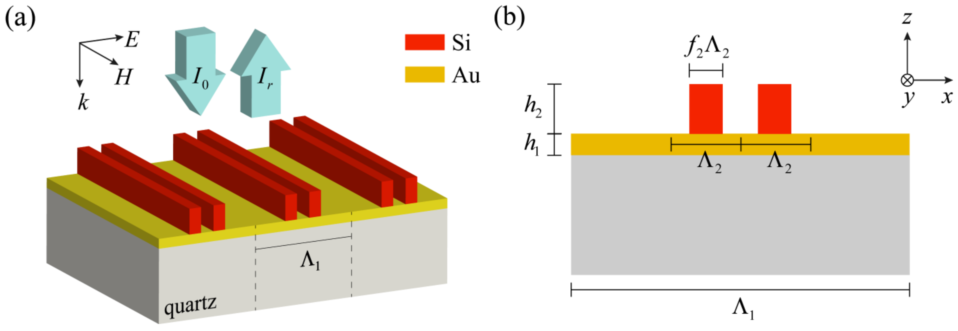
Figure 1. (a) Schematic view of the narrowband perfect absorber (PA). I 0 and I r stand for the intensities of the incidence and reflection. Λ 1 stands for the structure period. (b) Cross-sectional view of the unit cell.
Applsci 09 05022 g001
Figure 2. Simulated reflection (R), transmission (T), and absorption (A) spectra at normal incidence.
Applsci 09 05022 g002
Figure 3. (a) Retrieved optical constants for the designed narrowband PA. (b) Electric field (map) and displacement current (arrow) distributions. (c) Magnetic field distribution. (d) Energy dissipation (in W/m3). Note that the vertical dashed line in (a) and the profiles in (bd) are at λ = 4.071 μm. The electromagnetic field and displacement current distributions in (b,c) are self-normalized, respectively. The color of the arrows in (b) represents the intensity of the displacement current.
Applsci 09 05022 g003
Figure 4. Reflection as a function of (a) the grating height h 2 , (b) the sub-period Λ 2 , (c) the sub-filling-factor f 2 , and (d) the structure period Λ 1 . In (d), Λ 2 is also adjusted to keep 2 Λ 2 / Λ 1 unchanged.
Applsci 09 05022 g004
Figure 5. (a) Reflection as a function of the incident angle. Inset shows the incident plane, and θ is the incident angle. The horizontal dashed lines marked by (I) and (II) are corresponding to incident angles of 2.4 degrees and 3.8 degrees, respectively. (b) Reflection spectra associated with the two cases (I) and (II) in (a).
Applsci 09 05022 g005
Figure 6. Transmission versus the polarization angle. Traverse-magnetic (TM) polarization corresponds to 0 degree.
Applsci 09 05022 g006
Figure 7. Resonance wavelength (red circle) versus refractive index of the surrounding. A linear fit (blue line) is also shown. Inset shows the associated reflection map.
Applsci 09 05022 g007
Figure 8. (a) Simulated absorption spectra with different thicknesses of the Cr adhesion layer. (b) The same as (a) but the adhesion layer is TiO2.
Applsci 09 05022 g008