Abstract
DC microgrids are composed of loads, renewable sources, and storage devices that require control and protection to operate safely. The flyback converter is an alternative to connect paralleled batteries with nominal voltage DC buses; however, until now, complex controllers have been proposed, making difficult their implementation. On the other hand, when the voltage of a DC microgrid is not properly controlled, the loads may be damaged due to the voltage outside of the safe range. Therefore, proposed in this paper are two adaptive PI-structures to control a battery charger based on a flyback converter to be used in DC microgrids. The first adaptive current controller regulates the magnetizing current for stabilizing the system, and the second adaptive voltage controller regulates the voltage of the DC bus to protect the elements of the microgrid. The methodology to design the adaptive parameters of the PI-structures is developed as follows: first, the power stage of the flyback converter is introduced to derive a control-oriented model. The battery and the DC bus of the microgrid, which are interfaced by the flyback converter, are represented with widely accepted approaches. The second step is focused on modeling the system. The flyback converter, which includes a capacitance to model the DC microgrid, is represented by a dynamic model. The differential equations are averaged, and several transfer functions of the main variables are obtained. In the third step, the transfer functions are used to design the PI adaptive current controller and the PI adaptive voltage controller. In the last step, several recommendations are made to implement the power and control stages in low-cost hardware. An application example with realistic parameters is carried out in PSIM to validate the controller loops design. A battery of 12 V is connected to a DC microgrid of 48 V through a flyback converter with a switching frequency of 50 kHz. The settling time and deviation of the DC microgrid voltage, after a perturbation, are 0.845 ms and 2.04 V respectively, while the maximum values are adjusted to be 1 ms and 2.4 V. The simulation results validate the proposed procedure and the effectiveness of the PI-structures in regulating the magnetizing current and the DC bus voltage.
1. Introduction
Energy storage systems (ESSs) are essential elements in AC and DC microgrids (MGs) since they compensate for the unbalances between generation and load produced by unpredictable renewable energy sources, like photovoltaic and wind turbine generators [1,2,3]. Although there are different ESSs technologies, like batteries, supercapacitors, flywheels, superconducting magnetic energy storage, pumped hydro, among others [4], batteries have established as the most widely used ESS technology. Lithium-ion batteries are particularly important since they correspond to of the 5 GW energy storage capacity installed in 2020, according to the International Energy Agency [5].
In DC MGs, the battery, or array of batteries, are connected to the DC bus through a charging/discharging system, which is formed by two main elements: a bidirectional DC/DC converter and a control system. On the one hand, the DC/DC converter couples the battery voltage () to the DC bus voltage () levels, where the common relation between and is given by [1,6]; hence, step-up DC/DC converters are typically used to implement a charging/discharging system [1,6]. On the other hand, the control system is aimed at regulating the DC voltage charging or discharging the battery when the power produced by the sources is higher or lower than the load, respectively. Therefore, the battery and the charging/discharging system compensate for the unbalances between generation and load by regulating the DC bus voltage [1,2]. Such regulation is important for the correct operation of the MG, since the loads may be disconnected or damaged if is out of the expected operating range.
In the literature it is possible to find charging/discharging systems implemented with different bidirectional converters like Boost [6,7], Buck-Boost [8,9], Cuk [10,11], Zeta/Sepic [12], Sepic/Zeta [13,14], or flyback [15]. The Boost converter has some advantages like its simplicity, reduced number of components, and simple control system, regarding Buck-Boost, Cuk, Zeta/Sepic, and Sepic/Zeta. Meanwhile, these last three converters stand out due to their capacity of operating as step-up or step-down converters and lower input (Cuk and Sepic/Zeta) or output (Zeta/Sepic) current and voltage oscillations regarding the Boost converter [16]. Nevertheless, these four converters (Boost, Buck-Boost, Cuk, Zeta/Sepic, Sepic/Zeta) have limited voltage gains; consequently, must be close to , which is achieved by connecting batteries in series. The connection of batteries in series may result in imbalances in their state-of-charge due to differences in the active material and internal resistance resulting from the manufacturing process, as well as differences in the charging/discharging currents and operating temperature [17,18]. These differences may produce the overcharge or undercharge of the individual batteries, which reduces the batteries’ lifetime [18,19].
The flyback converter has the advantage of providing high voltage gains by modifying the turn ratio of its transformer, which allows the connection of a battery, or array of parallel batteries, directly to the DC bus—thus avoiding the connection of the batteries in series and reducing the unbalances among the state-of-charge of the batteries. Moreover, the flyback converter has a simple structure and provides galvanic isolation between the battery and the load. That is why this converter is used in the charging/discharging system proposed in [15] and the converter considered in this paper.
The controller for the flyback-based charging/discharging proposed in [15] is an adaptive Sliding-Mode Controller (SMC), whose main objective is to regulate the DC bus voltage. The SMC switching function is defined as , where is the reference value of , is an estimation of the magnetizing current, is the DC bus current, and and are two controller’s constants. The constant is dynamically calculated from , , the transformer turn ratio, and the transformer inductances (i.e., magnetizing and leakage) to ensure the system stability; while is a fixed value calculated to obtain the desired dynamic behavior of . Nevertheless, the controller proposed in [15] results in a variable switching frequency of the MOSFETs, which makes difficult the converter design as well as the design and implementation of filters for the measured signals. Moreover, the implementation of the hysteresis band usually requires analog circuitry, which increases the number of components required to implement the controller.
Although there is no other flyback-based charging/discharging system proposed in the literature, to the best knowledge of the authors, it is possible to find flyback-based battery charging or discharging systems with controllers simpler than SMC that provide fixed-frequency operation. For example, the authors of [20,21,22] use PI controllers for different applications that use a flyback converter to charge [20,21] or discharge a battery [22]. Particularly, in [20,21,22] the authors use a single PI to regulate the flyback output voltage for three different applications: charging an auxiliary battery for a MG, charging the battery of a phone [20], and feeding a LED light system [22]. However, these papers do not provide general design procedures that can be applied for other applications, since in [20] the authors determine the PI’s proportional gain () and the integral time () by testing three different arbitrary values for each parameter, while in [21,22] the authors do not provide any design procedure of and .
The solutions proposed in [23,24] have the same structure as the ones introduced in the previous paragraph, but they use a two-poles/two-zeros compensator instead of a PI, and the flyback output voltage is regulated to feed a DC motor. In both papers, the compensator’s parameters are designed to obtain the desired frequency response in a particular operating point of the system.
Other papers report cascade PIs to regulate the flyback output voltage to implement an electric vehicle battery charger [25,26], where the flyback input voltage is regulated by another converter with an independent controller. The cascade controller proposed in these papers has an inner loop with a PI that tracks a reference of the current injected to the battery, while the outer loop is a PI that regulates the flyback output voltage by manipulating the reference of the inner loop. In [26] the authors use frequency response to determine and of both PIs to obtain a stable system for a particular operating point. Nevertheless, in [25] the authors do not provide any design procedure for the proposed controllers.
The linear controllers for flyback-based charging or discharging (i.e., one direction of power flow) systems described before are designed for a single operating point with fixed controller parameters. Therefore, those controllers cannot guarantee the same dynamic performance of the system for any operating condition. Moreover, the papers that use linear controllers do not provide a detailed design procedure to determine the controllers’ parameters, which makes difficult their application for a charging/discharging system power flows in both directions of the converter. Additionally, the SMC controller proposed in [15] provides a variable switching frequency of the converter, which makes it difficult to design the converter and filters, and requires analog circuitry for its implementation.
This paper proposed a cascade linear controller with adaptive parameters for a flyback-based charging/discharging system along with a detailed design procedure of the controller’s parameters. In the cascade controller, the outer loop regulates the DC bus voltage by manipulating the magnetizing current reference, whereas the inner loop tracks such reference by modifying the duty cycle. The inner loop is implemented with a proportional controller with an adaptive gain () to guarantee that the closed-loop crossover frequency is of the switching frequency (F); while the outer loop is realized with a PI with two adaptive parameters ( and ), where assures a damping ratio equal to 1 whilst is designed to fulfill the desired settling time, a maximum deviation, and a closed-loop crossover frequency less than . The paper includes a detailed design procedure for the three controller parameters and guarantees the same dynamic performance of the DC bus voltage for any operating condition. Therefore, the main contributions of the paper are: (1) a cascade controller implemented with two adaptive linear compensators that guarantee the system stability and the desired dynamic performance for any operating point and mode (i.e., charging, discharging, or null); (2) a detailed design procedure of the cascade controller parameters (, , and ) considering the system stability and the bandwidth restrictions of the inner and outer loops; (3) a flyback-based charging/discharging system that operates at a constant switching frequency with an adaptive linear controller, which facilitates the design of the converter as well as the controller implementation.
The rest of the paper is organized as follows: Section 2 introduces a control-oriented model of the system, the description of the proposed cascade controller, and the design procedure. Section 3 shows an application example of the proposed design procedure, which illustrates that the system is stable and show the same dynamic performance for different operating conditions. Section 4 closes the paper with the conclusions.
2. Proposed Cascade Controller and Design Procedure
This section begins with the description of the charging/discharging system considered in this paper along with its main elements. Such description is used afterward to explain the control-oriented model used for the analysis and design procedure of magnetizing current controller. With the inner controller designed, the section continues with the system model assuming a controlled magnetizing current, which is used to analyze the DC bus voltage adaptive PI regulator and its design procedure. This section closes with a summary of the proposed controller design procedure to help the reader with its implementation.
2.1. Circuital Interface
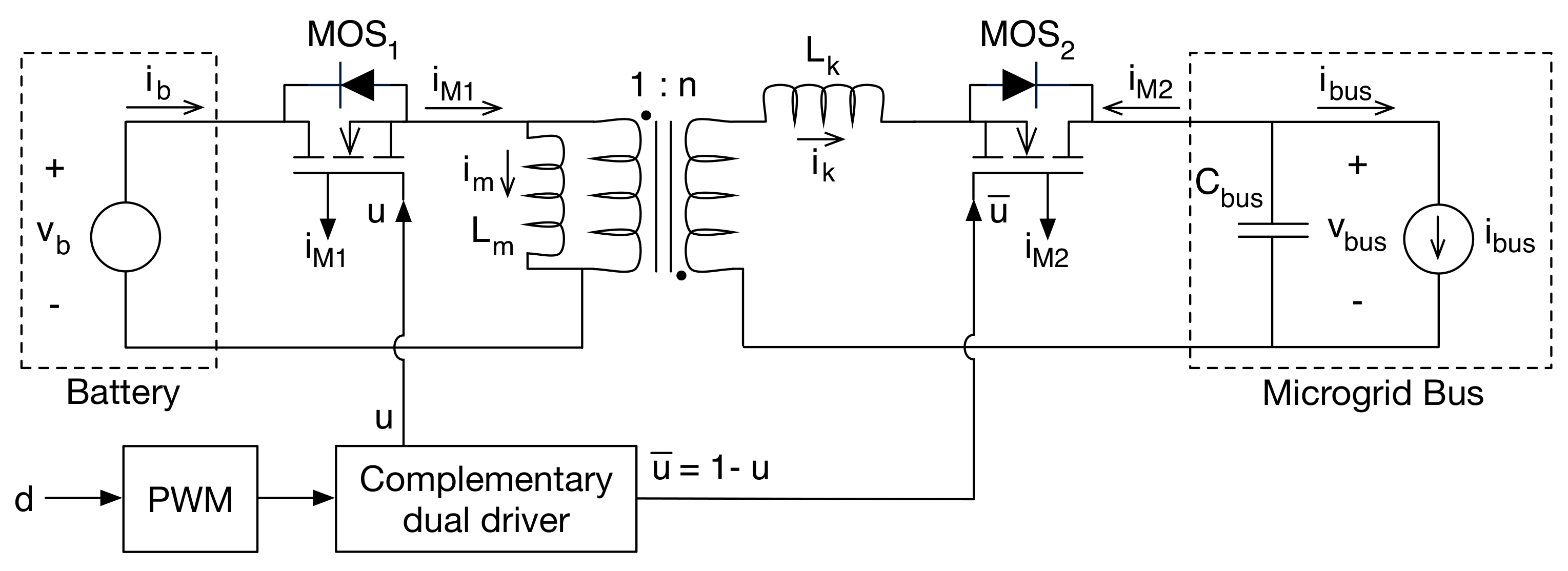
The power electronics interface proposed for this application is based on a bidirectional implementation of a flyback converter. The main advantages of this converter are the galvanic isolation, which protects the battery from failures occurring on the DC bus due to problems on the devices of the MG; and the variable voltage conversion ratio, which enables to develop a single solution suitable for multiple MGs with different bus voltage requirements.
A simplified model of the battery interface application is presented in Figure 1, which shows the flyback converter modeled with an ideal transformer with a turn ratio interacting with both the magnetizing () and the leakage () inductances. Such a power converter is designed with two complementary MOSFETs ( and ) to enable the bidirectional power flow between the battery and the bus; moreover, those MOSFETs are activated using a complementary dual driver, such as the UC1715 Complementary Switch FET Driver [27], which produces the complementary activation signals u for and for . The control signal of this power circuit is the duty cycle d of the converter, thus a PWM circuit is included in the circuital interface of Figure 1. The MOSFETs are selected to have built-in current sensing capabilities, which are needed to implement the control structure of the battery interface. Some examples of those MOSFETs are the BUK7908-40AIE [28], BUK7107-55AIE [29], and IMZ120R045M1 [30], which have TrenchPLUS current sensing circuits; and the IRCZ24 [31] that has HEXSence internal current sensors. Finally, the capacitance of the bus is labeled as , which must be designed depending on the MG requirements as will be discussed in Section 2.4.
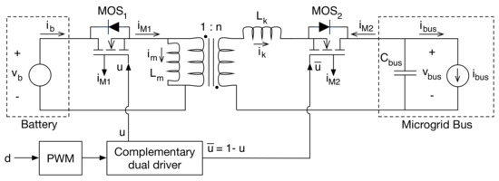
Figure 1.
Flyback-based circuital interface for bidirectional power flow.
The circuital interface of Figure 1 models the battery with the voltage source , and the MG bus is modeled with the capacitance and the current source , which combines the currents provided by the sources and consumed by the MG loads. Finally, the circuital interface has the following sensors for control purposes: the MOSFETs currents and , the battery voltage , the bus voltage , and the current exchanged with the bus , which could be positive (discharge mode), negative (charge mode), or zero (null mode).
This circuital interface must be controlled, by imposing an appropriate duty cycle, to provide a regulated bus voltage, which ensures a safe operation of the devices forming the MG. The following sections deal with the design of such a controller.
2.2. Control-Oriented Model
The correct design of the bus voltage controller requires a control-oriented model of the circuital interface, which is developed in this subsection.
The first state of the circuital interface occurs when (thus ), which produces the following equations for the bus voltage , magnetizing current , leakage current , MOSFETs currents and :
Similarly, the second state of the circuital interface occurs when (thus ), which produces the following equations:
Those equations are averaged within the switching period T of the PWM using the duty cycle definition , where is the switching frequency:
In stable conditions the previous derivatives are equal to (or near) zero, which leads to the following stable values for the duty cycle and magnetizing current:
The next step to obtain a control-oriented model is to summarize the averaged differential Equations (9) and (10) into the following matrix format:
For this circuital interface, the states vector and the inputs vector are defined as given in (17), which produces the and matrices reported in (18) and (19), respectively.
Matrices and depend on the outputs defined for the system. Since the main objective is to regulate the bus voltage to ensure a safe operation of the MG, thus, the first option is to define , which produces the matrices and . Then, applying the matrix-to-transfer function transformation , where s is the Laplace variable and I is the identity matrix, leads to the following transfer function:
The previous transfer function has a right-hand zero (RHZ), i.e., a positive zero; hence, a feedback linear-loop for a power converter designed with such a transfer function will be unstable as discussed in [32]. Therefore, the voltage in this type of system is commonly regulated using cascade structures with an inner current controller as it is discussed in [25,26], which avoids the problem of the RHZ if it is not present in the current-to-duty cycle transfer function.
To design an inner current controller, it is necessary to obtain the transfer function. Thus, the output vector is defined as , which produces the matrices and . Then, applying the matrix-to-transfer function transformation leads to the following transfer function:
Such a transfer function (21) does not have RHZ because all the terms in the numerator are positive (including ); thus, it is possible to design a stable current loop for the flyback converter using a linear controller. The transfer function is rewritten as given in (22) to reduce the mathematical expressions, where and given in (23) describe the zero, and given in (24) describes the poles. It must be noted that expression uses the steady value previously obtained in (14).
Finally, the previous , , and values must be evaluated at the operating point in which the MG is operating. Therefore, the following sections propose adaptive controllers, which are automatically modified to compensate for the changes on , , and .
2.3. Adaptive Current Controller
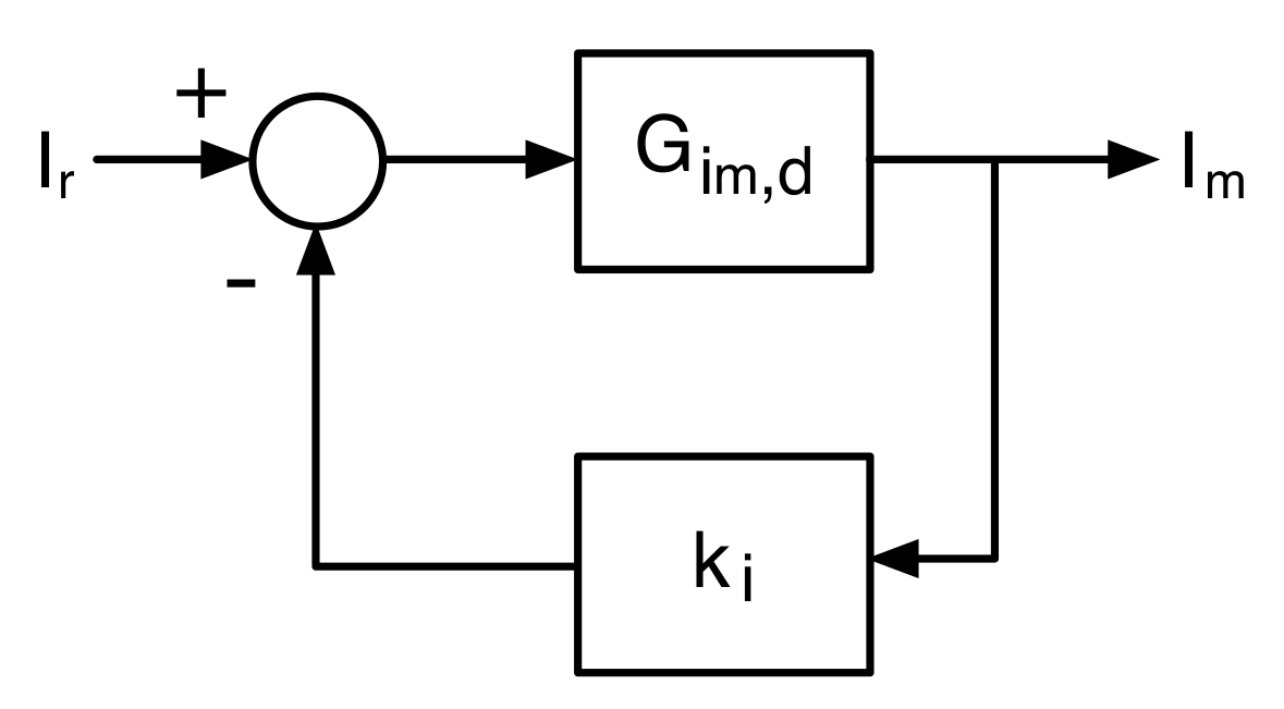
The design of the current controller is performed using the transfer function given in (22); thus, the duty cycle d is generated to regulate the magnetizing current . This process is carried out adopting the feedback structure presented in Figure 2, where the proportional controller is located in the feedback loop.

Figure 2.
Current loop based on a proportional controller.
The design of the value requires the calculation of the closed-loop transfer function , which describes the behavior of for changes on the reference value . Applying block diagram algebra to Figure 2 leads to the following transfer function for the current loop:
Taking into account that the magnetizing current is not the main variable intended to be controlled, the only restriction applied to is to constrain the transfer function gain at the maximum frequency in which the averaged model (21) accurately represents the circuit behavior. The gain of the transfer function, given as a function of the angular frequency, is reported in (26).
The bandwidth of the closed loop transfer function must be restricted to the bandwidth of the model used for the control design, otherwise the closed-loop system will operate in a frequency range in which the converter has not been modeled. In [33] it was confirmed the validity of the averaged model of a switching converter at 1/5 of the switching frequency (F), thus that is the bandwidth adopted for the design of . Therefore, Equation (26) must be solved for a gain of −3 dB , which is assumed as a cut-gain of transfer functions, thus solving for an angular frequency results in the following expression:
Therefore, the value must be dynamically calculated, using (27), to ensure the desired behavior of the current controller for any operating condition. Taking into account that , , and depend on , , and , such variables must be measured to update periodically the value, thus adapting the current controller to the operating conditions imposed by both the battery and MG.
Finally, the steady-state gain of the current loop transfer function (25) must be calculated, since such gain affects the stable value of the magnetizing current as . Therefore, such an gain must be included in the model designed to develop the bus voltage controller, which is analyzed in the following section. The value is calculated by evaluating (26) for as follows:
It must be noted that the final value was calculated by replacing the and values given in (23) and (24), respectively, and using the value updated with Equation (27). Therefore, the value is also an adaptive quantity.
2.4. Adaptive Voltage Controller
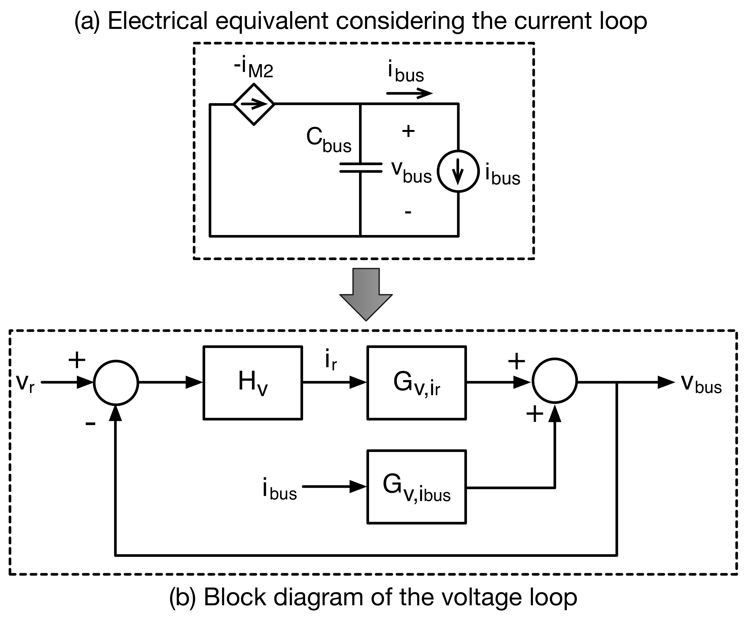
The next step needed to design the bus voltage controller is to obtain a closed-loop model of the circuital interface including the current control loop. The electrical equivalent of the flyback converter considering the current loop is presented in Figure 3a, where the average current of the second MOSFET is regulated by the current loop, which imposes the value reported in Equation (12) with .
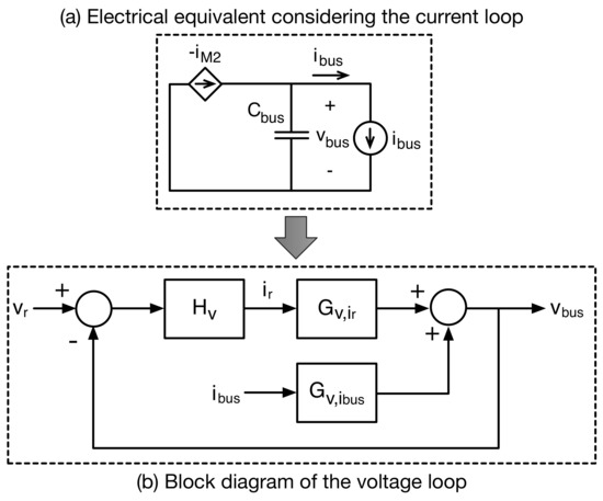
Figure 3.
Voltage loop based on a cascade controller.
Applying the Kirchhoff current law and capacitor differential equation to the circuit of Figure 3a, in the Laplace domain, leads to the bus voltage equation given in (29). Such an expression depends on both the reference current and bus current , where the latter one corresponds to the main perturbation of the system. From such an expression, two transfer functions are defined: given in (30), which describes the behavior of to changes on the current reference ; and given in (31), which describes the behavior on to perturbations on the bus current .
Figure 3b shows the block diagram of the cascade voltage loop, which considers a voltage controller named . Such a voltage controller processes the error between the voltage reference and the bus voltage to produce the reference of the current loop. Thus, the output of the voltage controller is the input of the transfer function , while bus current is the input of the transfer function . Finally, the bus voltage is the result of the contribution of both and .
This work proposes the design of a classical PI controller for as given in (32), where is the proportional parameter and is the integral parameter.
Applying block diagram algebra to Figure 3b leads to the transfer function for the voltage loop given in (33), which describes the effect of perturbations on the bus voltage . Thus, the design of parameters must be performed using such a transfer function. However, it is noted that the transfer function coefficients depend on both and d, which change with the operating point. Therefore, parameters and must be adapted to ensure consistent behavior of the bus voltage.
The adaptation of and is performed by normalizing those values concerning both and d, obtaining the normalized parameters and as given below:
Then, replacing the normalized parameters (34) into the bus voltage transfer function (33) leads to the normalized closed-loop transfer function given in (35), which exhibits constant coefficients, thus a consistent behavior of the bus voltage could be ensured.
The controller design must be performed for the worst perturbation possible on the bus current, which corresponds to a step current with an arbitrary amplitude ; thus, in the Laplace domain, it is . Then, evaluating the bus voltage from the normalized transfer function (35) considering the previous step current on the bus results in the following Laplace expression:
Considering the canonical second-order denominator enables to obtain the expressions for the natural frequency and damping ratio of the previous transfer function, as follows:
To provide a bus voltage without oscillations, the damping ratio is defined as . Then, replacing such value in (37) results in the following relation between and :
Replacing the previous relation into expression (36), and applying the inverse Laplace transformation, leads to the time-domain waveform of the bus voltage given in (39), which is the response of the voltage loop to the worst-case perturbation .
The design of the voltage controller is performed to impose the following performance criteria:
- Maximum settling time needed to restore the bus voltage into an acceptable band . In engineering, the most commonly used band for the settling time is , but any other value can be used depending on the MG requirements.
- Maximum bus voltage deviation after the bus current perturbation occurs.
- Finally, in [33] was confirmed that the validity of the current loop model on a cascade voltage control structure, like the one modeled in Figure 3, is limited to 1/5 of the current loop bandwidth. Therefore, since the current loop bandwidth was limited to , the cut-gain frequency of the transfer function (36) must be limited to 1/25 of the switching frequency; thus, a maximum angular frequency must be ensured.
For the first performance criterion, i.e., the settling time, Expression (39) is solved for and by using the LambertW function (W), which provides the expression of as a function of the controller parameter and bus capacitance :
For the second performance criterion, i.e., the maximum deviation, Expression (39) is derived as given in (41), which enables to find the time needed to reach the maximum voltage deviation that occurs when ; Equation (42) provides the expression for .
Finally, replacing the previous value on the bus voltage Equation (39) provides the expression of as a function of the controller parameter and bus capacitance :
The third performance criterion is calculated by first obtaining the magnitude of (35) depending on the angular frequency as given in (44). Then, solving that equation for the dB magnitude, thus , provides the expression of the cut-gain frequency as a function of the controller parameter and bus capacitance , which must be lower or equal than as given in (45).
Finally, the maximum acceptable setting time and bus voltage deviation are defined depending on the operational requirements of the sources and loads connected to the MG. Therefore, the non-linear equation system given in (46) must be solved to calculate both the controller parameter and bus capacitance needed to ensure the correct operation of the MG.
2.5. Summary of the Design Procedure
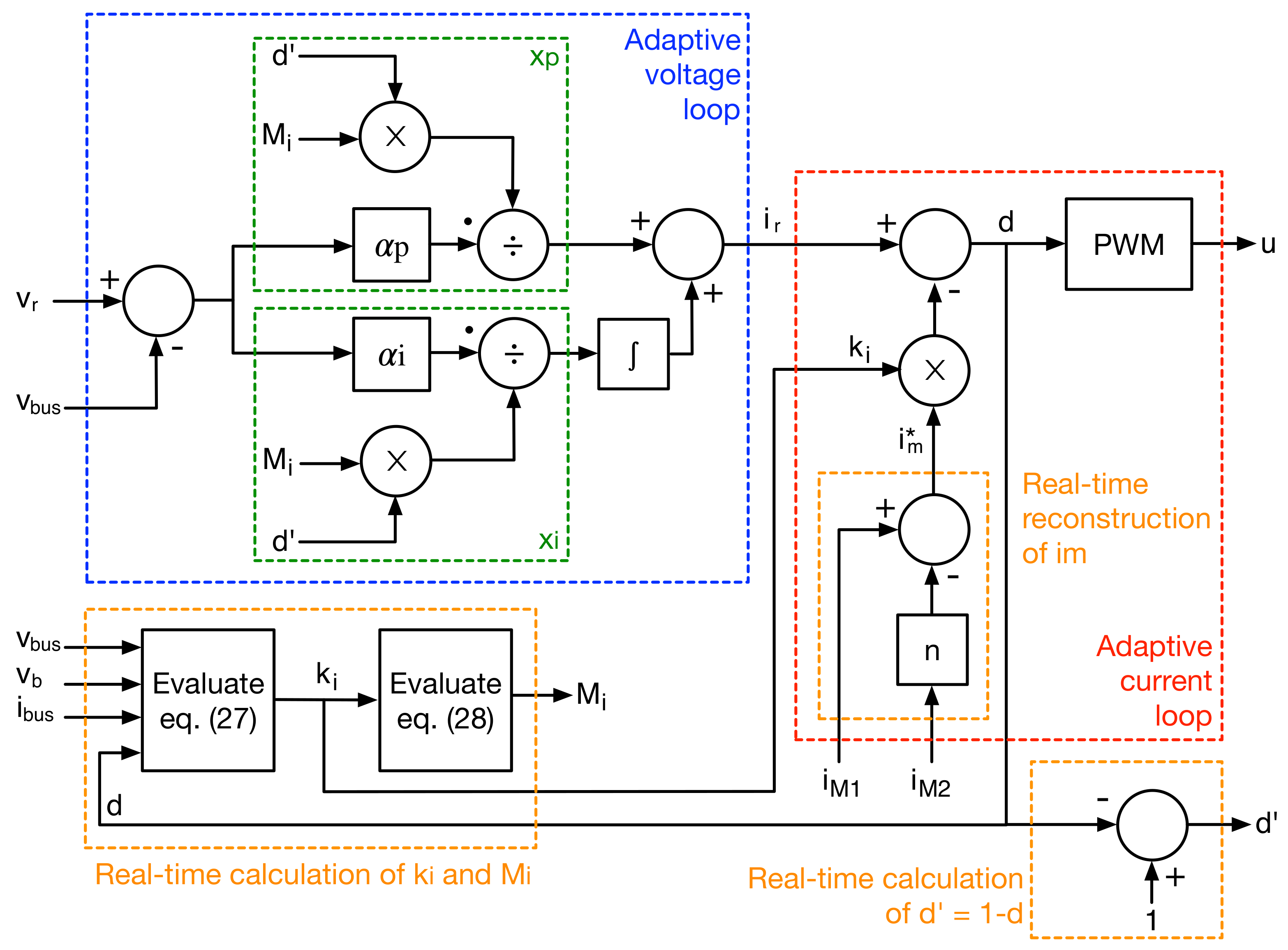
Figure 4 summarizes the offline process needed to design both the voltage controller parameters ( and ) and the bus capacitance (). Such a design process must be performed a single time since the adaptability of the control system will compensate for the changes in the operating point. The figure also summarizes the online process needed to adapt both the current and voltage loops to the changes on the operating point; this process must be performed in real-time, using analog or digital circuitry, to ensure that the controller parameters always have the correct values.
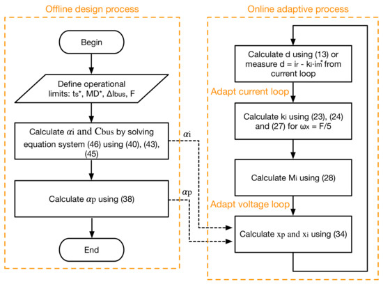
Figure 4.
Flowchart of both design and adaptive processes.
3. Results and Discussion
This section introduces the validation of the proposed controller and its dynamic performance by using an application example for a battery charging/discharging system. The section begins with a description of the implementation of the proposed controller, including the estimation procedure of the magnetizing current and the online calculation of the adaptive controller’s parameters (, , and ). Then, the section shows the dynamic performance of the proposed controller beginning with the magnetizing current for charging, discharging, and null operating modes. Finally, the section introduces an example of the design procedure of the DC voltage regulator and shows that the dynamic behavior meets the desired criteria (, , and ) for the different operating conditions.
3.1. Implementation of the Adaptive Control System
The implementation of the proposed control system is performed using Equations (27) and (28) for real-time calculation of and , respectively; Equation (34) is used for the real-time calculation of the adapted PI parameters and ; the feedback structure described in the block diagram of Figure 2 is used to implement the adaptive current loop, and the feedback structure described in the block diagram of Figure 3b is used to implement the adaptive voltage loop. Such an implementation scheme is depicted in Figure 5.

Figure 5.
Implementation of the double-adaptive control system.
Moreover, the calculation of and requires the value ; thus, such a calculation must be also performed in real-time. Finally, the current loop requires the value of the magnetizing current , which cannot be directly measured; instead, the magnetizing current must be reconstructed from the MOSFETs built-in current sensors, which were discussed in Section 2.1 and Figure 1. Such a reconstruction of the magnetizing current is based on Equations (4) and (7), as given in (47), which is also considered in the implementation scheme of Figure 5.
Considering that Equations (27) and (28) require a lot of non-linear calculations, those expressions are most suitable to be processed with a digital microprocessor. Instead, the PI calculations (integration and addition) could be done using analog circuitry like operational amplifiers. On the other hand, the calculation of and requires divisions and multiplications, which can be done using digital or analog circuits; however, taking into account that Equations (27) and (28) must certainly be calculated using a microprocessor, and can be calculated inside the same microprocessor. The same approach can be applied to the calculation of . By contrast, the reconstructed magnetizing current must be calculated using analog circuitry (operational amplifiers), since the current loop must be calculated as fast as possible. Finally, the duty cycle calculated by the current loop is delivered to the PWM, which interacts with a complementary dual-driver to act on both MOSFETs as discussed in Section 2.1.
3.2. Application Example and Validation
This subsection presents an application of the proposed solution using realistic parameters, which enables the validation of the proposed control strategy and design process. The main parameters of the application example are given in Table 1, which defines the switching frequency, battery and bus voltages, bus current range, and maximum bus current perturbation. In addition, the example considers a maximum safe deviation of the bus voltage equal to 5% (2.4 V), and a maximum 2% settling time equal to 1 ms. Finally, the transformer adopted for this application is the Vitec 58PR6962 [34], which is widely adopted in high-frequency converters [35].

Table 1.
Parameters of the application example.
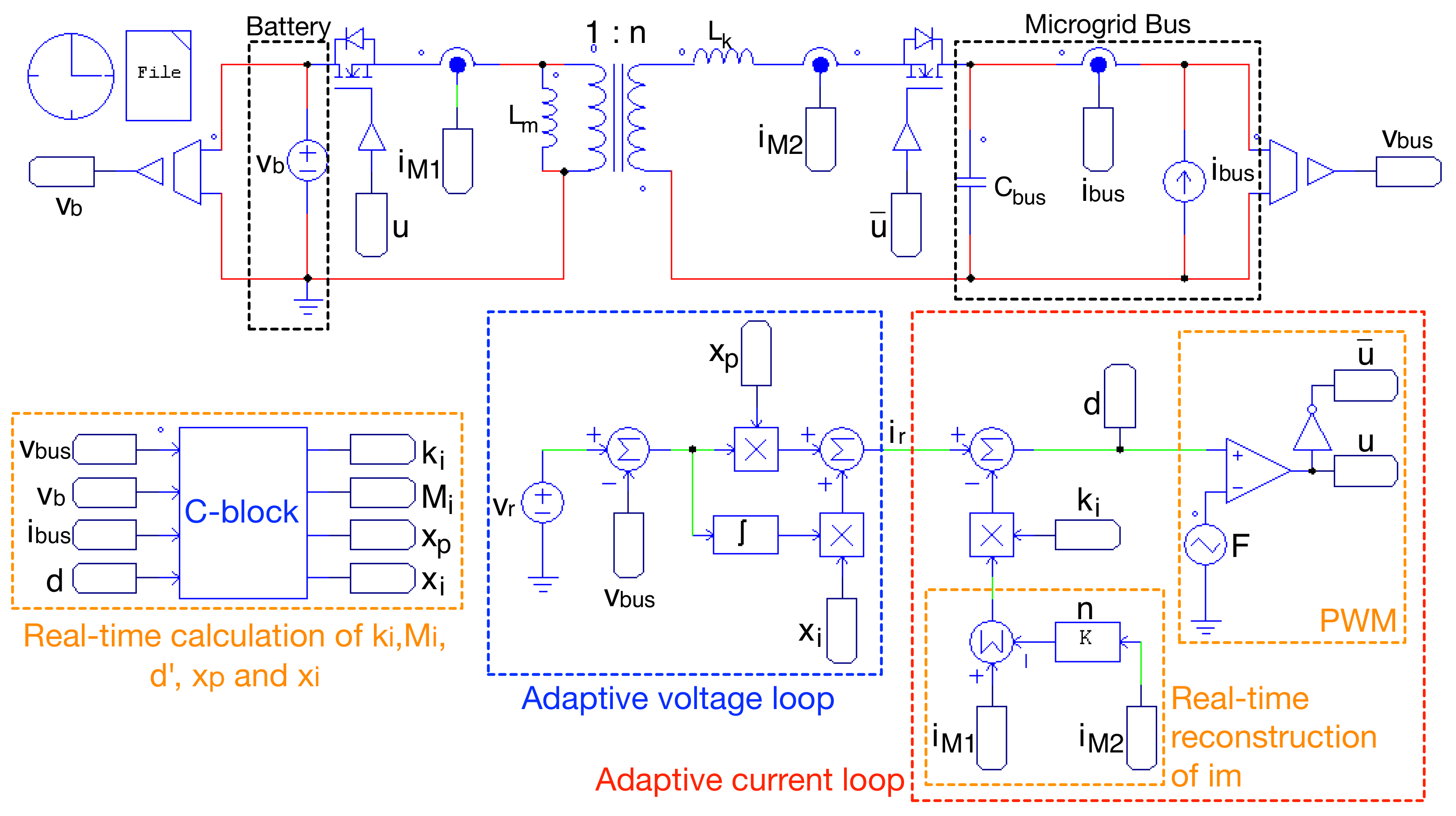
The validation of the proposed control system is performed using the professional power electronics simulator PSIM [36], which is widely used in the industry. Figure 6 shows the circuital implementation in PSIM of both power and control systems, which includes the real (non-linear) behavior of the MOSFETs, and both the magnetizing and leakage effects of the high-frequency transformer. Therefore, such a simulation tests the proposed control system under realistic conditions.
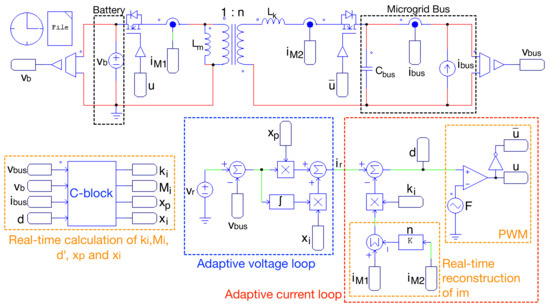
Figure 6.
Circuital implementation in PSIM of both power and control systems.
In such a circuital implementation, the calculation of , , , , and is performed in real-time using a C-block. That a block is useful to simulate digital microprocessors programmed in C language, such as the TMS320F28335 from Texas Instruments [37], where the C code used to program the C-block can be used, without any major change, to program the digital microprocessor. This is possible due to the C-block uses ANSI C; hence, it is highly portable to other platforms.
Figure 6 also highlights the circuital implementation of both adaptive loops, including the reconstruction of the magnetizing current and the PWM circuit. Moreover, the power circuit includes two current sensors simulating the MOSFETs current sensing capabilities; and the bus current is simulated using a current source, which can be modified to simulate the MG current flow generated by the interaction of the devices (sources and loads) connected to the bus. Such a circuital implementation is used to perform two tests: the first one only evaluates the current loop—thus, the voltage loop is disconnected; the second one evaluates the complete control system—thus, both current and voltage loops are active.
The first simulation considers the adaptive current loop designed in Section 2.3 following a pre-defined reference, which enables the validation of the correct adaptation of even without the action of a voltage controller, i.e., with a non-regulated bus voltage. Figure 6 shows, in the red box, the PSIM implementation of the adaptive current loop; however, in this first simulation is generated by a programmable source followed by a kHz low-pass filter, which restricts the bandwidth up to 1/5 of the switching frequency to fulfill the design given in (27). Figure 7 reports the PSIM circuital simulation of the adaptive current loop for three reference values (), where is multiplied by the loop gain (28) to validate the accurate regulation of the magnetizing current .
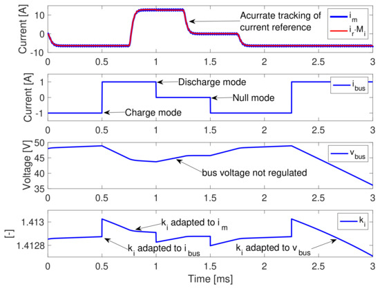
Figure 7.
Circuital simulation of the adaptive current loop in PSIM for arbitrary values of .
The simulation of Figure 7 confirms the correct regulation of the magnetizing current, which is achieved by adapting to changes in the bus current, bus voltage, and magnetizing current. Moreover, the simulation also verifies the correct operation of the current loop for charge mode, discharge mode, and null mode, therefore confirming the correct behavior under any operating condition. The next step is to design the parameters of the adaptive voltage loop.
The normalized parameters and and the bus capacitance are calculated following the flowchart previously presented in Figure 4: solving the system of nonlinear equations reported in that flowchart, using the and values given in Table 1, producing the solution spaces reported in Figure 8. In particular, Figure 8a shows the values of both and needed to ensure a maximum deviation lower than , while Figure 8b shows the values of those parameters needed to ensure a settling time lower than . Those figures provide the solution of (46) including the limitation of the voltage loop bandwidth to F/25 defined in (45), thus ensuring the stability of the voltage loop. From Figure 8a,b can be selected particular and values to define precise and conditions; in this example, a commercially available F capacitance is selected, thus providing a 17% safe margin for the maximum deviation. Similarly, A/(V · s) is selected to provide a 15% safe margin for the settling time.
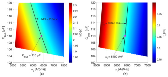
Figure 8.
Plots used to design of and . (a) Design of in terms of . (b) Design of in terms of .
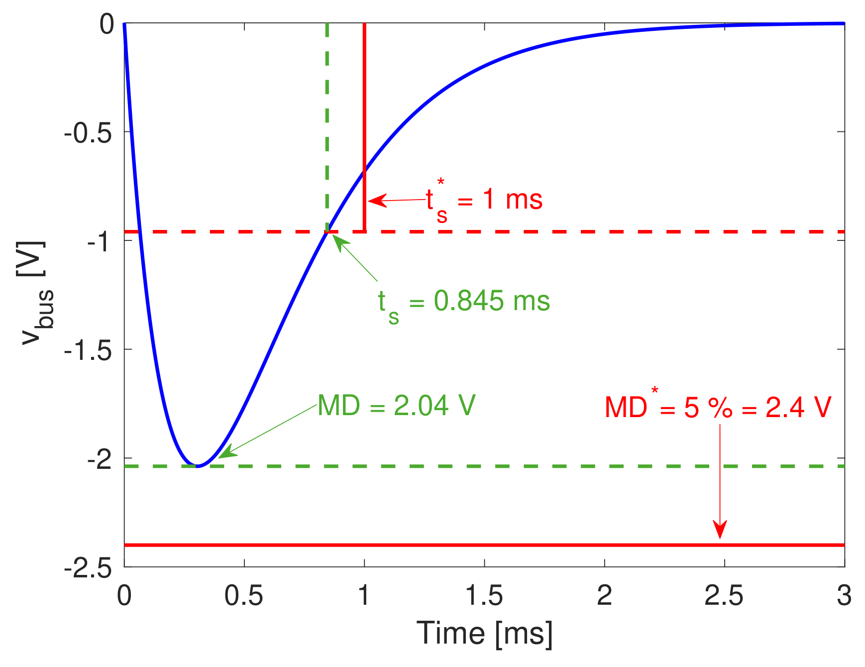
Figure 9 shows the theoretical simulation of the bus voltage using the normalized waveform given in (36), where A/V is calculated from (38). The figure confirms the accurate definition of both the settling time ms and maximum deviation V, thus verifying the correctness of the design procedure summarized in the flowchart of Figure 4.

Figure 9.
Theoretical simulation of the normalized voltage controller.
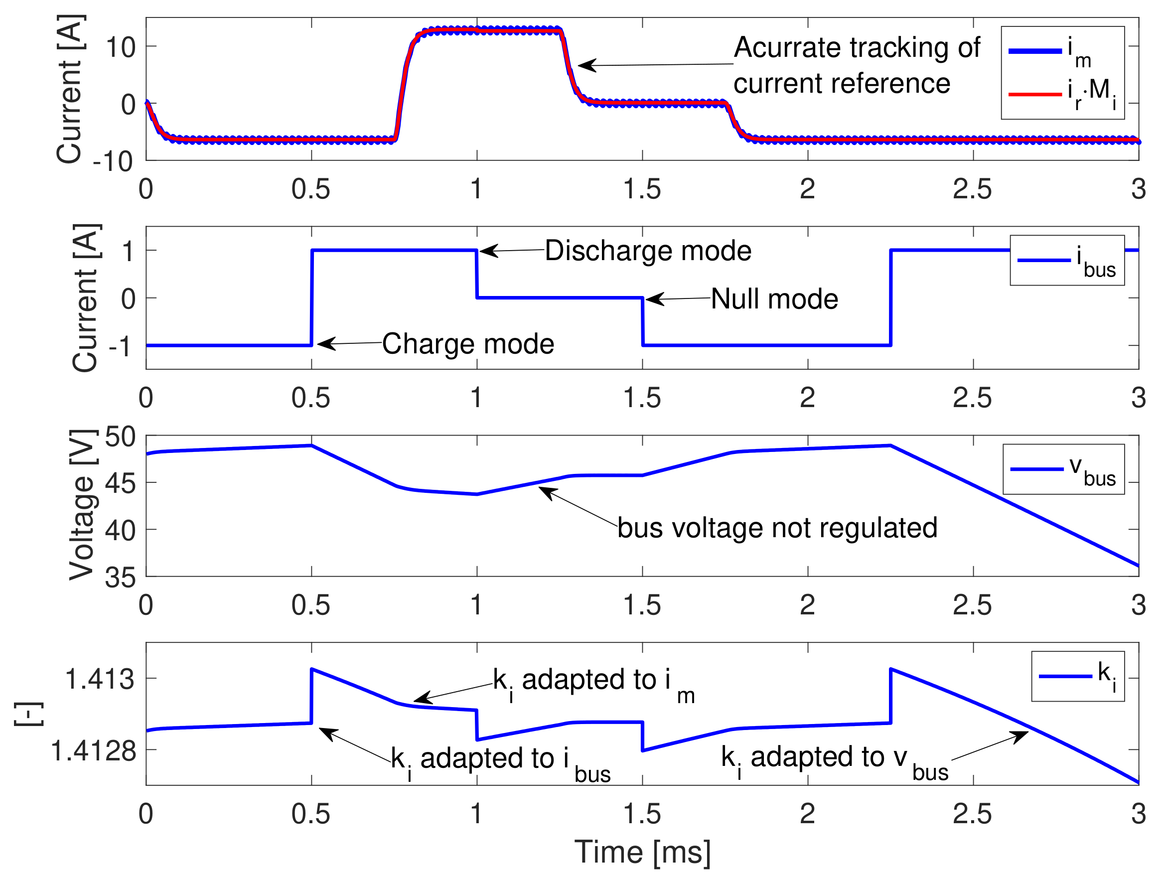
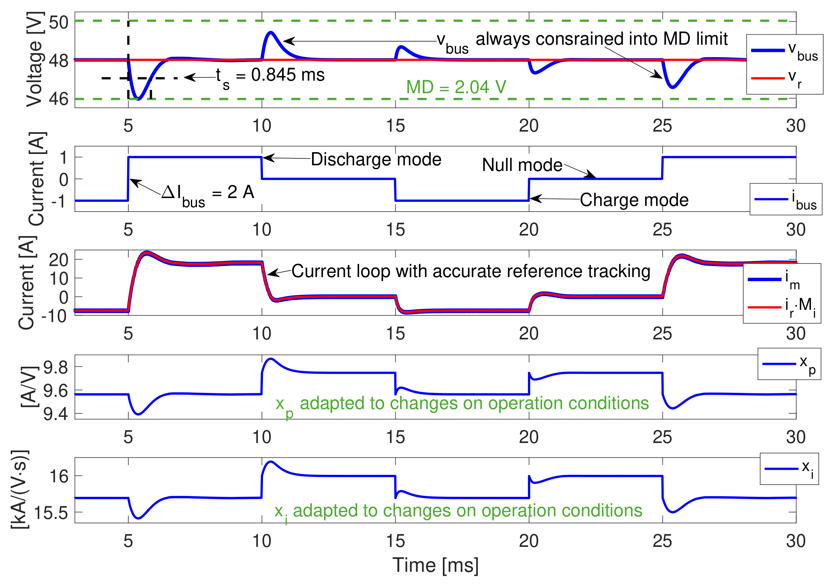
Finally, Figure 10 reports the complete PSIM simulation of the double adaptive PI-structure, which corresponds to the circuital implementation of Figure 6 including the adaptive voltage loop. This simulation considers a bus current profile with charge, discharge, and null conditions to evaluate the control system for all the possible conditions. The first step perturbation in the bus current has A as reported in Table 1, and the simulation shows a settling time ms and a maximum voltage deviation V, which is in agreement with the design parameters selected from Figure 8 and with the theoretical results reported in the normalized simulation of Figure 9. Therefore, this circuital simulation confirms the validity of both the design process and the practical implementation reported in Figure 6. Moreover, the bus current also exhibits step changes for both charge and discharge conditions, where the bus voltage is always lower than ; therefore, and are always below the maximum limits defined in Table 1, i.e., % and ms, which ensures a safe operation of all the devices connected to the MG.

Figure 10.
Circuital simulation of the double adaptive PI structure in PSIM.
The simulation of Figure 10 also shows the correct operation of the adaptive current loop, since the magnetizing current is always equal to the theoretical value . Finally, the figure also shows the dynamic adaptation of the voltage loop parameters and , which both are modified when the bus voltage and current change. Therefore, the proposed control system always ensures the same desired performance for any operating condition, which is the main objective of the proposed control system.
4. Conclusions
DC MGs are a suitable approach to connect loads, renewable sources, and storage devices to produce electric energy. Loads, sources, and storages devices can be interconnected through power converters that can be used to guarantee a safe operation of the elements and consequently for the entire MG. A formal design of a battery charging/discharging solution based on a flyback converter and two adaptive control loops were proposed in this paper to protect the devices of a DC MG. The design was dominated by a formal procedure that modeled the system and establish three performance criteria to be guaranteed by the controllers: a maximum settling time, a maximum voltage deviation, and a maximum angular frequency. The PI structures are adaptive to changes in the operating point, even for changes in the converter parameters. To encourage the interested community to implement the battery charging solution, a detailed design flowchart was presented. In addition, several recommendations were made to select the hardware that can be used in the implementation of the battery charger and its controllers. Hence, this paper provides three main contributions: (1) an adaptive linear controller that guarantees the system stability and the desired dynamic behavior for any operating condition; (2) a step-by-step design procedure to determine the controller parameters considering the system stability; and (3) a charging/discharging based on a flyback converter with an adaptive linear controller that operates at a fixed switching frequency.
Finally, a practical example simulated in PSIM software confirmed the correct operation of the adaptive current loop and the adaptive voltage loop. The simulation results showed that bus voltage fulfilled the performance criteria defined in the case ( ms, , and ). However, additional verifications, using real hardware, will be performed in the future to test the proposed control system under commercial conditions.
Author Contributions
Conceptualization, C.A.R.-P., A.J.S.-M. and J.D.B.-R.; methodology, C.A.R.-P., A.J.S.-M. and J.D.B.-R.; software, C.A.R.-P., A.J.S.-M. and J.D.B.-R.; validation, C.A.R.-P., A.J.S.-M. and J.D.B.-R.; writing—original draft preparation, C.A.R.-P., A.J.S.-M. and J.D.B.-R.; writing—review and editing, C.A.R.-P., A.J.S.-M. and J.D.B.-R. All authors have read and agreed to the published version of the manuscript.
Funding
This work was supported by the Universidad Nacional de Colombia and the Instituto Tecnológico Metropolitano under the research project “Microinversor de alta eficiencia para maximizar la extracción y transferencia de energía desde paneles fotovoltaicos ubicados en zonas con sombreado parcial a cargas de corriente alterna y voltaje estándar (110 V)” (Hermes code 49938, ITM code PE21103).
Institutional Review Board Statement
Not applicable.
Informed Consent Statement
Not applicable.
Data Availability Statement
The data used in this study are reported in the paper figures and tables.
Acknowledgments
The authors thank the Facultad de Minas (Sede Medellin) and Facultad de Ingeniería y Arquitectura (Sede Manizales) of the Universidad Nacional de Colombia.
Conflicts of Interest
The authors declare no conflict of interest.
References
- Zhang, Y.; Lu, Z.; Lu, Q.; Wei, S. The Research on Bus Voltage Stabilization Control of Off-Grid Photovoltaic DC Microgrid under Impact Load. Math. Probl. Eng. 2019, 2019, 8913956. [Google Scholar] [CrossRef]
- Sun, J.; Lin, W.; Hong, M.; Loparo, K.A. Voltage Regulation of DC-Microgrid with PV and Battery: A Passivity Method. IFAC-PapersOnLine 2019, 52, 753–758. [Google Scholar] [CrossRef]
- Castro, L.; Bueno-López, M.; Mora-Flórez, J. Fuzzy mathematics-based outer-loop control method for converter-connected distributed generation and storage devices in micro-grids. Computation 2021, 9, 134. [Google Scholar] [CrossRef]
- Rahman, M.M.; Oni, A.O.; Gemechu, E.; Kumar, A. Assessment of energy storage technologies: A review. Energy Convers. Manag. 2020, 223, 113295. [Google Scholar] [CrossRef]
- International Energy Agency (IEA). Energy Storage; IEA: Paris, France, 2021. [Google Scholar]
- Song, Z.; Hou, J.; Hofmann, H.; Li, J.; Ouyang, M. Sliding-mode and Lyapunov function-based control for battery/supercapacitor hybrid energy storage system used in electric vehicles. Energy 2017, 122, 601–612. [Google Scholar] [CrossRef]
- Capasso, C.; Veneri, O. Experimental study of a DC charging station for full electric and plug in hybrid vehicles. Appl. Energy 2015, 152, 131–142. [Google Scholar] [CrossRef]
- Sahín, M.E.; Okumu, H.Í.; Kahvecí, H. Sliding mode control of PV powered DC/DC Buck-Boost converter with digital signal processor. In Proceedings of the 2015 17th European Conference on Power Electronics and Applications (EPE’15 ECCE-Europe), Geneva, Switzerland, 8–10 September 2015; pp. 1–8. [Google Scholar] [CrossRef]
- Ramos-Paja, C.A.; Bastidas-Rodríguez, J.D.; González, D.; Acevedo, S.; Peláez-Restrepo, J. Design and Control of a Buck–Boost Charger-Discharger for DC-Bus Regulation in Microgrids. Energies 2017, 10, 1847. [Google Scholar] [CrossRef] [Green Version]
- Farjah, A.; Ghanbari, T.; Seifi, A.R. Contribution management of lead-acid battery, Li-ion battery, and supercapacitor to handle different functions in EVs. Int. Trans. Electr. Energy Syst. 2020, 30, e12155. [Google Scholar] [CrossRef]
- Sousounis, M.C.; Shek, J.K.; Sellar, B.G. The effect of supercapacitors in a tidal current conversion system using a torque pulsation mitigation strategy. J. Energy Storage 2019, 21, 445–459. [Google Scholar] [CrossRef] [Green Version]
- Kloenne, A.; Sigle, T. Bidirectional ZETA/SEPIC Converter as Battery Charging System with High Transfer Ratio Keywords Comparison Buck-Boost and ZETA/SEPIC Topologies. In Proceedings of the 2017 19th European Conference on Power Electronics and Applications (EPE’17 ECCE Europe), Warsaw, Poland, 11–14 September 2017; pp. 1–7. [Google Scholar] [CrossRef]
- Dimna Denny, C.; Shahin, M. Analysis of bidirectional SEPIC/Zeta converter with coupled inductor. In Proceedings of the 2015 International Conference on Technological Advancements in Power and Energy (TAP Energy), Kollam, India, 24–26 June 2015; pp. 103–108. [Google Scholar] [CrossRef]
- Gayen, P.K.; Roy Chowdhury, P.; Dhara, P.K. An improved dynamic performance of bidirectional SEPIC-Zeta converter based battery energy storage system using adaptive sliding mode control technique. Electr. Power Syst. Res. 2018, 160, 348–361. [Google Scholar] [CrossRef]
- Ramos-Paja, C.A.; Bastidas-Rodriguez, J.D.; Saavedra-Montes, A.J. Design and Control of a Battery Charger/Discharger Based on the Flyback Topology. Appl. Sci. 2021, 11, 10506. [Google Scholar] [CrossRef]
- Soedibyo; Amri, B.; Ashari, M. The comparative study of Buck-boost, Cuk, Sepic and Zeta converters for maximum power point tracking photovoltaic using P&O method. In Proceedings of the 2015 2nd International Conference on Information Technology, Computer, and Electrical Engineering (ICITACEE), Semarang, Indonesia, 16–18 October 2015; pp. 327–332. [Google Scholar] [CrossRef]
- Dubarry, M.; Devie, A.; Liaw, B.Y. Cell-balancing currents in parallel strings of a battery system. J. Power Sources 2016, 321, 36–46. [Google Scholar] [CrossRef] [Green Version]
- Omariba, Z.B.; Zhang, L.; Sun, D. Review of Battery Cell Balancing Methodologies for Optimizing Battery Pack Performance in Electric Vehicles. IEEE Access 2019, 7, 129335–129352. [Google Scholar] [CrossRef]
- Lotfi, N.; Fajri, P.; Novosad, S.; Savage, J.; Landers, R.G.; Ferdowsi, M. Development of an experimental testbed for research in lithium-ion battery management systems. Energies 2013, 6, 5231–5258. [Google Scholar] [CrossRef]
- Chao, P.C.; Chen, W.D.; Wu, R.H. A battery charge controller realized by a flyback converter with digital primary side regulation for mobile phones. Microsyst. Technol. 2014, 20, 1689–1703. [Google Scholar] [CrossRef]
- Chang, Y.C.; Liaw, C.M. Establishment of a Switched-Reluctance Generator-Based Common DC Microgrid System. IEEE Trans. Power Electron. 2011, 26, 2512–2527. [Google Scholar] [CrossRef]
- Mamizadeh, A.; Mustafa, B.A.; Genc, N. Planar Flyback Transformer Design for PV Powered LED Illumination. Int. J. Renew. Energy Res. 2021, 11, 439–445. [Google Scholar]
- Musasa, K.; Muheme, M.I.; Nwulu, N.I.; Muchie, M. A simplified control scheme for electric vehicle-power grid circuit with DC distribution and battery storage systems. Afr. J. Sci. Technol. Innov. Dev. 2019, 11, 369–374. [Google Scholar] [CrossRef]
- Huang, K.C.; Huang, S.J. Design Enhancement of a Power Supply System for a BLDC Motor-Driven Circuit with State-of-Charge Equalization and Capacity Expansion. IEEE Trans. Ind. Electron. 2018, 65, 8613–8623. [Google Scholar] [CrossRef]
- Singh, B.; Kushwaha, R. EV battery charger with non-inverting output voltage-based bridgeless PFC Cuk converter. IET Power Electron. 2019, 12, 3359–3368. [Google Scholar] [CrossRef]
- Kushwaha, R.; Singh, B. Interleaved Landsman Converter Fed EV Battery Charger with Power Factor Correction. IEEE Trans. Ind. Appl. 2020, 56, 4179–4192. [Google Scholar] [CrossRef]
- Texas Instruments. UC1715-SP UC1715-SP. 2013. Available online: https://www.ti.com/product/UC1715-SP (accessed on 6 December 2021).
- Nexperia. BUK7908-40AIE. 2009. Available online: https://assets.nexperia.com/documents/data-sheet/BUK7908-40AIE.pdf (accessed on 6 December 2021).
- PHILIPS. BUK71/7907-55AIE. 2002. Available online: https://www.mouser.com/datasheet/2/916/BUK71_7905_40AIE-04-1319113.pdf (accessed on 6 December 2021).
- Inineon. IMZ120R045M1. 2020. Available online: https://www.infineon.com/dgdl/Infineon-IMZ120R045M1-DataSheet-v02_06-EN.pdf (accessed on 6 December 2021).
- International Rectifier IOR. IRCZ24. Available online: https://www.galco.com/techdoc/vish/ircz24_dat.pdf (accessed on 6 December 2021).
- Erickson, R.W.; Maksimović, D. Fundamentals of Power Electronics, 3rd ed.; Springer: Berlin/Heidelberg, Germany, 2020; pp. 1–1071. [Google Scholar] [CrossRef]
- Petrone, G.; Ramos-Paja, C.A.; Spagnuolo, G. Photovoltaic Sources Modeling; John Wiley & Sons, Ltd.: Chichester, UK, 2017. [Google Scholar] [CrossRef]
- ViTEC. Flyback CCM Transformer 58PR6962. 2000. Available online: https://www.viteccorp.com (accessed on 6 December 2021).
- Metry, M.; Balog, R.S. An Adaptive Model Predictive Controller for Current Sensorless MPPT in PV Systems. IEEE Open J. Power Electron. 2020, 1, 445–455. [Google Scholar] [CrossRef]
- PSIM. PSIM: The Ultimate Simulation Environment for Power Conversion and Motor Control. 2021. Available online: https://www.powersimtech.com (accessed on 1 March 2022).
- Texas Instruments. TMS320F28335. 2021. Available online: https://www.ti.com/product/TMS320F28335 (accessed on 1 March 2022).


Publisher’s Note: MDPI stays neutral with regard to jurisdictional claims in published maps and institutional affiliations. |
© 2022 by the authors. Licensee MDPI, Basel, Switzerland. This article is an open access article distributed under the terms and conditions of the Creative Commons Attribution (CC BY) license (https://creativecommons.org/licenses/by/4.0/).