Review

In(Ga)N Nanostructures and Devices Grown by Molecular Beam Epitaxy and Metal-Assisted Photochemical Etching

1
Department of Physics, College of Science, United Arab Emirates University, Al Ain 15551, UAE
2
Wuhan National Laboratory for Optoelectronics, School of Optical and Electronic Information, Huazhong University of Science and Technology, Wuhan 430074, China
3
Key Laboratory of Semiconductor Materials Science, Institute of Semiconductors, Chinese Academy of Sciences & Beijing Key Laboratory of Low Dimensional Semiconductor Materials and Devices, Beijing 100083, China
4
College of Materials Science and Opto-Electronic Technology, University of Chinese Academy of Science, Beijing 101804, China
*
Authors to whom correspondence should be addressed.
These authors contributed equally to this work.
Nanomaterials 2021, 11(1), 126; https://doi.org/10.3390/nano11010126
Submission received: 11 December 2020 / Revised: 28 December 2020 / Accepted: 31 December 2020 / Published: 7 January 2021

Abstract

:
This review summarizes the recent research on nitride nanostructures and their applications. We cover recent advances in the synthesis and growth of porous structures and low-dimensional nitride nanostructures via metal-assisted photochemical etching and molecular beam epitaxy. The growth of nitride materials on various substrates, which improves their crystal quality, doping efficiency, and flexibility of tuning performance, is discussed in detail. Furthermore, the recent development of In(Ga)N nanostructure applications (light-emitting diodes, lasers, and gas sensors) is presented. Finally, the challenges and directions in this field are addressed.

1. Introduction

Group III–V semiconductors, in particular, III-nitrides and their compounds, have recently received growing interest from the scientific community owing to their fascinating fundamental properties and novel applications. The outstanding properties of these materials, including wide direct bandgap, chemical and thermal stability, piezo/pyroelectricity, high conductivity/mobility, and biocompatibility, enable reliable operation of devices together with the awareness of different environmental and ecological challenges [1,2,3,4]. Nanostructured GaN and InGaN possessing the above properties have become revolutionary materials. The flexible bandgap range from 0.64 for InN to 3.45 eV for GaN, covering a uniquely ultra-wide spectrum [1], is ideal for broader applications. Advances in the synthesis of these materials have led to major developments in practical nanoscale smart objects, such as light-emitting diodes (LEDs), probes, photovoltaics, and lasers [5,6,7,8,9]. These materials are also used as efficient photoanodes in solar-powered water splitting, which turns an alternative energy source into fuel, albeit releasing CO2 in the process [10].
Nanostructures are usually prepared using bottom–up [11,12,13] or top–down [14] approaches. Well-aligned GaN and InGaN nanostructures have been obtained by metal–organic chemical vapor deposition (MOCVD) [15,16,17], molecular beam epitaxy growth (MBE) [18], the vapor–liquid–solid (VLS) mechanism [19], laser-assisted catalytic growth (LCG) [20], and the ion-etching reaction [21,22].
In this review, we focus on MBE and metal-assisted photochemical etching (MacEtch), which can be used to grow high-quality nitride nanostructures. MBE is a popular bottom–up method for growing arsenide materials and devices [23]. In recent years, MBE has also been widely used to grow nitride nanowires under nitrogen-rich conditions with a high V/III flux ratio, which promotes vertical growth and limits lateral growth [24]. The nanowire geometry confines the possible defects to the bottom of the structure, thereby ensuring high crystal quality in the upper active region and improving light extraction in LEDs. As the strain in nanowires (unlike that in nitride thin films) can be relaxed both out of plane and in-plane from the sidewall, the indium composition of InGaN nanowires can be substantially improved without worrying about increased strain, and the strain-related piezoelectric polarization field can be reduced. Furthermore, the structure can grow on different heterogeneous substrates, such as Si, metal, and quartz [24,25,26]. Due to their high quality and large specific surface areas, nitride nanowires have been adopted in LEDs, lasers, and water-splitting applications [27,28,29].
Both bottom–up growth and dry etching techniques are expensive and complex [12,30]. By contrast, wet etching can be accomplished via a more straightforward process at a lower cost with less material damage. The wet-etching process can be easily realized in a liquid reservoir such as a beaker, with the nanostructures obtained being intact without any surface lattice damage compared with those obtained using dry etching techniques. [31]. Several GaN and InGaN nanostructures have been fabricated by wet-etching methods, mainly via electrochemical and photochemical etching. Porous n-GaN can be synthesized via electrochemical etching in acidic (HF) or alkaline solutions [32,33,34] by applying an external current. The morphology of the etched material is influenced by the character and concentration of the electrolyte [35], material doping level, illuminance power, and sample bias [36]. A possible alternative to photoelectrochemical etching is metal-assisted chemical etching, which generates porous nanowire semiconductors using electroless techniques [37]. MacEtch is the most popular technique because it produces a homogeneous porous morphology over a wide region and is simpler than other surface-roughening techniques. [38,39]. MacEtch prevents the surface damage caused by dry etching procedures, which is desired for potential optoelectronic applications. MacEtch reactions can be broadly categorized into two types: single-step reactions with HAuCl4/HF [37], AgNO3/HF [40] or solutions containing AgNO3/HF/CH4O [38]; and two-step reactions involving predeposition of metal nanoparticles or patterned thin-film metals in the presence of HF/H2O2 [41].

2. Synthesis Methods for (In)GaN Nanostructures

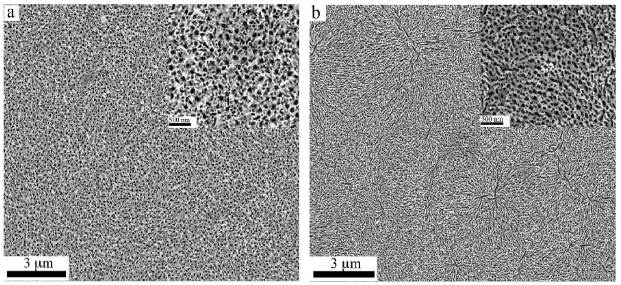
2.1. GaN and InGaN: Porous and Nanowire Structures Prepared via MacEtch

MacEtch has become a well-developed technique for preparing Si nanostructures [42,43,44,45] and has recently been adopted for synthesizing GaN nanostructures. Najar et al. [46] synthesized GaN nanowires (NWs) using MacEtch. They coated 10-nm-thick strips of platinum separated by a few millimeters on a cleaned GaN film using a sputtering system and treated the films in a solution containing H2O2:HF:CH3OH (2:1:2) under ultraviolet (UV) light. Very long NWs (>10 μm) with a wurtzite structure were obtained. Geng et al. [38] investigated the growth of porous GaN in various metal catalysts and GaN doping environments and demonstrated an improvement in the MacEtch technique and the catalytic scheme in the order of Ag < Au < Ir < Pt. The authors also observed that the catalytic action of continuous films contrasted with that of films with discontinuous islands. Continuous metal films covered the surface tightly, obstructing the MacEtch reaction. This effect can be resolved by fabricating discontinuous films or increasing the intensity of laser irradiance. Doping enhanced the MacEtch activity in the order of p-GaN < intrinsic GaN < n-GaN. Benton et al. performed photoelectrochemical etching in KOH solution, creating nanoporous GaN and InGaN/GaN films with pore sizes varying between 25 and 60 nm [47].
Najar et al. [48,49,50,51] also fabricated porous GaN nanostructures by etching bulk GaN in a solution of H2O2, CH3OH, and HF with a volume ratio 2:1:2. They found a relationship between the elastic properties and porosity kinetics of the nanostructures; in particular, the elastic modulus of the structure decreased with a decrease in porosity.
The etching time does not seem to affect the morphology and size of the resulting pores, but prolonging the etching duration increases the number of pores (see Figure 1). The approximate porosities of the samples etched for 45 and 90 min were 17.5% and 32%, respectively. The appearance of elongated pores in the 90-min etched sample was due to the fusion of cylindrical pores by the etchant, which narrowed the sidewalls between adjacent pores.
Perumal et al. [52] compared the porosifications of MacEtch-fabricated GaN in different porosification catalysts—hydrofluoric acid (HF) based (CH3OH:HF:H2O2), nitric acid (HNO3) based (CH3OH:HNO3:H2O2), sulfuric acid (H2SO4) based (CH3OH:H2SO4:H2O2), and platinum (Pt)—under UV enhancement. Under continuous UV illumination, the Pt catalyst increased the number of holes at the etchant–semiconductor interface by absorbing incident radiation, thereby increasing the etch rate. The authors formed a uniformly distributed network of nanopores with no ridge morphology. The pore size ranges of the HF, H2SO4, and HNO3-etched samples were 38–42, 42–47, and 14–18 nm, respectively (extended pores), and 18–20, 20–22, and 9–11 nm, respectively (small pores), with equivalent proportions of CH3OH and H2O2. The HNO3 etchant yielded smaller pores with excessive pore intensity, whereas the other etchants produced larger pores of similar size.
Figure 2 shows the X-ray diffraction (XRD) spectra of as-grown samples and samples obtained with various etchants. The higher crystallinity in the etched samples than in the as-grown samples, manifesting as high diffraction-peak intensity, was attributable to substrate-induced stress relaxation. The diffraction peaks at 34.59° and 76.35° are associated with the (0002) and (0004) GaN diffraction planes, respectively. Film formation was verified by the high intensity of the (0002) reflections along the c-plane. The GaN peaks of all etched samples confirmed that the GaN layer was not completely etched away and preserved its epitaxy. Zang et al. [53] produced single-crystalline, smooth-surfaced GaN nanowires (0002) via MacEtch over an electrodeposited metal catalyst (Au nanoparticles). The ideal moving path of the Au nanoparticles was along the (0002) face of GaN. GaN NWs can be many microns long, and their diameters range from 8 to 24 nm. The single peak at 34.5° in the XRD spectrum of the GaN nanowires was indexed to the (0002) wurtzite-type crystal face of GaN.
Wang et al. [54] studied the role of metal distribution in the formation of GaN nanowires and demonstrated that GaN effectively forms in AgNO3 solution or a mixed solution of CuSO4 and HF. They prepared metal-based etchants by combining concentrated AgNO3 or CuSO4 (0.01 M) with concentrated HF (5.0 M) and deionized water. The topology of the GaN surface changed significantly as the etching time increased from 10 to 50 min. The GaN film became porous after 10 min of etching under UV irradiation, and nanowires were created after 20 min of etching. Prolonging the etching time to 40 min increased the length of the nanowires.
Using MacEtch, Wang et al. [55] grew a single nanowire with a diameter of ≈25 nm and a rough surface, approaching the surface topography of Si NWs [56]. Figure 3a shows a transmission electron microscopy (TEM) image of their sample. The selected area electron diffraction pattern (Figure 3a, inset) confirmed the monocrystalline characteristics of the NWs. The enlarged image in Figure 3b clarifies the monocrystalline character of the NWs. The interplanar distance of the NWs was consistent with the c-plane lattice constant of GaN and verified the monocrystalline hexagonal structure of the NWs on the etched samples.
Unlike the traditional anodic etching techniques for fabricating porous semiconductors, MacEtch is an electroless etching technique employing an unpatterned discontinuous metal layer in a solution containing HF and H2O2. MacEtch forms porous structures of Si and III–V semiconductor materials [57,58]. To initiate open-circuit local oxidation and reduction reactions, MacEtch utilizes noble metals. The process begins when the oxidant creates holes (h+) on the metal surface and then diffuses into the semiconductor. The holes are consumed by oxidizing the semiconductor directly below the metal, forming a soluble product in the acid solution [59]. The holes are generated via oxidant reduction catalyzed by cathode materials such as Au, Cu, Ag, and Pt deposited on the semiconductor surface. When these holes are introduced to the semiconductor valence band (VB), they oxidize and establish an ionic structure soluble in an acid solution (e.g., HF). By this process, the materials are eliminated despite the net metal utilization. The etching mechanism and chemical reactions during the MacEtch process are schematically shown in Figure 4. The formation mechanisms of GaN and InGaN nanostructures are similar and hence can be generalized.
GaN and InGaN nanostructures are formed via a three-phase process. First, under UV irradiation in the presence of CH3OH:H2O2:HF (2:1:2) etching solution, electron–hole (e–h) pairs are formed at the interface of GaN or InGaN–electrolyte. Aided by band bending at the substrate–electrolyte interface, the photogenerated holes oxidize the anode reaction at the GaN or InGaN surface while the electrons diffuse into the GaN or InGaN mass. The holes act as an anode, oxidizing the surface layer of GaN and InGaN with the evolution of N2 gas, forming Ga2O3 and In2O3, respectively.
The overall etching duration plays a significant role in determining the morphology of GaN and InGaN nanostructures. In both cases, samples etched for a shorter period are porous, and further etching leads to nanowire formation. The etching of the GaN or InGaN layer leads to a porous structure resulting from epitaxial surface-layer dislocations and defects, followed by coalescing of the surface and vertical progression along the crystalline structure. After a sufficiently long etching time, the surfaces of GaN and InGaN are fully covered with vertical GaN and InGaN nanowires. As the etching time is further increased, the density of the nanowires becomes high, as seen in Figure 5b,d.
The etching mechanism, which occurs by oxidation and subsequent dissolution of the semiconductor surface, relies mainly on the photogenerated e–h pairs. Holes play a significant role in increasing the oxidation state of the surface atoms. The number of surface holes for the oxidation reaction is increased by the absorption of incident radiation. The etching process forms bubbles through the evolution of nitrogen. The etching time relies on the involvement of the surface charge region at the n-GaN–electrolyte boundary, which results from the Fermi level equilibrium between the GaN surface and the electrochemical potential of the electrolytes (see Figure 6).
The metal-assisted photochemical electroless etching of n-GaN starts when electron-hole pairs are excited by the incident UV photons. The photo-generated holes enter the interface of the GaN/electrolyte and are located at the surface bonds, allocating oxidation to the surface gallium atoms. The holes oxidize the surface layer to generate Ga2O3 gas via the evolution of N2, as seen in the following Equation (1) [62], and function as an anode.
2GaN + 6h+ + 3H2O → Ga2O3 + 6H+ + N2
The reduction reaction of H2O2 by Equation (2) occurs in platinum as the cathode for water generation.
H2O2 + 2H+ → 2H2O + 2h+
HF’s reaction to Ga2O3 is the second step. This reaction occurs on the surface of GaN crystal grains, on the boundaries of the GaN crystallite grain, and on the dislocations of the surface [63]. The Ga2O3 oxide dissolution occurs to form GaF3, as shown in Equation (3).
Ga2O3 + 6HF → 2GaF3 + 3H2O
The dissolution of Ga2O3 oxide in the HF solution will improve the baffling bonds and be responsible for the positive oxide charges under insufficient oxygen conditions [64]. Repulsion from the positive oxide surface of H+ charged ions in the solution will reduce the dissolution rate of Ga2O3 by Equation (4) on the surface of the crystal grain.
Ga2O3 + 6H+ → 2Ga3+ + 3H2O
However, dislocated sites and defects are negatively charged [64,65], and dissolution of Ga2O3 can be effectively commenced at surface defect sites at a much higher rate owing to HF [66]. Pores are formed on the GaN surface for shorter etching periods. The final phase is for longer etching times as the pores are etched in the GaN layer across the vertical (0001) crystallographic direction at the dislocation sites, leaving behind NWs structures. The GaN Nanowires then get longer and collapse after prolonging a couple of microns [54].
Depending on the local current flux and the complete disposal of the oxidized semiconductor required to maintain the local electrochemical reaction), MacEtch can produce both solid and porous nanostructures. The porosity is controlled by varying the oxidant/acid ratio in the solution and the type and design of the catalyst. The various synthesis parameters for the development of GaN and InGaN porous nanowires are given in Table 1 and Table 2, respectively. MacEtch reactions occur only at the metal–semiconductor interface in controlled etching environments. Consequently, the metal sinks into the semiconductor while the semiconductor is etched just below the metal, serving as a mask to resist etching. When the metal catalyst is shaped in any manner and length, the pattern gravitates into the semiconductor, creating microstructures and nanostructures such as pillar arrays and reverse hole structures [37]. GaN nanostructures ranging from dendritic extensions to highly monodisperse collections of GaN nanowires can be prepared by varying the solution composition, concentration, and etching time under UV illumination [40]. GaN has a more favorable VB (–6.66 eV relative to vacuum) than metals such as Au, Ag, Cu, and Pt. The UV illumination assists in hole formation in the VB during the GaN etching process. The electrons in the VB of GaN gain sufficient energy to excite the conduction band under UV illumination, creating holes in the VB simultaneously.
Najar et al. observed a redshift in the peak position of the photoluminescence (PL) spectrum of porous GaN samples [48] as shown in Figure 7a, which contrasts with the blue shift reported in porous Si nanostructures caused by quantum size effects [79]. The relief in the porous GaN samples can be related to uniaxial stress. The scattering of light from the pores’ sidewalls improves the photon removal effectiveness and decreases the dislocation density in the GaN porous structures; accordingly, the PL intensity increases with an increase in porosity. Benton et al. [47] noted a similar redshift of the emission wavelength in GaN samples. In their study, they found that the GaN epitaxial layer experienced significant compressive strain, causing a 16% lattice mismatch between GaN and its sapphire substrate. The strain could be relaxed to a large extent because of the development of the nanoporous structures, leading to a redshift in the PL peak position that depended on the extent of relaxation. Perumal et al. [52] reported a similar redshift in the near-band-edge emission peaks of their etched porous samples, which appeared at ≈363.5 nm. Evidently, the defect density in etched samples is higher than that in as-grown samples because the etching process increases the specific surface area and removes some of the nanostructures. Raman spectroscopy provides information on vibrational states that are sensitive to crystallinity, stress, carrier concentration, and mobility. Therefore, Raman spectra can be used to monitor the formation process and growth of GaN nanowires (see Figure 7b). Group theory suggests four active Raman modes in GaN nanowires, which normally crystallize into a hexagonal wurtzite structure: E2L, E2H, E1(TO), and A1(LO) [80]. Typically, the peaks of these four modes appear around 143, 658, 556, and 724 cm−1, respectively. Xi et al. performed a Raman study of GaN nanowires produced on anode aluminum oxide templates [81]. They allocated the Raman peaks at 143, 556, 568, and 733 cm−1 to the E2L, E1(TO), E2H, and A1(LO) modes of first-order phonons, respectively. A peak at 752 cm−1 emerged with a reduction in the GaN NW diameter. An acoustic phono-overtone was attached to the 315 and 418 cm−1 peaks. Under an incident laser, the high specific surface area of the NWs resulted in additional molecular vibrations that dramatically increased the strengths of the E2L, E2H, A1(LO), and E1(TO) peaks of GaN NWs from those of planar GaN. For GaN nanowires with a diameter of 60 nm, a different Raman surface mode (Frohlich mode) at ≈815 cm−1 was observed. Najar et al. observed a new Frohlich mode peak at 750.5 cm−1 in anisotropically etched GaN NWs (see Figure 7d), which they attributed to the anisotropy [46]. They noted a lower frequency shift ascribable to the stress relief that occurred during longer etching periods.

2.2. Exfoliation of Porous Structure and NWs

GaN membranes have been prepared via diverse processes: laser [82], chemical [83], electrochemical [84,85], and mechanical lift-off from suitable buffer layers [86,87]. However, the direct growth of inorganic NWs on flexible substrates is hampered by interfacial reactions between the grown nanowires and flexible metallic substrates and the low melting temperatures of flexible organic substrates [88]. Doan et al. lifted an InGaN/GaN LED from a sapphire surface using a 248-nm KrF excimer laser [89]. Chung et al. deposited a GaN LED directly on a thin-film layer of ZnO-coated graphene and mechanically lifted it from the substrate [90]. Subsequently, Kobayashi et al. mechanically lifted a GaN LED from a boron nitride buffer layer [91]. Cheng and co-workers demonstrated transferable substrate-less GaN LED grown on SiC buffer layer [92]. Voronenkov et al. removed the GaN layer by laser cutting [93]. The lifted GaN was transferred onto a copper substrate. Despite these advances, existing methods involve several steps and often require costly equipment. These limitations have impeded the further production of GaN crystal membranes. Xiao et al. synthesized self-standing nanoporous GaN membranes via electrochemical reaction and found the nanopore morphology is related to the n-doping concentration [94]. Yoo et al. [95] fabricated a GaN LED on a polyamide substrate using a standard soft lithography technique. The flexible GaN LED was mechanically and optically stable on a flexible substrate, surviving a bending test of radius up to 3.5 mm and a cycling test up to 2000 times. GaN can be transferred from sapphire to a flexible substrate by laser lift-off and contact printing [96]. A flexible GaN membrane platform on a silicon wafer developed by eutectic bonding and a laser lift-off process offers flexibility for the stable and reliable design of various pixel shapes and related manufacturing processes. Flexible GaN has also been developed using other techniques such as the selective anisotropic etching of N-polar GaN in hot phosphoric acid [97]. However, there are few reports on the preparation of flexible GaN via electrochemical etching methods. ElAfandy et al. [98] realized threading dislocation-free (TD-free) nano-membrane generated from MacEtch of GaN template-substrates, as shown in Figure 8. The threading dislocations were carefully separated during the etching process, forming nanowires, while the ~25 nm thick nanomembrane was remaining unetched on the surface of the substrate. The GaN nanomembrane, the NWs, and the porous area are visible clearly in Figure 8a,b. The microscopic picture (Figure 8c) clearly shows its flexibility. Ultralong GaN NWs were obtained as shown in Figure 8d if the etching process persists for a prolonged time.

2.3. Nitride NWs Grown by MBE

Under high-vacuum conditions, atoms of one or more types constituting an epitaxial film are sprayed as atomic beams onto the substrate. Some of the bombarded atoms form an ordered crystal film on the substrate by undergoing a physical–chemical process. The In, Ga, and Al beams (group III) are generated by thermal evaporation, whereas reactive N beams are formed by NH3 or N2 plasma, which can also be used to grow III-nitrides (important for growing In-nitride) at low temperatures. The high-vacuum chamber not only provides a long mean-free-path for the beam atoms but also promotes the development of high-quality (In, Al)GaN nanostructures without any catalyst. The growth parameters can be accurately controlled via in situ monitoring capability. Although the growth rate in MBE is low, it has proven very successful in the growth of optoelectronic device structures [99,100].
Specific substrates are required for epitaxial growth. Homoepitaxial growth is favored because it avoids thermal and lattice mismatches, which degrade the quality of the epitaxial layer. This is important for the epitaxial growth of optoelectronic device structures based on GaAs. However, in the epitaxial growth of III-nitrides, this approach is rendered difficult by the small size and high price of the GaN or AlN substrates. At present, sapphire, silicon carbide, and silicon substrates are the primary substrates for epitaxial GaN. Table 3 gives the material parameters of the III-nitride epitaxy. The lattice parameters of conventional substrates largely differ from those of GaN, leading to an elevated density of dislocations in epitaxial GaN films.
The high dislocation density has restricted the growth of GaN film on the abovementioned substrates. However, researchers have successfully grown GaN nanowires on these substrates [107]. In nanowire epitaxy, the dislocation density is reduced by the effective strain relaxation [108,109] and low polarization fields [110].
Nanowires grow by a sequential process of absorption, desorption, nucleation, and growth, as shown in Figure 9. GaN nuclei have different diameters and their locations and nucleation times are random, resulting in high dispersal. Nanowire growth is driven by Ga diffusion along the sidewalls, and the growth rate is inversely proportional to the diameter of the NWs. When the nucleus reaches a critical size, its subsequent growth is attributed to the direct incorporation of Ga atoms that hit the apex of the NWs and diffuse to the bottom of the NWs. After reaching the substrate, they climb up to the apex along the sidewall [111,112].
Using the MBE process, Yoshizawa et al. [113] grew self-organized GaN nanopillar structures on a (0001) sapphire substrate in a radio-frequency (RF)-generated radical source. The obtained nanopillars were dense along the c-axis and remained perpendicular to the growth plane. By studying the effect of the growth conditions on the nanopillars, they found that the growth rate, density, and diameter of the nanopillars increased with an increase in the N2 flow rate, and the nanopillar diameter could be increased by increasing the RF power. Therefore, the nanopillar sizes can be regulated by controlling the N2 gas flow rate and RF power [113]. Araki et al. observed that when GaN is grown on a sapphire substrate by electron cyclotron resonance MBE, H2 supports the epitaxial layer and stimulates the three-dimensional columnar growth of GaN [114]. Namkoong et al. [115] investigated the effect of nitridation temperature of the sapphire substrate on subsequent growth. Prior to the growth of GaN on sapphire, the substrate was exposed to an N2 plasma atmosphere for nitridation at 200 °C in plasma-assisted MBE. A uniform Al–N layer singularity was formed on the surface of the nitrided sapphire substrate, providing a nucleation point for the subsequent GaN growth at 500 °C. The nitridation significantly improved the crystal quality of the following layer [115].
Kikuchi et al. performed high-temperature nucleation of Al–N and self-organized growth of GaN nanopillars on a (0001) sapphire substrate after low-temperature nitridation in RF-MBE. They controlled the diameter, height, and density of the nanopillars by changing the growth conditions. The final density, average diameter, and height of the nanopillars were 2 × 1010 cm−2, 80 nm, and 1.8 μm, respectively. Figure 10 shows a scanning electron microscopy image of the nanopillars. The strong emission peaks in the PL spectrum of the GaN nanopillars confirmed their high crystal quality, which is essential for optoelectronic applications [116]. Ramesh et al. grew a vertically distributed GaN nanowall network (NWN) by applying laser-assisted MBE technology on a nitrided sapphire substrate. The high crystal quality of the GaN NWN was demonstrated by the small full-width-at-half-maximum (FWHM) in the XRD rocking curve test. Furthermore, they found that the nitridation temperature of the substrate influences the type of stress developed in the epitaxial GaN layer [117].
GaN nanostructures have also been grown on silicon substrates, which are economical and can be produced in large quantities. Kikuchi et al. developed GaN nanopillars on Si (111) substrates. Unlike the direct nitridation of sapphire substrates in an N2 plasma atmosphere, silicon substrates should be processed under a Ga beam before passing into N2 plasma to form GaN dots, which serve as the initial nucleation sites for subsequent growth. They developed GaN nanopillars with a diameter of 80–100 nm, a height of 1500-nm, and a density of 1.2 × 1010 cm−2. The threshold optical power density of stimulated emission from the obtained GaN nanopillars was as low as 300 kW/cm2 [118].
Bertness et al. produced GaN nanowires on Si (111) without metal catalysts. The nanowires were well separated, and their diameters and lengths were around 50–250 and 2–7 μm, respectively. The authors suggested that growth via this mechanism (unlike catalytic growth) depends partly on the stability of the nonpolar GaN planes [119]. Meijers and colleagues [120] studied the relationship between the morphological/optical characteristics and growth parameters of GaN NWs grown via MBE on Si (111) substrates. They found that by optimizing the equivalent pressure of the Ga beam ramp, tapering and agglomeration could be prevented. The growth was driven by self-catalysis of the Ga droplets.
Guo et al. demonstrated the catalyst-free production of InGaN NWs of diameter ranging from 10 to 50 nm with high density (1–2 × 1011 cm−2) on a (001) Si substrate, as shown in Figure 11. The NWs were crystallized into a wurtzite structure with relatively few defects compared to nitride films. The emission of the NWs could not only be tailored from UV to red but could be broadened to a white emission by changing the composition. The intrinsic quantum efficiency varied from 20% to 35%. The radiative and nonradiative lifetimes of the carriers were 5.4 and 1.4 ns, respectively. Both green- and white-emitting planar LEDs were also produced, with a relatively low quantum-confined Stark effect and bandtail filling effects [121].
Guo et al. developed GaN NWs on a silicon (111) substrate using plasma-assisted MBE, and also grew InGaN NWs at low temperatures to prevent precipitation of In. TEM images showed that the NW diameters were uniformly distributed in the radial direction, with very few dislocations; consequently, the GaN NWs delivered an excellent performance. The authors regulated the composition of the InGaN layer by changing the growth conditions during the epitaxy process, thereby changing the NW emission spectrum. In the time-resolved PL spectrum of the nanowires, the radiative recombination lifetime was higher than the nonradiative recombination lifetime, further confirming the low defect density in the NWs [121].
Mi et al. grew AlN and AlGaN NW in an RF-MBE system. The proper size and density of the AlN nanowires were achieved by controlling the GaN nanowire seed layer. As revealed in the PL emission spectrum, the properties of the AlN nanowires largely depended on the growth temperature of the initial GaN nanowires. Mg-doped AlN nanowires achieved high-efficiency p-type conduction owing to their high crystal quality. Meanwhile, the PL spectrum of the AlGaN nanowires revealed the high application potential of Al(Ga)N nanowires in UV and deep-UV luminescence [122].
Kruse et al. performed selective-area MBE growth of GaN NWs on SiO2-masked Si (111) substrates. The NWs were directly grown on the Si substrate, and an oxide mask was formed with no additional buffer or mask materials. When the diameter of the mask window was less than 50 nm, most of the NWs were straight and vertical. The diffusion length was also influenced by the window spacing; when the spacing exceeded 1 μm, the ratio of window space to unoccupied window space was almost unrelated to the window density [123].
NWs have also been developed on high-thermal-conductivity substrates. Schuster et al. developed GaN NWs and nanotubes on a diamond substrate via MBE supported by a structured Ti mask (see Figure 12). The Ga-polarity of the wurtzite NWs suppressed the parasitic growth at high substrate temperatures (890 °C), made the heterointerface more abrupt, and improved its quality [124].
Zhao et al. fabricated excellent InGaN/GaN NWs as quantum-disk LEDs on various metallic substrates using MBE. Mo substrates with high electrical and thermal conductivity can realize high-power light emitters; moreover, an integrated n-contact surface and reflector (typically used for LEDs) can form additional TiN layers on the Mo substrate. A sacrificial Ti intermediate layer is appropriate for LED-epitaxy-lift-off, and the Ti interlayer on Mo can be sacrificed to realize reusable substrate technologies [24].
The lattice mismatch between GaN and SiC is 3%, which is much smaller than that between GaN and silicon or sapphire substrates. SiC is an ideal substrate for forming high-quality GaN nanowires, but its high cost and small size have limited its wider application. Recently, some researchers have tried to grow a SiC buffer layer on a silicon substrate and then transfer the substrate to the MBE process for growing GaN NWs. Similar to the method for growth on the silicon substrate, after a thermal cleaning process, the SiC/Si (111) was exposed to a Ga beam at low temperature for a while to form nano-islands, which served as nucleation points for subsequent GaN NWs. The GaN NWs obtained on SiC/Si exhibited a significantly higher PL intensity than those grown directly on silicon, demonstrating their high crystal quality [125].
MBE growth of III-nitride nanowires requires no catalysts, and the self-organized growth mode dramatically improves the density and uniformity of the NWs. The large specific surface area of the NWs formed by MBE greatly reduces the defect density in the crystals. For this reason, MBE-formed nitride NWs have excellent applications in optoelectronic fields, such as LEDs and lasers.

3. Applications of (In)GaN Nanostructures

3.1. Application to Gas Sensors

The capability to identify, rapidly detect, and monitor different gases at low concentrations is highly desired in medical, industrial, security, and even domestic applications while working in a dynamic mode. For example, H2, H2S, and C2H4 are common pollutant gases that pose a serious risk to human health [126,127]. This scenario requires unified gas sensors with excellent selectivity, reliability [128], high sensitivity [129], fast response, long-term stability, cost-effectiveness, and workability at low gas concentrations [130,131,132,133]. An ample gas-sensing span is also necessary [134]; the ideal range of sensing gas detectors is 10–1000 ppm [135]. Gas detectors that can maneuver in highly corrosive environments and at extreme temperatures are mandatory in the automotive and aerospace industries [134,136,137].
Shafa et al. fabricated a sensor from sulfur-treated platinum-coated porous GaN, which detected 25 ppm of H2 gas at ambient temperature as shown in Figure 13 [138]. They tested the performance of the H2 gas sensor over a range of operating temperatures, fixing the gas concentration at 30 ppm and supplying an adsorption activation energy of 22 meV. The results demonstrated the high capacity of the porous GaN sensor. Additionally, the detection response of the sulfur-treated porous GaN gas sensor improved after increasing the porosity and pore size (see Figure 13b). The authors then developed a concentration model of H2 gas based on the surface reaction equation (Knudsen diffusion) and equipped it within the porous GaN. The model revealed that small pores restrict the diffusion of hydrogen.
Figure 14 shows the room-temperature responses of the sensor to three gases: H2, H2S, and C2H4. The response to H2 rose steeply as the H2 concentration increased from 30 to 300 ppm. The response to H2 at 30 ppm was the strongest, and the response to C2H4 was second-highest because although the active region of the sensor was passivated, the sensor’s response to C2H4 gas was nonuniform and independent of the gas concentration. However, the sensor’s response to H2S gas was lower, and the behavior was repeatable. The low response to H2S was ascribed to the filling of the porous surface with adsorbed H2S atoms, which might cease additional adsorption and interplay of the gas molecules in the active region.

3.2. Application of Nitride Nanostructures in LEDs

With their low defect density, enhanced light extraction, and low polarization field, LED structures based on III-nitride nanowires can potentially realize next-generation solid-state illumination, full-color displays, and communication through visible light.
Applying the RF-MBE technique, Kishino et al. grew a triangular lattice array of n-type doped GaN nanopillars on a sapphire substrate. They fabricated InGaN nanopillars with high In composition and p-type doped InGaN nanopillars with low In composition (see Figure 15). At ambient temperature, the turn-on voltage of the fabricated LED unit was 1.0 V. Electroluminescence spectroscopy demonstrated an emission wavelength of 1.46 μm from the LED unit. This work revealed the advancement possibilities of InGaN nanostructures in infrared LEDs and detectors [140].
To control the emission spectrum of InGaN quantum dots, Nguyen et al. modified the active- region composition of the quantum dots by adjusting the growth conditions of the MBE system. Finally, they fabricated InGaN/GaN dots-in-the-GaN wire LEDs on a silicon (111) substrate. The PL spectrum of the dots-in-the-wire structure was adjustable over a broad range of visible-light wavelengths. When InGaN dots with different In compositions were grown in the same NW, intense white-light emission with a peak wavelength at 545 nm and a wide FWHM in the PL spectrum was observed. Moreover, the TEM image confirmed that the quantum dots in the NWs had different In compositions, which were responsible for the broad white-light emission. The internal quantum efficiency and current density of their LED device reached 20% (at room temperature) and 200 A/cm2, respectively [141]. This InGaN quantum dot structure, with its three-dimensional quantum confinement and adjustable In composition as the active region, covered the entire visible-light range in the GaN NWs, which is ideal for LED lighting and display applications.
Philip et al. fabricated full-color emission LED devices on a silicon substrate by controlling the In composition of the InGaN/AlGaN quantum dot active region in GaN NWs. The active region between a Si-doped GaN layer and an Mg-doped GaN layer contains 10 layers of InGaN/AlGaN quantum dots. Depending on the In composition, the emission wavelength of the fabricated LED varied between 460 and 600 nm. Within the unique InGaN/AlGaN core–shell structure, the carriers were confined to the InGaN quantum dots, reducing the surface nonradiative recombination of the carriers and significantly improving the efficiency of carrier injection. It is worth noting that by growing InGaN quantum dots with different compositions in AlGaN NWs, Philip et al. also achieved strong white-light emission. This tunable NW LED is applicable to advanced solid-state lighting [142].
Zhao et al. realized high-power, reliable InGaN/GaN quantum disk-in-the-wire LEDs with an emission wavelength of 710 nm on a Mo substrate. Before growing the NWs, they deposited a 500-nm-thick Ti layer on the substrate. The LED structure contained n-type GaN and p-type GaN for the electrode contacts, and the active area included eight layers of InGaN quantum disks separated by GaN barrier layers (see Figure 16a). They compared the performances of the LED devices formed on the Mo and silicon substrates. Owing to the excellent thermal conductivity of Mo, the wall-plug efficiency and output power of the LED were significantly higher on the Mo substrate than on the silicon substrate. The authors performed a soft burn-in test of an InGaN/GaN LED device of size (380 × 380) μm2 on the Mo substrate at 600 mA. In this test, the device ran continuously for at least 8 h, which was much higher than the running time of LEDs on a silicon substrate (1.1 h). The remarkable lifetime of the fabricated NW LEDs was attributed to the excellent heat-dissipating role of the Mo substrate. The high-power, high-reliability NW LEDs studied in this work were very suitable for high temperatures, harsh environments, and visible-light communication applications [143].
The unique characteristics of NWs make them more promising for LED lighting and display applications than conventional (In)GaN films. In particular, nanowire components can be controlled by changing the growth conditions, realizing a wide range of emission wavelengths from ultraviolet to infrared.

3.3. Application of Nitride Nanostructure in Lasers

Lasers based on silicon technology, especially electrically pumped lasers, have been a long-term objective of scientists and technologists. The most challenging part of integrating silicon photonics is finding or developing a suitable monolithic silicon-based laser. Electrically injected lasers can be realized via three common routes based on Si technology [144]: wafer bonding of IIIpi epitaxy laser structures on a Si wafer, the use of lasers with a built-in tensile strain and degenerate doping, and the direct growth of III–V quantum wells or quantum dots on misoriented silicon substrates (offcut (001) Si). In the first method, the IIIpi substrates limit the size of the bonding area. The second method forms Ge-on-Si p–n–n heterojunction diodes that allow direct radiative recombination in the indirect bandgap of Ge. The third approach is incompatible with COMS devices.
By virtue of their wide bandgap range, suitable surface-recombination velocity, and large exciton binding energies (typically 60 meV for AlN and 26 meV for GaN), the III-nitrides are potent competitors in the laser field [145]. In recent years, three-dimensional (3D) III-nitride quantum-confined nanowire lasers have attracted wide interest as alternatives to traditional planar lasers, which always possess high threshold current densities (several kA/cm2 for GaN-based devices).
In 2014, Frost et al. demonstrated the first electrically pumped laser edge-emitting disk-in-nanowire array of InGaN/GaN, which emits at 533 nm on a (001) Si substrate (see Figure 17). The array was fabricated via plasma-assisted MBE [144]. Thanks to a thin SiNx buffer layer formed at the heterointerface of Si–GaN, and large surface-to-volume ratio, III-nitride nanowires formed directly on Si exhibited a lower defect density than III–V grown on typical lattice-mismatched substrates [146]. Moreover, this high-performance array was built on cheap Si substrates, which improved not only its performance but also cost-effectiveness. The threshold of Frost et al.’s disk-in-nanowire laser was 1.72 kA/cm2, and the lifetime was ≈7000 h. The multiple InGaN disks embedded in the GaN layers served as the gain medium, and therefore, it was possible to tune the emission wavelength by changing the composition. Hazari et al. grew In0.85Ga0.15N disks separated by In0.4Ga0.6N barriers as the active region and fabricated a 1.2-μm infrared laser with a threshold current density Jth and T0 of 1.24 kA/cm2 and 242 K, respectively [147]. In the same year, Jahangir et al. proved that by modifying the In component during the growing process of InGaN disk-in-nanowires could behave as quantum dots in terms of electrical characteristics [148].
Moreover, it is worth mentioning that AlGaN-based lasers can potentially cover a wide range of ultraviolet wavelengths, as the AlGaN bandgap ranges from 3.4 to 6.2 eV. Nevertheless, the wide bandgap and large carrier effective mass limit the densities of the carrier to the order of 1019 cm−3, meaning that the measured transparency current density Jtr is around 30 kA/cm2. Therefore, this family of materials is of limited applicability in practice. After multiple quantum-confined nanostructures, density-of-states adjustment, and reduction of defect densities and dislocations, the thresholds can be drastically reduced and the gain can be boosted. For instance, Zhao et al. reported an electrically pumped deep UV (≈289 nm) laser [149]. They formed nanoclusters functioning like quantum dots/dashes by modifying the Al incorporation in AlGaN nanowires. Besides the gain media, high-quality optical cavities are essential in lasing devices. Li et al. [150] carefully designed an AlGaN core–shell NW double-heterostructure array, which met the requirement of the Anderson localization of light and eventually achieved a UV-AII band laser (≈320–340 nm). Shortly afterwards, Zhao et al. shortened the lasing wavelength to UV-C (≈262.1 nm) at an operating temperature of only 77 K. Finally, their group achieved a high-performance electrically pumped deep UV (≈239 nm) laser that operates at room temperature [151,152]. All of these lasers incorporated QD-like nanostructures within perfectly grown AlGaN NWs and possessed high-Q cavities utilizing Anderson localization, as shown in Figure 18.

4. Challenges and Future Directions

Most semiconductors are formed by isotropic wet etching in the depth and lateral directions, which prevents the creation of high aspect ratio characteristics. Meanwhile, dry etching can be steered as the etchant accelerates toward the surface and is ionized in the gas phase. MacEtch, however, produces microstructures and nanostructures with anisotropic high aspect ratios on semiconductors. As a wet-etching method without requiring high-energy ions, MacEtch helps to alleviate the lattice damage caused by the dry etching process. MacEtch also uses no harmful gases and overcomes the limitation of etching depth when features have limited lateral dimensions [153]. Straight pores with a high aspect ratio cannot be achieved using traditional wet-etching techniques, but MacEtch can reasonably control the diameter and shape of the pores and can be applied in a broad, parallel process, which is easier to implement than highly energetic methods [37]. Moreover, MacEtch reduces the roughness of the sidewall compared with that of RIE [31]. Elaborate preparations such as contacting and adjusting voltages are needed in anodic wet etching but are avoided in MacEtch because deep pores are electrochemically etched by biasing the substrate [154].
In summary, MacEtch is a simple, feasible, and effective wet-etching technique for efficiently fabricating semiconductor nanostructures with high aspect ratios. MacEtch-based approaches have produced ordered GaN and InGaN NWs in chemical hoods without the use of expensive lithography instruments. From the abundant reports in this area, we can understand the mechanism and behaviors of etching. However, the mechanism underlying the etching direction remains to be explored. In MacEtch, controlling the direction of etching remains a challenge. InGaN nanostructures manufactured through MacEtch are relatively scarce in the scientific community. More development in MacEtch controllability can be expected; for instance, MacEtch can be combined with traditional electrochemical etching [155] or applied to the fabrication of III-nitride, III–V, and II–VI semiconductors. Many applications, including solar cells, gas sensing, water splitting, LEDs, and other optoelectronics whose structures are presently developed by bottom–up or dry etching processes, would greatly benefit from this simple manufacturing method. Meanwhile, MacEtch is expected to realize planar structures with high aspect ratios, but this realization demands advancements in surface passivation, uniformity, and controllability. We believe that MacEtch technology will be able to replace conventional surface-texture techniques such as alkaline and acid etching in the future.
(In)GaN nanowires grown via MBE have shown great potential in LEDs, lasers, and various devices. However, owing to the nature of nucleation, the nanowires are often uniform in diameter, length, and distribution. Nanowire devices are high-quality products but much more complicated to fabricate than conventional thin-film devices. The nanowire growth must be controlled from the nucleation stage by some procedure, such as patterning the substrates. A 3D fabrication process will help in ensuring compatibility with standard devices, which will avoid the planarization of the nanowires.
The transfer of devices to flexible substrates for bendable devices or to a heat sink for heat dissipation is limited by low-scale yield. The direct growths of NWs on flexible substrates and heat sinks have been reported by different groups but only at a small scale. Moreover, laser structures grown on heat sinks face huge problems during laser fabrication. A high-quality transfer process for applications such as displays and laser sources is urgently needed.
NWs grown via the MBE process have advantages such as high crystal quality, high p-type doping efficiency, and low-temperature growth. The combination of MOCVD and MBE will lead to high-performance nitride devices, leverage the high growth rate and quality of nitride by MOCVD, and exploit the abovementioned advantages of nitride nanostructures grown via MBE. Increased uptake of products for industrial applications can be expected.

5. Conclusions

GaN and InGaN nanostructures (porous and nanowires) have attracted significant attention because they are easy to be controlled during fabrication using MacEtch or MBE methods. The fabricated nanostructures present enhancements of their optical and electrical properties compared to bulk material, which will improve the device’s properties. In addition, the used techniques (MacEtch or MBE methods) present a huge potential for practical applications in light, lasers, gas sensors, and even wearable devices by transferring the material on flexible substrates. Based on these various fabrication processes, significant progress has been made towards applications in optoelectronic devices; however, several challenges are still exciting.

Funding

This research was funded by UAE University through grants UPAR-31S443, 31S214 and 31S306, the National Key Research and Development Program of China (grant number 2018YFB2200104), the “Strategic Priority Research Program” of the Chinese Academy of Sciences (grant number XDB43010102), and the Frontier Science Key Research Program of CAS (grant number QYZDB-SSW-SLH006).

Institutional Review Board Statement

Informed consent was obtained from all subjects involved in the study.

Informed Consent Statement

Not applicable.

Data Availability Statement

Not applicable.

Acknowledgments

This work was supported by UAE University through grants UPAR-31S443, 31S214 and 31S306, the National Key Research and Development Program of China (grant number 2018YFB2200104), the “Strategic Priority Research Program” of the Chinese Academy of Sciences (grant number XDB43010102), and the Frontier Science Key Research Program of CAS (grant number QYZDB-SSW-SLH006).

Conflicts of Interest

The authors declare no conflict of interest.

References

  1. Wu, J.Q. When group-III nitrides go infrared: New properties and perspectives. J. Appl. Phys. 2009, 106, 28. [Google Scholar] [CrossRef]
  2. Sirbuly, D.J.; Law, M.; Yan, H.Q.; Yang, P.D. Semiconductor nanowires for subwavelength photonics integration. J. Phys. Chem. B 2005, 109, 15190–15213. [Google Scholar] [CrossRef] [PubMed]
  3. Ponce, F.; Bour, D. Nitride-based semiconductors for blue and green light-emitting devices. Nature 1997, 386, 351–359. [Google Scholar] [CrossRef]
  4. Bain, L.E.; Ivanisevic, A.J.S. Engineering the Cell–Semiconductor Interface: A Materials Modification Approach using II–VI and III–V Semiconductor Materials. Small 2015, 11, 768–780. [Google Scholar] [CrossRef] [PubMed]
  5. Ren, F.; Chu, B.H.; Chen, K.H.; Chang, C.Y.; Chen, V.; Pearton, S.J. GaN-Based Sensors. In GaN and ZnO-Based Materials and Devices; Pearton, S., Ed.; Springer: Berlin/Heidelberg, Germany, 2012; pp. 165–207. [Google Scholar] [CrossRef]
  6. Baek, S.-H.; Lee, H.-J.; Lee, S.-N. High-performance flat-type InGaN-based light-emitting diodes with local breakdown conductive channel. Sci. Rep. 2019, 9, 13654. [Google Scholar] [CrossRef] [Green Version]
  7. Yngman, S.; Lenrick, F.; Liu, Y.-P.; Ren, Z.; Khalilian, M.; Ohlsson, B.J.; Hessman, D.; Samuelson, L.; Timm, R.; Mikkelsen, A. GaN nanowires as probes for high resolution atomic force and scanning tunneling microscopy. Rev. Sci. Instrum. 2019, 90, 103703. [Google Scholar] [CrossRef]
  8. Routray, S.R.; Lenka, T.R. InGaN-based solar cells: A wide solar spectrum harvesting technology for twenty-first century. CSI Trans. ICT 2018, 6, 83–96. [Google Scholar] [CrossRef]
  9. Hardy, M.T.; Feezell, D.F.; DenBaars, S.P.; Nakamura, S. Group III-nitride lasers: A materials perspective. Mater. Today 2011, 14, 408–415. [Google Scholar] [CrossRef]
  10. Ryu, S.-W.; Zhang, Y.; Leung, B.; Yerino, C.; Han, J. Improved photoelectrochemical water splitting efficiency of nanoporous GaN photoanode. Semicond. Sci. Technol. 2011, 27, 015014. [Google Scholar] [CrossRef]
  11. Hus, J.-W.; Chen, C.-C.; Lee, M.-J.; Liu, H.-H.; Chyi, J.-I.; Huang, M.R.S.; Liu, C.-P.; Wei, T.-C.; He, J.-H.; Lai, K.-Y. Bottom-Up Nano-heteroepitaxy of Wafer-Scale Semipolar GaN on (001) Si. Adv. Mater. 2015, 27, 4845–4850. [Google Scholar] [CrossRef]
  12. Wang, D.; Pierre, A.; Kibria, M.G.; Cui, K.; Han, X.; Bevan, K.H.; Guo, H.; Paradis, S.; Hakima, A.-R.; Mi, Z. Wafer-level photocatalytic water splitting on GaN nanowire arrays grown by molecular beam epitaxy. Nano Lett. 2011, 11, 2353–2357. [Google Scholar] [CrossRef] [PubMed]
  13. Sun, H.D.; Priante, D.; Min, J.W.; Subedi, R.C.; Shakfa, M.K.; Ren, Z.J.; Li, K.H.; Lin, R.H.; Zhao, C.; Ng, T.K.; et al. Graded-Index Separate Confinement Heterostructure AlGaN Nanowires: Toward Ultraviolet Laser Diodes Implementation. ACS Photonics 2018, 5, 3305. [Google Scholar] [CrossRef]
  14. Huo, Q.; Shao, Y.; Wu, Y.; Zhang, B.; Hu, H.; Hao, X. High quality self-separated GaN crystal grown on a novel nanoporous template by HVPE. Sci. Rep. 2018, 8, 3166. [Google Scholar] [CrossRef] [PubMed] [Green Version]
  15. Li, P.; Zhang, H.; Li, H.; Zhang, Y.; Yao, Y.; Palmquist, N.; Iza, M.; Speck, J.S.; Nakamura, S.; DenBaars, S.P. Metalorganic chemical vapor deposition grown n-InGaN/n-GaN tunnel junctions for micro-light-emitting diodes with very low forward voltage. Semicond. Sci. Technol. 2020, 35, 125023. [Google Scholar] [CrossRef]
  16. Choi, K.; Arita, M.; Arakawa, Y. Selective-area growth of thin GaN nanowires by MOCVD. J. Cryst. Growth 2012, 357, 58–61. [Google Scholar] [CrossRef]
  17. Gradečak, S.; Qian, F.; Li, Y.; Park, H.-G.; Lieber, C.M. GaN nanowire lasers with low lasing thresholds. Appl. Phys. Lett. 2005, 87, 173111. [Google Scholar] [CrossRef] [Green Version]
  18. Zettler, J.K.; Corfdir, P.; Geelhaar, L.; Riechert, H.; Brandt, O.; Fernández-Garrido, S. Improved control over spontaneously formed GaN nanowires in molecular beam epitaxy using a two-step growth process. Nanotechnology 2015, 26, 445604. [Google Scholar] [CrossRef]
  19. Ma, Z.; McDowell, D.; Panaitescu, E.; Davydov, A.V.; Upmanyu, M.; Menon, L. Vapor–liquid–solid growth of serrated GaN nanowires: Shape selection driven by kinetic frustration. J. Mater. Chem. C 2013, 1, 7294–7302. [Google Scholar] [CrossRef] [Green Version]
  20. Huang, Y.; Duan, X.; Cui, Y.; Lieber, C.M. Gallium Nitride Nanowire Nanodevices. Nano Lett. 2002, 2, 101–104. [Google Scholar] [CrossRef]
  21. He, B.; Yang, Y.; Yuen, M.F.; Chen, X.; Lee, C.S.; Zhang, W. Vertical nanostructure arrays by plasma etching for applications in biology, energy, and electronics. Nano Today 2013, 8, 265–289. [Google Scholar] [CrossRef]
  22. Haab, A.; Mikulics, M.; Sutter, E.; Jin, J.; Stoica, T.; Kardynal, B.; Rieger, T.; Gruetzmacher, D.; Hardtdegen, H. Evolution and characteristics of GaN nanowires produced via maskless reactive ion etching. Nanotechnology 2014, 25, 255301. [Google Scholar] [CrossRef] [PubMed]
  23. Zhao, C.; Chen, Y.H.; Xu, B.; Jin, P.; Wang, Z.G. Evolution of InAs nanostructures grown by droplet epitaxy. Appl. Phys. Lett. 2007, 91. [Google Scholar] [CrossRef]
  24. Zhao, C.; Ng, T.K.; Wei, N.; Prabaswara, A.; Alias, M.S.; Janjua, B.; Shen, C.; Ooi, B.S. Facile formation of high-quality InGaN/GaN quantum-disks-in-nanowires on bulk-metal substrates for high-power light-emitters. Nano Lett. 2016, 16, 1056–1063. [Google Scholar] [CrossRef] [PubMed] [Green Version]
  25. Zhao, C.; Ng, T.K.; Prabaswara, A.; Conroy, M.; Jahangir, S.; Frost, T.; O’Connell, J.; Holmes, J.D.; Parbrook, P.J.; Bhattacharya, P.; et al. An enhanced surface passivation effect in InGaN/GaN disk-in-nanowire light emitting diodes for mitigating Shockley-Read-Hall recombination. Nanoscale 2015, 7, 16658–16665. [Google Scholar] [CrossRef] [PubMed] [Green Version]
  26. Prabaswara, A.; Min, J.-W.; Zhao, C.; Janjua, B.; Zhang, D.; Albadri, A.M.; Alyamani, A.Y.; Ng, T.K.; Ooi, B.S. Direct Growth of III-Nitride Nanowire-Based Yellow Light-Emitting Diode on Amorphous Quartz Using Thin Ti Interlayer. Nanoscale Res. Lett. 2018, 13, 41. [Google Scholar] [CrossRef] [PubMed] [Green Version]
  27. Ebaid, M.; Min, J.W.; Zhao, C.; Ng, T.K.; Idriss, H.; Ooi, B.S. Water splitting to hydrogen over epitaxially grown InGaN nanowires on a metallic titanium/silicon template: Reduced interfacial transfer resistance and improved stability to hydrogen. J. Mater. Chem. A 2018, 6, 6920–6933. [Google Scholar] [CrossRef] [Green Version]
  28. Janjua, B.; Ng, T.K.; Zhao, C.; Prabaswara, A.; Consiglio, G.B.; Priante, D.; Shen, C.; Elafandy, R.T.; Anjum, D.H.; Alhamoud, A.A.; et al. True Yellow Light-Emitting Diodes as Phosphor for Tunable Color-Rendering Index Laser-Based White Light. ACS Photonics 2016, 3, 2089–2095. [Google Scholar] [CrossRef]
  29. Zhao, C.; Ng, T.K.; Tseng, C.C.; Li, J.; Shi, Y.M.; Wei, N.N.; Zhang, D.L.; Consiglio, G.B.; Prabaswara, A.; Alhamoud, A.A.; et al. InGaN/GaN nanowires epitaxy on large-area MoS2 for high-performance light-emitters. RSC Adv. 2017, 7, 26665–26672. [Google Scholar] [CrossRef] [Green Version]
  30. Zhang, Q.; Li, P.; Wen, Y.; Zhao, C.; Zhang, J.W.; Manchon, A.; Mi, W.B.; Peng, Y.; Zhang, X.X. Anomalous Hall effect in Fe/Au multilayers. Phys. Rev. B 2016, 94. [Google Scholar] [CrossRef] [Green Version]
  31. Li, X. Metal assisted chemical etching for high aspect ratio nanostructures: A review of characteristics and applications in photovoltaics. Curr. Opin. Solid State Mater. Sci. 2012, 16, 71–81. [Google Scholar] [CrossRef]
  32. Vajpeyi, A.; Chua, S.; Tripathy, S.; Fitzgerald, E. Effect of carrier density on the surface morphology and optical properties of nanoporous GaN prepared by UV assisted electrochemical etching. Appl. Phys. Lett. 2007, 91, 083110. [Google Scholar] [CrossRef]
  33. Vajpeyi, A.P.; Chua, S.J.; Tripathy, S.; Fitzgerald, E.A.; Liu, W.; Chen, P.; Wang, L. High optical quality nanoporous GaN prepared by photoelectrochemical etching. Electrochem. Solid State Lett. 2005, 8, G85. [Google Scholar] [CrossRef] [Green Version]
  34. Zhang, Y.; Ryu, S.W.; Yerino, C.; Leung, B.; Sun, Q.; Song, Q.; Cao, H.; Han, J. A conductivity-based selective etching for next generation GaN devices. Phys. Status Solidi (B) 2010, 247, 1713–1716. [Google Scholar] [CrossRef]
  35. Al-Heuseen, K.; Hashim, M.; Ali, N. Effect of different electrolytes on porous GaN using photo-electrochemical etching. Appl. Surf. Sci. 2011, 257, 6197–6201. [Google Scholar] [CrossRef]
  36. Cho, H.; Auh, K.; Han, J.; Shul, R.; Donovan, S.; Abernathy, C.; Lambers, E.; Ren, F.; Pearton, S. UV-photoassisted etching of GaN in KOH. J. Electron. Mater. 1999, 28, 290–294. [Google Scholar] [CrossRef] [Green Version]
  37. Huang, Z.; Geyer, N.; Werner, P.; de Boor, J.; Gösele, U. Metal-Assisted Chemical Etching of Silicon: A Review. Adv. Mater. 2011, 23, 285–308. [Google Scholar] [CrossRef]
  38. Geng, X.; Duan, B.K.; Grismer, D.A.; Zhao, L.; Bohn, P.W. Catalyst and processing effects on metal-assisted chemical etching for the production of highly porous GaN. Semicond. Sci. Technol. 2013, 28, 065001. [Google Scholar] [CrossRef]
  39. Duan, B.K.; Bohn, P.W. High sensitivity hydrogen sensing with Pt-decorated porous gallium nitride prepared by metal-assisted electroless etching. Analyst 2010, 135, 902–907. [Google Scholar] [CrossRef]
  40. Geng, X.; Duan, B.K.; Grismer, D.A.; Zhao, L.; Bohn, P.W. Monodisperse GaN nanowires prepared by metal-assisted chemical etching with in situ catalyst deposition. Electrochem. Commun. 2012, 19, 39–42. [Google Scholar] [CrossRef]
  41. Qu, Y.; Liao, L.; Li, Y.; Zhang, H.; Huang, Y.; Duan, X. Electrically conductive and optically active porous silicon nanowires. Nano Lett. 2009, 9, 4539–4543. [Google Scholar] [CrossRef] [Green Version]
  42. Najar, A.; Slimane, A.; Hedhili, M.N.; Anjum, D.; Sougrat, R.; Ng, T.; Ooi, B.S. Effect of hydrofluoric acid concentration on the evolution of photoluminescence characteristics in porous silicon nanowires prepared by Ag-assisted electroless etching method. J. Appl. Phys. 2012, 112, 033502. [Google Scholar] [CrossRef] [Green Version]
  43. Najar, A.; Charrier, J.; Pirasteh, P.; Sougrat, R. Ultra-low reflection porous silicon nanowires for solar cell applications. Opt. Express 2012, 20, 16861–16870. [Google Scholar] [CrossRef] [Green Version]
  44. Najar, A.; Charrier, J.; Lorrain, N.; Haji, L.; Oueslati, M. Optical gain measurements in porous silicon planar waveguides codoped by erbium and ytterbium ions at 1.53 μm. Appl. Phys. Lett. 2007, 91, 121120. [Google Scholar] [CrossRef]
  45. Najar, A.; Charrier, J. Study of Mesoporous Silicon Nanowires. In Comprehensive Guide for Mesoporous Materials. Volume 2: Analysis and Functionalization; Nova Science Publishers: Harpak, NY, USA, 2015; pp. 201–224. ISBN 978-1-63463-982-8. [Google Scholar]
  46. Najar, A.; Shafa, M.; Anjum, D. Synthesis, optical properties and residual strain effect of GaN nanowires generated via metal-assisted photochemical electroless etching. RSC Adv. 2017, 7, 21697–21702. [Google Scholar] [CrossRef] [Green Version]
  47. Benton, J.; Bai, J.; Wang, T. Utilisation of GaN and InGaN/GaN with nanoporous structures for water splitting. Appl. Phys. Lett. 2014, 105, 223902. [Google Scholar] [CrossRef]
  48. Najar, A.; Gerland, M.; Jouiad, M. Porosity-induced relaxation of strains in GaN layers studied by means of micro-indentation and optical spectroscopy. J. Appl. Phys. 2012, 111, 093513. [Google Scholar] [CrossRef] [Green Version]
  49. Slimane, A.B.; Najar, A.; Ng, T.K.; Ooi, B.S. Thermal annealing induced relaxation of compressive strain in porous GaN structures. In Proceedings of the IEEE Photonics Conference, Burlingame, CA, USA, 23–27 September 2012; pp. 921–922. [Google Scholar] [CrossRef] [Green Version]
  50. Ooi, B.S.; ElAfandy, R.T.; Gasim, A.A.; Li, Q.; Najar, A.; Ng, T.K.; Ben Slimane, A. GaN-Based Nano-Pores and Nano-Wires Fabricated Using Electroless Chemical Etching Process; The Electrochemical Society: Pennington, NJ, USA, 2012; Volume MA2012-01, p. 822. [Google Scholar] [CrossRef]
  51. Najar, A.; Slimane, A.; Anjum, D.; Ng, T.; Ooi, B. GaN Nanowires synthesized by electroless etching method. In Proceedings of the Quantum Electronics and Laser Science Conference, San Jose, CA, USA, 6–11 May 2012; p. JTh2A-101. [Google Scholar] [CrossRef] [Green Version]
  52. Perumal, R.; Hassan, Z. Nanoporous Gallium Nitride Through Anisotropic Metal-Assisted Electroless Photochemical Wet Etching Technique. Surf. Rev. Lett. 2016, 23, 1550106. [Google Scholar] [CrossRef]
  53. Zhang, M.-R.; Jiang, Q.-M.; Zhang, S.-H.; Wang, Z.-G.; Hou, F.; Pan, G.-B. Fabrication of gallium nitride nanowires by metal-assisted photochemical etching. Appl. Surf. Sci. 2017, 422, 216–220. [Google Scholar] [CrossRef]
  54. Wang, Q.; Yuan, G.; Zhao, S.; Liu, W.; Liu, Z.; Wang, J.; Li, J. Metal-assisted photochemical etching of GaN nanowires: The role of metal distribution. Electrochem. Commun. 2019, 103, 66–71. [Google Scholar] [CrossRef]
  55. Wang, K.; Yuan, G.; Wu, R.; Lu, H.; Liu, Z.; Wei, T.; Wang, J.; Li, J.; Zhang, W. GaN nanowire arrays by a patterned metal-assisted chemical etching. J. Cryst. Growth 2016, 440, 96–101. [Google Scholar] [CrossRef]
  56. Yuan, G.; Mitdank, R.d.; Mogilatenko, A.; Fischer, S.F. Porous nanostructures and thermoelectric power measurement of electro-less etched black silicon. J. Phys. Chem. C 2012, 116, 13767–13773. [Google Scholar] [CrossRef]
  57. Li, X.; Bohn, P. Metal-assisted chemical etching in HF/H2O2 produces porous silicon. Appl. Phys. Lett. 2000, 77, 2572–2574. [Google Scholar] [CrossRef]
  58. Li, X.; Kim, Y.-W.; Bohn, P.W.; Adesida, I. In-plane bandgap control in porous GaN through electroless wet chemical etching. Appl. Phys. Lett. 2002, 80, 980–982. [Google Scholar] [CrossRef]
  59. DeJarld, M.; Shin, J.C.; Chern, W.; Chanda, D.; Balasundaram, K.; Rogers, J.A.; Li, X. Formation of High Aspect Ratio GaAs Nanostructures with Metal-Assisted Chemical Etching. Nano Lett. 2011, 11, 5259–5263. [Google Scholar] [CrossRef] [PubMed]
  60. Radzali, R.; Zainal, N.; Yam, F.K.; Hassan, Z. Nanoporous InGaN of high In composition prepared by KOH electrochemical etching. Mater. Sci. Semicond. Process. 2013, 16, 2051–2057. [Google Scholar] [CrossRef]
  61. Najar, A.; Jouiad, M. Synthesis of InGaN nanowires via metal-assisted photochemical electroless etching for solar cell application. Sol. Energy Mater. Sol. Cells 2018, 180, 243–246. [Google Scholar] [CrossRef]
  62. Dorogan, V.; Vieru, T.; Tigyneanu, I.; Hartnagel, H.; Mutamba, C.; Sturza, R. Photoelectrochemical etching of GaN-AlGaN heterostructures formed on sapphire substrates. Mold. J. Phys. Sci. 2002, 1, 156–159. [Google Scholar]
  63. Chen, D.; Xiao, H.; Han, J. Nanopores in GaN by electrochemical anodization in hydrofluoric acid: Formation and mechanism. J. Appl. Phys. 2012, 112, 064303. [Google Scholar] [CrossRef]
  64. Senapati, B.; Samanta, S.; Maikap, S.; Bera, L.; Maiti, C. Effects of nitric-oxide-plasma treatment on the electrical properties of tetraethylorthosilicate-deposited silicon dioxides on strained-Si 1− x Ge x layers. Appl. Phys. Lett. 2000, 77, 1840–1842. [Google Scholar] [CrossRef]
  65. Leung, K.; Wright, A.; Stechel, E. Charge accumulation at a threading edge dislocation in gallium nitride. Appl. Phys. Lett. 1999, 74, 2495–2497. [Google Scholar] [CrossRef] [Green Version]
  66. Varley, J.; Weber, J.; Janotti, A.; Van de Walle, C. Erratum: Oxygen vacancies and donor impurities in β-Ga2O3. Appl. Phys. Lett. 2016, 108, 039901. [Google Scholar] [CrossRef] [Green Version]
  67. Vajpeyi, A.P.; Tripathy, S.; Chua, S.J.; Fitzgerald, E.A. Investigation of optical properties of nanoporous GaN films. Phys. E Low Dimens. Syst. Nanostruct. 2005, 28, 141–149. [Google Scholar] [CrossRef]
  68. Chuah, L.; Hassan, Z.; Hassan, H.A. Optical characterization of nanoporous GaN through electroless wet chemical etching. Mater. Sci. Pol. 2008, 26, 609–615. [Google Scholar]
  69. Díaz, D.J.; Williamson, T.L.; Adesida, I.; Bohn, P.W.; Molnar, R.J. Morphology and luminescence of porous GaN generated via Pt-assisted electroless etching. J. Vac. Sci. Technol. B Microelectron. Nanometer Struct. Process. Meas. Phenom. 2002, 20, 2375–2383. [Google Scholar] [CrossRef]
  70. Chuah, L.; Hassan, Z.; Chin, C.; Hassan, H.A. Surface morphology and formation of nanostructured porous GaN by UV-assisted electrochemical etching. World Acad. Sci. Eng. Technol. 2009, 55, 16. [Google Scholar] [CrossRef]
  71. Nie, B.; Duan, B.K.; Bohn, P.W. Nanoporous GaN–Ag composite materials prepared by metal-assisted electroless etching for direct laser desorption-ionization mass spectrometry. ACS Appl. Mater. Interfaces 2013, 5, 6208–6215. [Google Scholar] [CrossRef]
  72. Shah, A.Z.; Noor, N.H.M.; Hassan, Z.; Mahmood, A.; Kwong, Y.F. Effect of porosity on GaN for hydrogen gas sensing. Malays. J. Fundam. Appl. Sci. 2012, 8. [Google Scholar] [CrossRef] [Green Version]
  73. Nie, B.; Duan, B.K.; Bohn, P.W. Nanoporous Ag–GaN thin films prepared by metal-assisted electroless etching and deposition as three-dimensional substrates for surface-enhanced Raman scattering. J. Raman Spectrosc. 2012, 43, 1347–1353. [Google Scholar] [CrossRef]
  74. Mahmood, A.; Hassan, Z.; Ahmed, N.M.; Yam, F.K.; Chuah, L.S.; Mokhtar, M.; Mohd Noor, N.H.; Rosli, S.A. Structural and Optical Studies of Undoped Porous GaN Prepared by Pt-Assisted Electroless Etching. Mater. Sci. Forum 2016, 846, 358–365. [Google Scholar] [CrossRef]
  75. Williamson, T.L.; Díaz, D.J.; Bohn, P.W.; Molnar, R.J. Structure–Property relationships in porous GaN generated by Pt-assisted electroless etching studied by Raman spectroscopy. J. Vac. Sci. Technol. B Microelectron. Nanometer Struct. Process. Meas. Phenom. 2004, 22, 925–931. [Google Scholar] [CrossRef]
  76. Kim, B.-M.; Reddy, M.S.P.; Lee, Y.-W.; Park, C. Enhanced surface and optical properties of colloidal silver nano-particles on GaN-based light-emitting diodes by a localized surface plasmon resonance effect using a low-cost metal-assisted chemical etching method. Opt. Commun. 2019, 450, 276–281. [Google Scholar] [CrossRef]
  77. Zhang, M.-R.; Wang, F.-X.; Pan, G.-B. Metal-assisted photochemical etching of gallium nitride using electrodeposited noble metal nanoparticles as catalysts. Electrochem. Commun. 2017, 76, 59–62. [Google Scholar] [CrossRef]
  78. Aravindh, S.A.; Xin, B.; Mitra, S.; Roqan, I.S.; Najar, A. GaN and InGaN nanowires prepared by metal-assisted electroless etching: Experimental and theoretical studies. Results Phys. 2020, 19, 103428. [Google Scholar] [CrossRef]
  79. Al-Jumaili, B.E.; Talib, Z.A.; Paiman, S.B.; Ahmed, N.M.; Al-Jumaily, A.H.; Ramizy, A.; Abdulateef, S.A.; Muh’d, I.B.; Mofdal, M.E. The Correlation of Blue Shift of Photoluminescence and Morphology of Silicon Nanoporous. AIP Conf. Proc. 2016, 1733, 020019. [Google Scholar] [CrossRef]
  80. Livneh, T.; Zhang, J.; Cheng, G.; Moskovits, M. Polarized Raman scattering from single GaN nanowires. Phys. Rev. B 2006, 74, 035320. [Google Scholar] [CrossRef]
  81. Xi, X.; Li, J.; Ma, Z.; Li, X.; Zhao, L. Enhanced water splitting performance of GaN nanowires fabricated using anode aluminum oxide templates. RSC Adv. 2019, 9, 14937–14943. [Google Scholar] [CrossRef] [Green Version]
  82. Hao, J.; Xu, S.; Gao, B.; Pan, L.J.N. PL Tunable GaN Nanoparticles Synthesis through Femtosecond Pulsed Laser Ablation in Different Environments. Nanomaterials 2020, 10, 439. [Google Scholar] [CrossRef] [Green Version]
  83. Syed, N.; Zavabeti, A.; Messalea, K.A.; Della Gaspera, E.; Elbourne, A.; Jannat, A.; Mohiuddin, M.; Zhang, B.Y.; Zheng, G.; Wang, L. Wafer-sized ultrathin gallium and indium nitride nanosheets through the ammonolysis of liquid metal derived oxides. J. Am. Chem. Soc. 2018, 141, 104–108. [Google Scholar] [CrossRef]
  84. Jayaprakash, R.; Kalaitzakis, F.; Kayambaki, M.; Tsagaraki, K.; Monroy, E.; Pelekanos, N.T. Ultra-smooth GaN membranes by photo-electrochemical etching for photonic applications. J. Mater. Sci. 2014, 49, 4018–4024. [Google Scholar] [CrossRef]
  85. Schubert, T.; Steinhoff, G.; von Ribbeck, H.-G.; Stutzmannn, M.; Eickhoff, M.; Tanaka, M. Gallium nitride electrodes for membrane-based electrochemical biosensors. Eur. Phys. J. E 2009, 30, 233–238. [Google Scholar] [CrossRef]
  86. Lee, C.-Y.; Lin, D.-W.; Liu, C.-Y.; Hsu, S.-C.; Kuo, H.-C.; Wang, S.-C.; Chang, C.-Y. A study of mechanical lift-off technology for high-efficiency vertical LEDs using Micro-Porous GaN template. In Proceedings of the CLEO: 2013, San Jose, CA, USA, 9–14 June 2013; pp. 1–2. [Google Scholar] [CrossRef]
  87. Zhang, Y.; Leung, B.; Han, J. A liftoff process of GaN layers and devices through nanoporous transformation. Appl. Phys. Lett. 2012, 100, 181908. [Google Scholar] [CrossRef]
  88. Seo, J.-H.; Swinnich, E.; Zhang, Y.-Y.; Kim, M. Low dimensional freestanding semiconductors for flexible optoelectronics: Materials, synthesis, process, and applications. Mater. Res. Lett. 2020, 8, 123–144. [Google Scholar] [CrossRef]
  89. Doan, M.; Kim, S.; Lee, J.; Lim, H.; Rotermund, F.; Kim, K. Influence of laser lift-off on optical and structural properties of InGaN/GaN vertical blue light emitting diodes. AIP Adv. 2012, 2, 022122. [Google Scholar] [CrossRef] [Green Version]
  90. Chung, K.; Lee, C.-H.; Yi, G.-C. Transferable GaN layers grown on ZnO-coated graphene layers for optoelectronic devices. Science 2010, 330, 655–657. [Google Scholar] [CrossRef] [PubMed]
  91. Kobayashi, Y.; Kumakura, K.; Akasaka, T.; Makimoto, T. Layered boron nitride as a release layer for mechanical transfer of GaN-based devices. Nature 2012, 484, 223–227. [Google Scholar] [CrossRef]
  92. Cheng, C.-H.; Huang, T.-W.; Wu, C.-L.; Chen, M.K.; Chu, C.H.; Wu, Y.-R.; Shih, M.-H.; Lee, C.-K.; Kuo, H.-C.; Tsai, D.P. Transferring the bendable substrateless GaN LED grown on a thin C-rich SiC buffer layer to flexible dielectric and metallic plates. J. Mater. Chem. C 2017, 5, 607–617. [Google Scholar] [CrossRef]
  93. Voronenkov, V.; Bochkareva, N.; Gorbunov, R.; Zubrilov, A.; Kogotkov, V.; Latyshev, P.; Lelikov, Y.; Leonidov, A.; Shreter, Y. Laser slicing: A thin film lift-off method for GaN-on-GaN technology. Results Phys. 2019, 13, 102233. [Google Scholar] [CrossRef]
  94. Xiao, H.; Cui, J.; Cao, D.; Gao, Q.; Liu, J.; Ma, J. Self-standing nanoporous GaN membranes fabricated by UV-assisted electrochemical anodization. Mater. Lett. 2015, 145, 304–307. [Google Scholar] [CrossRef]
  95. Yoo, H.G.; Park, K.-I.; Koo, M.; Kim, S.; Lee, S.Y.; Lee, S.H.; Lee, K.J. Flexible GaN LED on a polyimide substrate for display applications. In Proceedings of the Quantum Sensing and Nanophotonic Devices IX, San Francisco, CA, USA, 20 January 2012; p. 82681Y. [Google Scholar] [CrossRef]
  96. Chun, J.; Hwang, Y.; Choi, Y.-S.; Jeong, T.; Baek, J.H.; Ko, H.C.; Park, S.-J. Transfer of GaN LEDs from sapphire to flexible substrates by laser lift-off and contact printing. IEEE Photonics Technol. Lett. 2012, 24, 2115–2118. [Google Scholar] [CrossRef]
  97. Bharrat, D.; Hosalli, A.; Van Den Broeck, D.; Samberg, J.; Bedair, S.; El-Masry, N. Gallium nitride nanowires by maskless hot phosphoric wet etching. Appl. Phys. Lett. 2013, 103, 082106. [Google Scholar] [CrossRef]
  98. ElAfandy, R.T.; Majid, M.A.; Ng, T.K.; Zhao, L.; Cha, D.; Ooi, B.S. Exfoliation of Threading Dislocation-Free, Single-Crystalline, Ultrathin Gallium Nitride Nanomembranes. Adv. Funct. Mater. 2014, 24, 2305–2311. [Google Scholar] [CrossRef] [Green Version]
  99. Mohammad, S.N.; Kim, W.; Salvador, A.; Morkoc, H. Reactive molecular-beam epitaxy for Wurtzite GaN. MRS Bull. 1997, 22, 22–28. [Google Scholar] [CrossRef]
  100. Zulkifli, N.A.A.; Park, K.; Min, J.-W.; Ooi, B.S.; Zakaria, R.; Kim, J.; Tan, C.L. A highly sensitive, large area, and self-powered UV photodetector based on coalesced gallium nitride nanorods/graphene/silicon (111) heterostructure. Appl. Phys. Lett. 2020, 117, 191103. [Google Scholar] [CrossRef]
  101. NSM Archive—Gallium Nitride (GaN). Available online: http://www.ioffe.ru/SVA/NSM/Semicond/GaN/index.html (accessed on 17 September 2020).
  102. NSM Archive—Aluminium Nitride (AlN). Available online: http://www.ioffe.ru/SVA/NSM/Semicond/AlN/index.html (accessed on 17 September 2020).
  103. NSM Archive—Indium Nitride (InN). Available online: http://www.ioffe.ru/SVA/NSM/Semicond/InN/index.html (accessed on 17 September 2020).
  104. Liu, L.; Edgar, J.H. Substrates for gallium nitride epitaxy. Mater. Sci. Eng. R Rep. 2002, 37, 61–127. [Google Scholar] [CrossRef]
  105. NSM Archive—Silicon Carbide (SiC). Available online: http://www.ioffe.ru/SVA/NSM/Semicond/SiC/index.html (accessed on 17 September 2020).
  106. Physical Properties of Silicon (Si). Available online: http://www.ioffe.ru/SVA/NSM/Semicond/Si/index.html (accessed on 13 October 2020).
  107. Yang, P.; Yan, R.; Fardy, M. Semiconductor Nanowire: What’s Next? Nano Lett. 2010, 10, 1529–1536. [Google Scholar] [CrossRef]
  108. Kuykendall, T.; Ulrich, P.; Aloni, S.; Yang, P. Complete composition tunability of InGaN nanowires using a combinatorial approach. Nat. Mater. 2007, 6, 951–956. [Google Scholar] [CrossRef]
  109. Calarco, R.; Meijers, R.J.; Debnath, R.K.; Stoica, T.; Sutter, E.; Lüth, H. Nucleation and Growth of GaN Nanowires on Si(111) Performed by Molecular Beam Epitaxy. Nano Lett. 2007, 7, 2248–2251. [Google Scholar] [CrossRef]
  110. Chang, Y.L.; Wang, J.L.; Li, F.; Mi, Z. High efficiency green, yellow, and amber emission from InGaN/GaN dot-in-a-wire heterostructures on Si(111). Appl. Phys. Lett. 2010, 96, 013106. [Google Scholar] [CrossRef]
  111. Li, S.; Waag, A. GaN based nanorods for solid state lighting. J. Appl. Phys. 2012, 111, 5. [Google Scholar] [CrossRef]
  112. Ristić, J.; Calleja, E.; Fernández-Garrido, S.; Cerutti, L.; Trampert, A.; Jahn, U.; Ploog, K.H. On the mechanisms of spontaneous growth of III-nitride nanocolumns by plasma-assisted molecular beam epitaxy. J. Cryst Growth 2008, 310, 4035–4045. [Google Scholar] [CrossRef]
  113. Yoshizawa, M.; Kikuchi, A.; Mori, M.; Fujita, N.F.N.; Kishino, K.K.K. Growth of Self-Organized GaN Nanostructures on Al2O3(0001) by RF-Radical Source Molecular Beam Epitaxy. Jpn. J. Appl. Phys. 1997, 36, L459. [Google Scholar] [CrossRef]
  114. Araki, T.; Chiba, Y.; Nobata, M.; Nishioka, Y.; Nanishi, Y. Structural characterization of GaN grown by hydrogen-assisted ECR-MBE using electron microscopy. J. Cryst. Growth 2000, 209, 368–372. [Google Scholar] [CrossRef]
  115. Namkoong, G.; Doolittle, W.A.; Brown, A.S.; Losurdo, M.; Capezzuto, P.; Bruno, G. Role of sapphire nitridation temperature on GaN growth by plasma assisted molecular beam epitaxy: Part I. Impact of the nitridation chemistry on material characteristics. J. Appl. Phys. 2002, 91, 2499–2507. [Google Scholar] [CrossRef]
  116. Kikuchi, A.; Yamano, K.; Tada, M.; Kishino, K. Stimulated emission from GaN nanocolumns. Phys. Status Solidi (B) 2004, 241, 2754–2758. [Google Scholar] [CrossRef]
  117. Ramesh, C.; Tyagi, P.; Yadav, B.S.; Ojha, S.; Maurya, K.K.; Senthil Kumar, M.; Kushvaha, S.S. Effect of nitridation temperature on formation and properties of GaN nanowall networks on sapphire (0001) grown by laser MBE. Mater. Sci. Eng. B 2018, 231, 105–114. [Google Scholar] [CrossRef]
  118. Kikuchi, A.; Kawai, M.; Tada, M.; Kishino, K. InGaN/GaN Multiple Quantum Disk Nanocolumn Light-Emitting Diodes Grown on (111) Si Substrate. Jpn. J. Appl. Phys. 2004, 43, L1524. [Google Scholar] [CrossRef]
  119. Bertness, K.A.; Sanford, N.A.; Barker, J.; Schlager, J.B.; Roshko, A.; Davydov, A.; Levin, I. Catalyst-free growth of GaN nanowires. J. Electron. Mater. 2006, 35, 576–580. [Google Scholar] [CrossRef]
  120. Meijers, R.; Richter, T.; Calarco, R.; Stoica, T.; Bochem, H.-P.; Marso, M.; Lüth, H. GaN-nanowhiskers: MBE-growth conditions and optical properties. J. Cryst. Growth 2006, 289, 381–386. [Google Scholar] [CrossRef]
  121. Guo, W.; Zhang, M.; Banerjee, A.; Bhattacharya, P. Catalyst-free InGaN/GaN nanowire light emitting diodes grown on (001) silicon by molecular beam epitaxy. Nano Lett. 2010, 10, 3355–3359. [Google Scholar] [CrossRef]
  122. Mi, Z.; Zhao, S.; Woo, S.Y.; Bugnet, M.; Djavid, M.; Liu, X.; Kang, J.; Kong, X.; Ji, W.; Guo, H.; et al. Molecular beam epitaxial growth and characterization of Al(Ga)N nanowire deep ultraviolet light emitting diodes and lasers. J. Phys. D Appl. Phys. 2016, 49, 364006. [Google Scholar] [CrossRef]
  123. Kruse, J.; Lymperakis, L.; Eftychis, S.; Adikimenakis, A.; Doundoulakis, G.; Tsagaraki, K.; Androulidaki, M.; Olziersky, A.; Dimitrakis, P.; Ioannou-Sougleridis, V. Selective-area growth of GaN nanowires on SiO2-masked Si (111) substrates by molecular beam epitaxy. J. Appl. Phys. 2016, 119, 224305. [Google Scholar] [CrossRef]
  124. Schuster, F.; Hetzl, M.; Weiszer, S.; Garrido, J.A.; De La Mata, M.; Magen, C.; Arbiol, J.; Stutzmann, M. Position-controlled growth of GaN nanowires and nanotubes on diamond by molecular beam epitaxy. Nano Lett. 2015, 15, 1773–1779. [Google Scholar] [CrossRef] [PubMed] [Green Version]
  125. Reznik, R.; Kotlyar, K.; Ilkiv, I.; Soshnikov, I.; Kukushkin, S.; Osipov, A.; Nikitina, E.; Cirlin, G. MBE growth and optical properties of GaN nanowires on SiC/Si(111) hybrid substrate. AIP Conf. Proc. 2016, 1748, 040003. [Google Scholar] [CrossRef]
  126. Haouzi, P.; Sonobe, T.; Judenherc-Haouzi, A. Hydrogen sulfide intoxication induced brain injury and methylene blue. Neurobiol. Dis. 2019, 133, 104474. [Google Scholar] [CrossRef] [PubMed]
  127. Abdulla, S.; Dhakshinamoorthy, J.; Mohan, V.; Ponnuvelu, D.V.; Kallidaikuruchi, V.K.; Thalakkotil, L.M.; Pullithadathil, B. Development of low-cost hybrid multi-walled carbon nanotube-based ammonia gas-sensing strips with an integrated sensor read-out system for clinical breath analyzer applications. J. Breath Res. 2019, 13, 046005. [Google Scholar] [CrossRef]
  128. Fu, X.; Yang, P.; Xiao, X.; Zhou, D.; Huang, R.; Zhang, X.; Cao, F.; Xiong, J.; Hu, Y.; Tu, Y. Ultra-fast and highly selective room-temperature formaldehyde gas sensing of Pt-decorated MoO3 nanobelts. J. Alloys Compd. 2019, 797, 666–675. [Google Scholar] [CrossRef]
  129. Zhang, H.; Shi, W.; Gao, N.; Zhao, R.; Ahmed, M.M.; Zhang, T.; Li, J.; Du, J.; Asefa, T. Highly sensitive and selective gas-phase ethanolamine sensor by doping sulfur into nanostructured ZnO. Sens. Actuators B Chem. 2019, 296, 126633. [Google Scholar] [CrossRef]
  130. Yang, S.; Liu, Y.; Wu, N.; Zhang, Y.; Svoronos, S.; Pullammanappallil, P. Low-cost, Arduino-based, portable device for measurement of methane composition in biogas. Renew. Energy 2019, 138, 224–229. [Google Scholar] [CrossRef]
  131. Kumar, M.; Kumar, V.; Singh, R. Formation of ultralong GaN nanowires up to millimeter length scale and photoconduction study in single nanowire. Scr. Mater. 2017, 138, 75–78. [Google Scholar] [CrossRef]
  132. Song, W.; Wang, X.; Xia, C.; Wang, R.; Zhao, L.; Guo, D.; Chen, H.; Xiao, J.; Su, S.; Li, S. Improved photoresponse of a-axis GaN microwire/p-polymer hybrid photosensor by the piezo-phototronic effect. Nano Energy 2017, 33, 272–279. [Google Scholar] [CrossRef]
  133. Zhao, D.; Huang, H.; Chen, S.; Li, Z.; Li, S.; Wang, M.; Zhu, H.; Chen, X. In Situ Growth of Leakage-Free Direct-Bridging GaN Nanowires: Application to Gas Sensors for Long-Term Stability, Low Power Consumption, and Sub-ppb Detection Limit. Nano Lett. 2019, 19, 3448–3456. [Google Scholar] [CrossRef] [PubMed]
  134. Reddeppa, M.; Park, B.-G.; Kim, M.-D.; Peta, K.R.; Chinh, N.D.; Kim, D.; Kim, S.-G.; Murali, G. H2, H2S gas sensing properties of rGO/GaN nanorods at room temperature: Effect of UV illumination. Sens. Actuators B Chem. 2018, 264, 353–362. [Google Scholar] [CrossRef]
  135. Abdullah, Q.; Yam, F.; Hassan, Z.; Bououdina, M. Hydrogen gas sensing performance of GaN nanowires-based sensor at low operating temperature. Sens. Actuators B Chem. 2014, 204, 497–506. [Google Scholar] [CrossRef]
  136. Pearton, S.; Ren, F.; Wang, Y.-L.; Chu, B.; Chen, K.; Chang, C.; Lim, W.; Lin, J.; Norton, D. Recent advances in wide bandgap semiconductor biological and gas sensors. Prog. Mater. Sci. 2010, 55, 1–59. [Google Scholar] [CrossRef]
  137. Espid, E.; Taghipour, F. UV-LED photo-activated chemical gas sensors: A review. Crit. Rev. Solid State Mater. Sci. 2017, 42, 416–432. [Google Scholar] [CrossRef]
  138. Shafa, M.; Priante, D.; ElAfandy, R.T.; Hedhili, M.N.; Mahmoud, S.T.; Ng, T.K.; Ooi, B.S.; Najar, A. Twofold Porosity and Surface Functionalization Effect on Pt–Porous GaN for High-Performance H2-Gas Sensors at Room Temperature. ACS Omega 2019, 4, 1678–1684. [Google Scholar] [CrossRef] [Green Version]
  139. Shafa, M.; Aravindh, S.A.; Hedhili, M.N.; Mahmoud, S.T.; Pan, Y.; Ng, T.K.; Ooi, B.S.; Najar, A. Improved H2 detection performance of GaN sensor with Pt/Sulfide treatment of porous active layer prepared by metal electroless etching. Int. J. Hydrog. Energy 2020. in Press. [Google Scholar] [CrossRef]
  140. Kishino, K.; Kamimura, J.; Kamiyama, K. Near-Infrared InGaN Nanocolumn Light-Emitting Diodes Operated at 1.46 µm. Appl. Phys. Express 2012, 5, 031001. [Google Scholar] [CrossRef]
  141. Nguyen, H.P.T.; Cui, K.; Zhang, S.; Fathololoumi, S.; Mi, Z. Full-color InGaN/GaN dot-in-a-wire light emitting diodes on silicon. Nanotechnology 2011, 22, 445202. [Google Scholar] [CrossRef]
  142. Philip, M.R.; Choudhary, D.D.; Djavid, M.; Bhuyian, M.N.; Piao, J.; Pham, T.T.; Misra, D.; Nguyen, H.P.T. Controlling color emission of InGaN/AlGaN nanowire light-emitting diodes grown by molecular beam epitaxy. J. Vac. Sci. Technol. B 2017, 35, 02B108. [Google Scholar] [CrossRef]
  143. Zhao, C.; Ng, T.K.; El Afandy, R.T.; Prabaswara, A.; Consiglio, G.B.; Ajia, I.A.; Roqan, I.S.; Janjua, B.; Shen, C.; Eid, J.; et al. Droop-Free, Reliable, and High-Power InGaN/GaN Nanowire Light-Emitting Diodes for Monolithic Metal-Optoelectronics. Nano Lett. 2016, 16, 4616–4623. [Google Scholar] [CrossRef] [PubMed] [Green Version]
  144. Frost, T.; Jahangir, S.; Stark, E.; Deshpande, S.; Hazari, A.; Zhao, C.; Ooi, B.S.; Bhattacharya, P. Monolithic Electrically Injected Nanowire Array Edge-Emitting Laser on (001) Silicon. Nano Lett. 2014, 14, 4535–4541. [Google Scholar] [CrossRef]
  145. Chen, F.; Ji, X.H.; Lau, S.P. Recent progress in group III-nitride nanostructures: From materials to applications. Mat. Sci. Eng. R 2020, 142. [Google Scholar] [CrossRef]
  146. Chen, H.-Y.; Lin, H.-W.; Shen, C.-H.; Gwo, S. Structure and photoluminescence properties of epitaxially oriented GaN nanorods grown on Si (111) by plasma-assisted molecular-beam epitaxy. Appl. Phys. Lett. 2006, 89, 243105. [Google Scholar] [CrossRef] [Green Version]
  147. Hazari, A.; Aiello, A.; Ng, T.-K.; Ooi, B.S.; Bhattacharya, P. III-nitride disk-in-nanowire 1.2 mu m monolithic diode laser on (001) silicon. Appl. Phys. Lett. 2015, 107. [Google Scholar] [CrossRef] [Green Version]
  148. Jahangir, S.; Frost, T.; Hazari, A.; Yan, L.; Stark, E.; LaMountain, T.; Millunchick, J.M.; Ooi, B.S.; Bhattacharya, P. Small signal modulation characteristics of red-emitting (lambda=610 nm) III-nitride nanowire array lasers on (001) silicon. Appl. Phys. Lett. 2015, 106. [Google Scholar] [CrossRef] [Green Version]
  149. Zhao, S.; Woo, S.Y.; Bugnet, M.; Liu, X.; Kang, J.; Botton, G.A.; Mi, Z. Three-Dimensional Quantum Confinement of Charge Carriers in Self-Organized AlGaN Nanowires: A Viable Route to Electrically Injected Deep Ultraviolet Lasers. Nano Lett. 2015, 15, 7801–7807. [Google Scholar] [CrossRef]
  150. Li, K.; Liu, X.; Wang, Q.; Zhao, S.; Mi, Z. Ultralow-threshold electrically injected AlGaN nanowire ultraviolet lasers on Si operating at low temperature. Nat. Nanotechnol. 2015, 10, 140–144. [Google Scholar] [CrossRef]
  151. Zhao, S.; Liu, X.; Woo, S.Y.; Kang, J.; Botton, G.A.; Mi, Z. An electrically injected AlGaN nanowire laser operating in the ultraviolet-C band. Appl. Phys. Lett. 2015, 107, 043101. [Google Scholar] [CrossRef]
  152. Zhao, S.; Liu, X.; Wu, Y.; Mi, Z. An electrically pumped 239 nm AlGaN nanowire laser operating at room temperature. Appl. Phys. Lett. 2016, 109, 5. [Google Scholar] [CrossRef]
  153. Mohseni, P.K.; Hyun Kim, S.; Zhao, X.; Balasundaram, K.; Dong Kim, J.; Pan, L.; Rogers, J.A.; Coleman, J.J.; Li, X. GaAs pillar array-based light emitting diodes fabricated by metal-assisted chemical etching. J. Appl. Phys. 2013, 114, 064909. [Google Scholar] [CrossRef] [Green Version]
  154. Lee, C.-L.; Tsujino, K.; Kanda, Y.; Ikeda, S.; Matsumura, M. Pore formation in silicon by wet etching using micrometre-sized metal particles as catalysts. J. Mater. Chem. 2008, 18, 1015–1020. [Google Scholar] [CrossRef]
  155. Huang, Z.; Geyer, N.; Liu, L.; Li, M.; Zhong, P. Metal-assisted electrochemical etching of silicon. Nanotechnology 2010, 21, 465301. [Google Scholar] [CrossRef] [PubMed]
Figure 1. SEM of the porous GaN nanostructures prepared using electroless chemical etching technique: (a) for 45 min and (b) for 90 min. The insets are the zoom-in windows. Reproduced from [48], with permission from Copyright American Institute of Physics, 2012.
Nanomaterials 11 00126 g001
Figure 2. HRXRD patterns of the pristine sample and samples etched with different etchants. Reproduced from [52], with permission from Copyright World Scientific, 2016.
Nanomaterials 11 00126 g002
Figure 3. TEM images of nanowires on the GaN sample without metal coating and etched in AgNO3/HF for 50 min. (a) The image of a single nanowire. (b) The enlarged view of the nanowire in (a). Reproduced from [55], with permission from Copyright Elsevier, 2016.
Nanomaterials 11 00126 g003
Figure 4. Schematic etching mechanism of GaN nanowires. (a) The reaction of the surface with H2O2: HF: CH3OH solution under UV light and generation of electron-hole pairs, (b) synthesis of porous GaN or InGaN for short etching times, and (c) synthesis of nanowires for longer etching times. Reproduced from [46], with permission from Copyright Royal Society of Chemistry, 2017.
Nanomaterials 11 00126 g004
Figure 5. SEM images of (a) porous GaN, (b) GaN nanowires, (c) porous InGaN, and (d) InGaN nanowires. Reproduced from [38,51,60,61], with permission respectively from Copyrights IOP Publishing, 2013, The Optical Society (OSA), 2012, Elsevier, 2013, and Elsevier, 2017.
Nanomaterials 11 00126 g005
Figure 6. Energy band diagram of (a) GaN and (b) InGaN. Reproduced from [54] and [46] ((a) and (b) respectively), with permission from Copyrights Elsevier, 2019, and Royal Society of Chemistry, 2017.
Nanomaterials 11 00126 g006
Figure 7. PL and Raman spectra of porous nanowires of GaN. We reproduced (a,b) from [48], with permission from Copyrights American Institute of Physics, 2012. And reproduced (c,d) from [46], with permission from Royal Society of Chemistry, 2017.
Nanomaterials 11 00126 g007
Figure 8. (a) SEM image showing the tips of the NWs below the surface pores. (b) Inclined top–view SEM image of the nanomembrane on top of the porous GaN. (c) The exfoliated GaN nanomembrane held at the tip of a tungsten probe. (d) Inclined cross-sectional SEM image of NWs protruding through the surface pores in the GaN nanomembrane. Reproduced from [98], with permission from Copyright WILEY-VCH Verlag GmbH & Co. KGaA, 2013.
Nanomaterials 11 00126 g008
Figure 9. The schematic of (a) the nucleation process of nanowires in Volmer–Weber (VW) growth mode. (b) Nanowire growth from stable nuclei. Reproduced from [112], with permission from Copyright Elsevier, 2008.
Nanomaterials 11 00126 g009
Figure 10. SEM image of GaN nanopillars on sapphire. Reproduced from [116]. with permission from Copyright WILEY-VCH Verlag GmbH & Co. KGaA, 2004.
Nanomaterials 11 00126 g010
Figure 11. (a) Cross-sectional SEM image of InGaN nanowires grown on Si. (b) HRTEM image of InGaN nanowire. The inset shows the selective area diffraction pattern of the nanowire. (c) Room-temperature PL spectra of InGaN nanowires with different In compositions. The inset shows the 10K and RT PL of nanowires. Reproduced from [121], with permission from Copyright American Chemical Society, 2010.
Nanomaterials 11 00126 g011
Figure 12. (a) STEM image of a GaN NW grown on the diamond substrate. (b) The heterointerface between diamond and GaN. (c) High-resolution STEM image of the GaN nanowire. Reproduced from [124], with permission from Copyright American Chemical Society, 2015.
Nanomaterials 11 00126 g012
Figure 13. Effect of porosity on H2 detection at room temperature: (a) versus time and (b) versus the porosity. Reproduced from [138], with permission from Copyright American Chemical Society, 2019.
Nanomaterials 11 00126 g013
Figure 14. Sensor responses for H2, C2H4, and H2S gases at 23 °C. Reproduced from [139], with permission Copyright Elsevier, 2020.
Nanomaterials 11 00126 g014
Figure 15. Schematic of the LED structure on the sapphire. Reproduced from [140], with permission from Copyright The Japan Society of Applied Physics, 2012.
Nanomaterials 11 00126 g015
Figure 16. (a) Schematic of the LED structure grown on Mo substrate. (b) and (d) Light output power−current−voltage (L–I–V) curves of LEDs on Mo substrate and Si substrate, respectively. (c) and (e) Light output power and wall-plug efficiency of LEDs on Mo substrate and Si substrate, respectively. Reproduced from [143], with permission from Copyright American Chemical Society, 2016.
Nanomaterials 11 00126 g016
Figure 17. (a) Schematic of the nanowire laser structure. (b) SEM image of the disk-in-nanowire laser. Reproduced from [144], with permission from Copyright American Chemical Society, 2014.
Nanomaterials 11 00126 g017
Figure 18. (a) Schematic of a random cavity inside AlGaN nanowire arrays; (b) simulation result of the electric field for a high-Q cavity formed by AlGaN nanowires. Reproduced from [150], with permission from Copyright American Institute of Physics, 2016.
Nanomaterials 11 00126 g018aNanomaterials 11 00126 g018b
Table 1. Parameters for the formation of porous GaN and GaN nanowires via metal electroless etching.
GaN SubstrateEtching SolutionEtching Time (min)Parameters of the StructuresRef.
Porous GaNMOCVD-grown, Si-doped, carrier conc. 1.2 × 1018 cm−3CH3OH:HF:H2O2 (1:4:1)60–120D:55–60 nm[67]
MBE-grown on Si, carrier conc. 4 × 1019 cm−3HF:CH3OH:H2O2 (2:1:1)10–25–35D:80–110 nm[68]
HVPE on sapphire, n = 3 × 1016 cm−3CH3OH:HF: H2O2 (1:2:1)60–120 [69]
MBE-grown on Si, carrier conc. 4 × 1018 cm−3HF:CH3OH:H2O2 (4:1:1)10–25–35D:80–110 nm[70]
-CH3OH:HF: H2O2 (1:2:2)60D:80–100 nm[71]
Si-doped grew on sapphire, electron conc. 1–3 × 1018 cm−3CH3OH:HF: H2O2 (1:4:1)--[72]
Si-doped, HVPE on sapphire, conc. 1–3 × 1018 cm−3CH3OH:HF: H2O2 (1:2:2)60 [73]
MOCVD grown n-GaN on SiC,CH3OH:HF: H2O2 (1:1:1)15–40 [58]
MOCVD grown n-GaN on Al2O3, n = 1 × 1017 cm−3HF:CH3OH:H2O2 (1:4:4)15–60-[74]
n-GaN grown on sapphire, conc. 3.4 × 1017 cm−3HF:CH3OH:H2O2 (2:1:2)45–90≈65 nm[48]
GaN grew by HVPE, conc. 1 × 1017 cm−3CH3OH:HF: H2O2 (1:2:2)15–750.5 μm depth[75]
GaN NanowiresSi-doped, HVPE on sapphire, con: 4 × 1018 cm−3HF: H2O2 (4M:1M)508–24 nm[53]
MOCVD on sapphire, conc. 1 × 1017 cm−3HF:CH3OH10–50200–300 nm [55]
MOCVD on sapphire, conc. 1 × 1017 cm−3HF:H2O (1:1)30–90 [76]
HVPE on sapphire, conc. ≈1018 cm−3AgNO3:HF: H2O/CH3OH5–30D:15–25 nm[40]
HVPE on sapphire, con: 4.8 × 1018 cm−3K2S2O8:KOH (0.1M:1M)30D:13–52, 8–50 nm[77]
MOCVD grown GaN, conc. 3 × 1018 cm−3AgNO3:HF:DI&CuSO4:HF:DI10–501.8 μm depth[54]
Si doped, n-type GaN, resistivity 0.05 Ω.cmH2O2:HF: CH3OH (2:1:2)180D:35 nm[78]
Si doped, n-type GaN, resistivity 0.05 Ω.cmH2O2:HF: CH3OH (2:1:2)90–300D:35 nm[46]
HVPE grown n-type GaN, conc. ≈1018 cm−3CH3OH: H2O2:HF (1:2:2)30D:50–100 nm[39]
Table 2. Parameters of InGaN nanowire formation by metal electroless etching.
InGaN SubstrateEtching SolutionEtching Time (min)Parameters of the StructuresRef.
Undoped InGaN grew on doped GaN, conc. 5 × 1017 cm−3CH3OH:H2O2:HF(2:1:2)10–30280 nm length Nanowires[61]
Undoped InGaN grown on Si-doped n-type GaN, resistivity 0.05 Ω·cmCH3OH:H2O2:HF (2:1:2)30280 nm length Nanowires[78]
Table 3. Basic epitaxy parameters of III-nitrides and conventional substrates.
MaterialStructureLattice Constant (Å)Thermal Expansion (10−6 K−1)Thermal Conductivity (W/cm·K)Ref.
acac
GaNWurtzite3.1895.1865.593.171.3[101]
AlNWurtzite3.114.9795.274.152.85[102]
InNWurtzite3.5335.6933.82.90.45[103]
SapphireWurtzite4.76512.9825.09.030.23[104]
SiC (6H)Wurtzite3.073015.1184.34.74.9[105]
SiDiamond5.431 2.6 1.3[106]
Publisher’s Note: MDPI stays neutral with regard to jurisdictional claims in published maps and institutional affiliations.

