Abstract
In the last 20 years, silicon quantum dots have received considerable attention from academic and industrial communities for research on readout, manipulation, storage, near-neighbor and long-range coupling of spin qubits. In this paper, we introduce how to realize a single spin qubit from Si-MOS quantum dots. First, we introduce the structure of a typical Si-MOS quantum dot and the experimental setup. Then, we show the basic properties of the quantum dot, including charge stability diagram, orbital state, valley state, lever arm, electron temperature, tunneling rate and spin lifetime. After that, we introduce the two most commonly used methods for spin-to-charge conversion, i.e., Elzerman readout and Pauli spin blockade readout. Finally, we discuss the details of how to find the resonance frequency of spin qubits and show the result of coherent manipulation, i.e., Rabi oscillation. The above processes constitute an operation guide for helping the followers enter the field of spin qubits in Si-MOS quantum dots.
1. Introduction
As early as 1982, the famous physicist Feynman proposed that quantum computers can simulate problems that cannot be solved by classical computers [1]. Then, in 1994, Shor proposed the well-known quantum prime factor decomposition algorithm that can be used to crack classic RSA encrypted communications [2], and in 1996, Grover devised the quantum search algorithm which uses only evaluations of the function [3]. After that, Loss and DiVincenzo proposed the Loss–DiVincenzo quantum computer in 1998 [4] and then in 2000, DiVincenzo presented the DiVincenzo Criteria for physical implementation of quantum computing [5]. These findings set off a wave of quantum computing research.
In this wave, researchers tried to build quantum computers in various systems. Trapped ions [6,7], nuclear magnetic resonance (NMR) [8,9], superconducting loops [10,11], nitrogen vacancy center [12,13], semiconductor quantum dots [14,15], and other systems have enabled the manipulation of single and two qubits and have demonstrated simple quantum algorithms. Among them, silicon quantum dots (QDs) have emerged as promising hosts for qubits to build a quantum processor due to their long coherence time [16,17], small footprint [18], potential scalability [19,20], and compatibility with advanced semiconductor manufacturing technology [21].
In recent decades, silicon QDs have engaged research participants all around the world and have developed fast. In 2012, a long-time singlet–triplet oscillation was realized in silicon double quantum dots (DQD) [22]. Then, high-quality single-spin control was developed in silicon QDs [16,23]. After that, a two-qubit controlled gate in silicon QDs was experimentally implemented [24,25,26,27]. Nowadays, the single-qubit operations of spin qubits achieve fidelities of 99.9% [28,29], the two-qubit operation fidelities are above 99% as reported [30], the spin–photon coupling rates are more than 10 megahertz [31,32,33], and the qubit operation temperature is higher than 1 kelvin [34,35]. In the meantime, experiments on other properties of silicon QDs, including valley states [36,37,38], orbital states [39], and noise spectra [40,41], have been carried out. Furthermore, experimental approaches and techniques for characterizing features of QDs from other systems, e.g., charge stability diagrams [42,43,44], random telegraph signals (RTS) [45,46,47,48], Elzerman readout [49,50], Pauli spin blockade (PSB) readout [51,52], electron spin resonance (ESR) [53,54], and electron dipole spin resonance (EDSR) [55,56], have been applied in silicon QDs as well. In addition, several reviews [57,58,59] and guides on fabrication [60] have been reported. However, the process from silicon QD to qubit manipulation is still challenging.
In this article, we give a brief introduction of how to realize a single spin qubit from QDs in a Si-MOS structure. First, we introduce the gate-defined DQD in an isotopically enriched Si-MOS structure and the low-temperature measurement circuits. Second, by applying these circuits, we investigate the basic properties of silicon QD devices, i.e., charge states, excited orbital states, valley splitting, lever arms, electron temperature, tunneling rate, and noise spectrum. Then, we introduce two mainstream spin-state-readout methods named as the Elzerman readout and the PSB readout. Finally, we use the rapid adiabatic passage to find out the resonance frequency of the spin qubits and apply the Rabi pulsing schemes to coherently manipulate the spin qubit.
2. Materials and Methods
2.1. Spin Qubit Devices
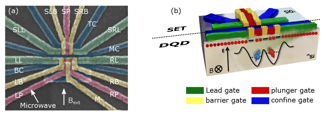
Spin qubits are hosted in a pair of metal-oxide-semiconductor (MOS) dots with isotopically enriched silicon. By using the high vacuum activation annealing technique, we improve the mobility of Si-MOS devices by a factor of two, reaching 1.5 /(V·s) [61]. In this work, we use a DQD that has a similar structure (Ref. [38]) and was fabricated in our lab’s clean room. As shown in Figure 1a, the aluminum electrodes are vaporized on top of the silicon oxide by electron beam evaporation techniques. Between every two layers of the electrodes, an insulating layer of aluminum oxide is formed by thermal oxidation. Figure 1b shows that the electrons are confined in the potential wells and the DQD is formed by applying voltages to the electrodes [62]. In the quantum well, a single electron can tunnel between the two QDs by biasing the electrodes’ voltages. The entire structure consists of a DQD and a single-electron transistor (SET) sensing the charge states in DQD.

Figure 1.
(a) Scanning electron micrograph image of a typical Si-MOS DQD. An SET, which is used as a charge sensor, is confined by the top confine gate (TC), middle confine gate (MC), left barrier gate (SLB), and right barrier gate (SRB) and is tuned by the plunger gate (SP). A DQD is composed of a left lead gate (LL), right lead gate (RL), left barrier gate (LB), middle gate (M), right barrier gate (RB), left plunger gate (LP), and right plunger gate (RP) and is confined by a bottom confine gate (BC) and middle confine gate (MC). We tune the left and right QD via the LP and RP, respectively. The tunneling rate of the QDs can be tuned by the LB and RB. The spin of electrons in the left QD is controlled by applying a microwave pulse to the LP. The right white arrow indicates the direction of an in-plane external magnetic field. (b) Cross-sectional view of a 3D model of the device. Electrodes for different functions are distinguished by different colors. The SET and DQD are on each side of the dotted line. The electrons in the DQD are located under the plunger gates.
2.2. Measurement Circuits
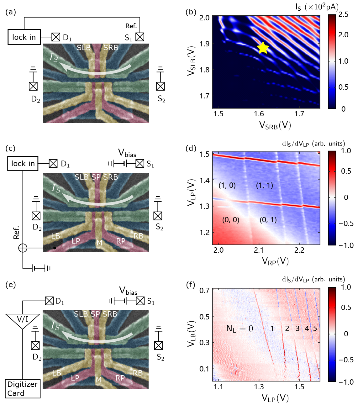
There are three main types of measurement circuits commonly used to characterize the properties of DQDs, as shown in Figure 2a,c,e:

Figure 2.
The three different measurement circuits. The white arrow above the SET indicates the direction of the current (). (a,b) Measurement circuit diagram of the SET using the lock-in amplifier and the Coulomb peak diagram obtained by scanning the voltage of the SET barrier gates (SRB and SLB). The yellow star identifies a sensitive SET position. (c,d) Measurement circuit diagram of the DQD and the charge stability diagram of the DQD obtained by scanning the RP and LP. (e,f) Measurement circuit diagram for measuring the DQD using a current-voltage amplifier and the corresponding charge stability diagram of the left QD.
- Figure 2a: Transport measurements based on a lock-in amplifier. The AC excitation is added to the SET source () by connecting the lock-in amplifier to an external 1000:1 voltage divider, and finally reaches at approximately 50 V, with a lock-in frequency generally between 70 and 1000 Hz. In addition, the drain () is connected back to the lock-in amplifier to demodulate the signal and obtain the currents.
- Figure 2c: Charge detection based on the lock-in amplifier. The bias voltage at is connected to a Stanford Research Systems Isolated Voltage Source (SIM 928) through a 1000:1 voltage divider, reaching at around 500 V, while the AC excitation of the lock-in amplifier (output at approximately 0.5 to 1.5 mV) is connected to LP through an analog summing amplifier (SIM 980, bandwidth of approximately 1 MHz).
- Figure 2e: Charge detection based on a current-voltage amplifier. The source-drain bias is the same as Figure 2c, except no excitation is applied to the LP and is connected to a current-voltage amplifier; here, we use a Femto DLPCA200, connected to a voltage amplifier (SIM 910), an analog filter (SIM 965), and finally to a voltmeter (Agilent 34410) for signal measurement or to a PCI-based waveform digitizer (ATS 460), oscilloscope, etc. for the real-time observation of electron tunneling.
3. Results
3.1. Basic Properties of Silicon QDs
3.1.1. Charge Stability Diagram
Obtaining the QD charge stability diagram by the charge detection method is one of the most basic QD characterization methods [42,43,44]. As shown in Figure 2a–d, according to the method of measuring QDs using the modulation signal of the lock-in amplifier introduced in Section 2, the source () and drain () of the DQD are grounded. We set the voltages of the SLB and SRB near a Coulomb peak so that the SET works sensitively at this position, which is identified by the yellow star in Figure 2b. Then, a voltage of 2.60 V is applied to the LL and RL to ensure that the channel of DQD is turned on. After that, we measured the charge stability diagrams with different gate voltages to obtain the DQD electron occupation numbers and tunneling properties of the left QD. Figure 2d shows the charge stability diagram of the last few electrons in the DQD. The numbers in this figure indicate the electron occupation on the left and right QD. The slope is relatively symmetric with respect to the two electrodes. This indicates that two QDs are formed under electrodes LP and RP. When scanning the voltage of LB and LP, there are continuous electron tunneling lines observed, which correspond to the left QD. As shown in Figure 2f, the tunneling line of the last few electrons in the left QD becomes more invisible when the voltage of LB decreases. This is because a decrease in the LB voltage reduces the tunneling rate of the left QD to the reservoir of .
3.1.2. Detection of Orbital Excited States in Silicon QDs
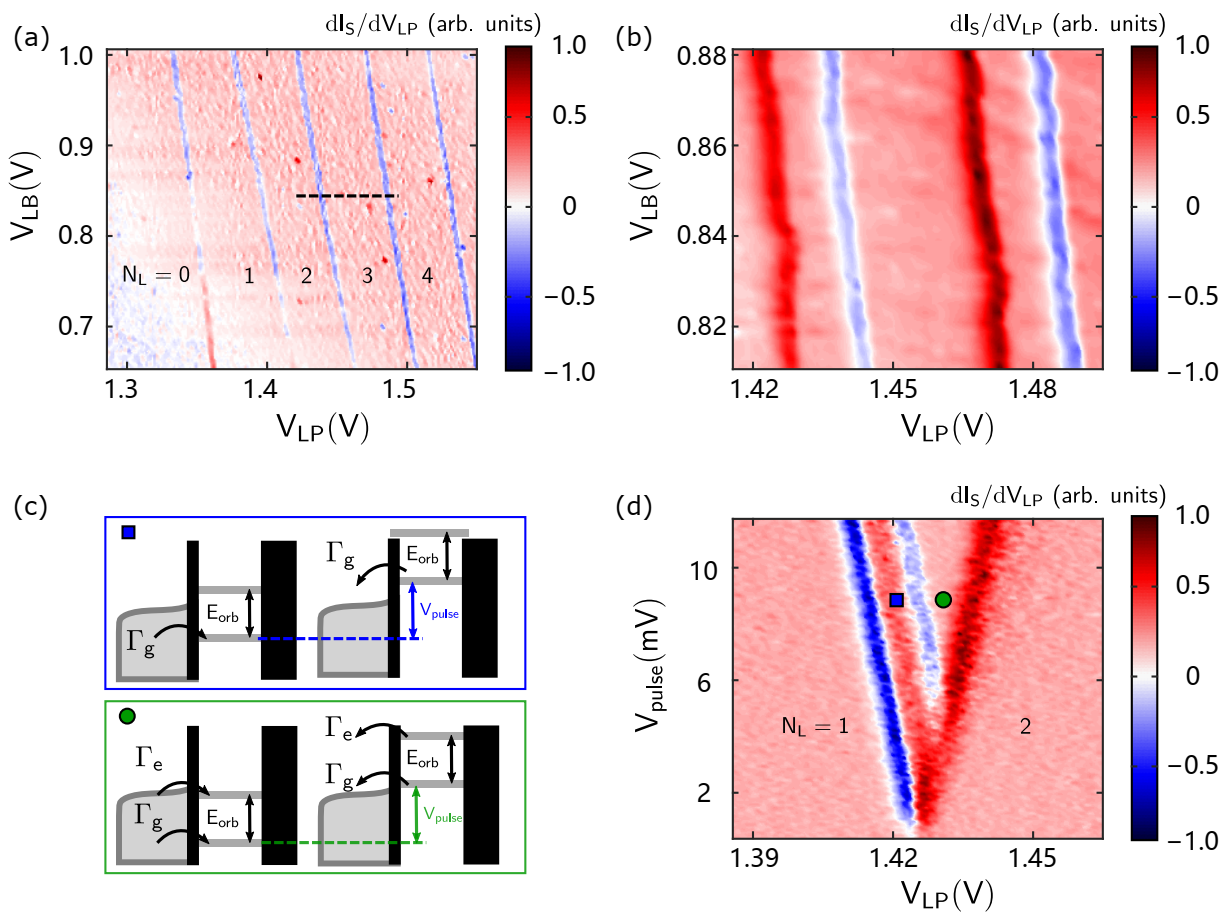
The orbital excited state in silicon QDs is several meV above the ground state, and it can be detected by the pulsed-voltage spectroscopy method [39,63]. Based on the measurement circuit in Figure 2c, we change the modulation signal output from the lock-in amplifier to a square waveform generated by an external arbitrary waveform generator that is synchronized with the lock-in amplifier. By zooming in and remapping, the single tunneling lines in Figure 3a split into pairs of lines in Figure 3b. As shown in Figure 3c, the principle of the pulsed-voltage spectroscopy method is illustrated. When the voltage of LP is set at the position of the blue square in Figure 3d, the electron can tunnel into the ground state of the QD. As the voltage increases, the energy level of the excited state gradually approaches the amplitude window of the square wave. When the excited state enters the window, the electron can tunnel into the excited state, so that another transport line appears parallel to the left line, identified by the green circle in Figure 3d. According to Figure 3d and the extracted lever arm of LP (, which will be discussed in Section 3.1.3), which is 0.33 meV/mV, the calculated energy of excited state is 1.3 meV.
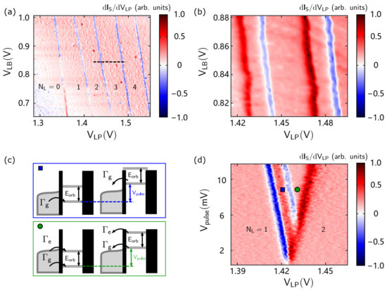
Figure 3.
(a) Charge stability diagram of the QDs obtained by scanning the LB and LP voltages. (b) Zoom in on the QD charge stability diagram after applying a square pulse with a frequency of 687 Hz and an amplitude of 20 mV. (c) Schematic diagram of the square pulse spectrum measurement of the excited orbital state. When the LP voltage increases, the tunneling line of the electron in the excited state appears. (d) Diagram of the excited orbital state obtained by scanning the amplitude of the square pulse and the LP voltage.
3.1.3. Detection of Valley States in Silicon QDs
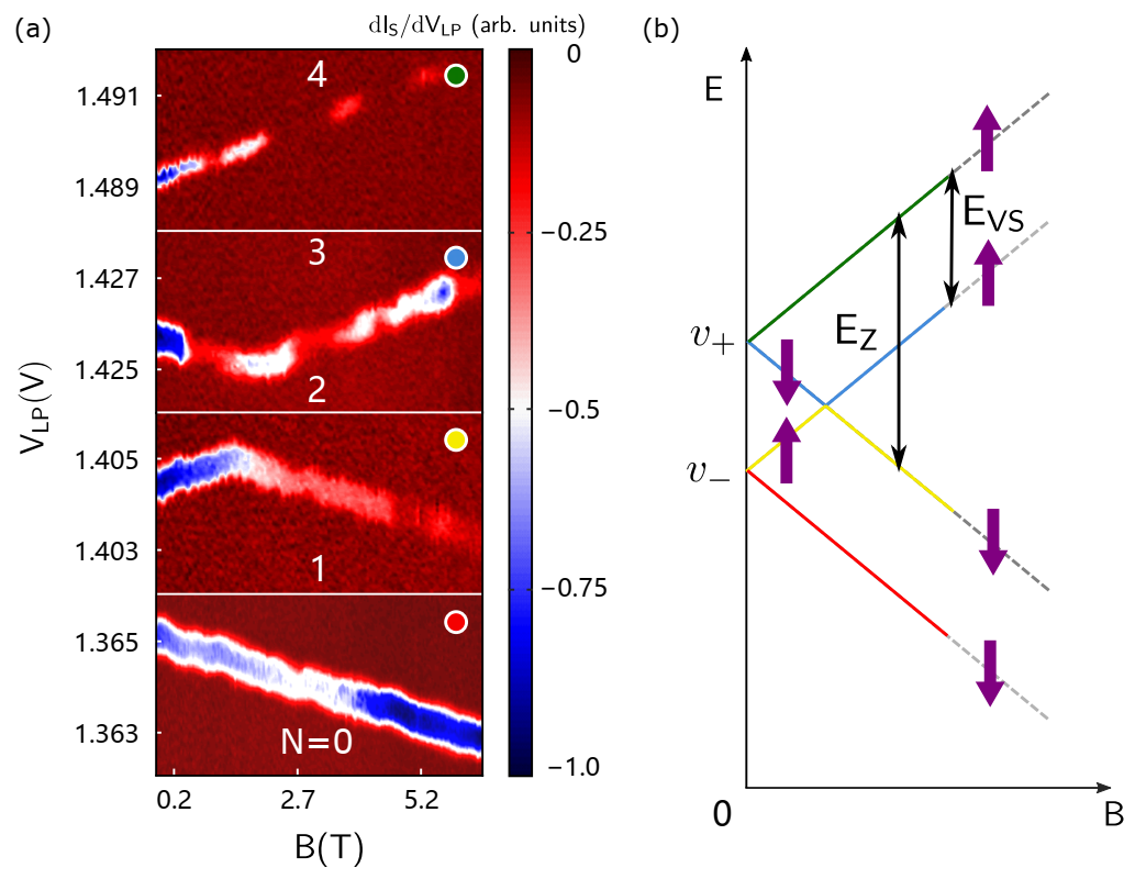
In solid-state physics, due to the six-fold degeneracy at the bottom of the conduction band of silicon, the energy levels at the bottom of the six conduction bands are named as the valley level. In the case of two-dimensional electron gas, the six-fold degeneracy is split into a four-fold degeneration and a double-fold degeneration. Due to the existence of the interfacial electric field, the quadruple degenerate and the double degenerate split further and form valley-level splits [57]. Unlike the orbital state, the splitting energy of the two lowest valley states () in silicon QDs is similar to the Zeemen splitting energy () under the applied magnetic field in our experiment [36,37,38,39,64,65]. Therefore, it is important to determine the splitting energy of the valley state. A commonly used method is to measure the electron tunneling line at different magnetic fields. Here, we tune the energy level of the first four electrons by changing the magnetic field of which the direction of is along the surface of the device and perpendicular to the one-dimensional channel formed by the QD, as shown in Figure 1a. Figure 4a shows the transition lines of the first four electrons in the device in Ref. [38]. The voltage of the first transition line of the QD decreases as the magnetic field increases, while the fourth line increases. Differently, the second transition line increases first and then decreases, and the third line is reversed to the second line.

Figure 4.
The magnetic spectrum and the corresponding diagram of the energy state for different electron numbers in the QDs. (a) The dependence of different electron tunneling lines on the magnetic field, where N = 0, 1, 2, 3, and 4 refer to the number of electrons in the QD. The slopes of the first four electron tunneling lines reveal the lever arms of LP for the first four electrons. (b) Energy state diagram of as a function of the magnetic field. The ordinate is the state energy, and the abscissa is the order of the magnetic field. The purple arrow indicates the direction of the spin. The arrow with represents the energy of the valley splitting.
We use the principle of minimum energy to simply explain this phenomenon, as shown in Figure 4b. When filling the first electron, the electron will be filled to the lowest energy level. As the magnetic field increases, increases, so the energy level of filling the first electron decreases. When filling the second electron, the first electron has been filled to the bottom level. In accordance with the principle of minimum energy, the second electron should be filled with the second-lowest level, but this second-lowest energy level depends on the magnetic field. When the magnetic field is small, the second-lowest energy state is the valley state with spin state up, and vice versa. As shown in Figure 4b, the energy states of the third and fourth electron are mirror-symmetrical to the second and first electrons, respectively. It is obvious from Figure 4b, the position of the kink point is exactly where is equal to , so by using the position of the kink point and the Bohr magneton (), we can obtain:
According to Figure 4a, the of the second electron is 170 eV, and the of the third one is 245 eV. The difference between the of these two electrons is caused by the different LP voltages [38].
Additionally, we can estimate by:
Therefore, the lever arms of the first four electrons are shown in Table 1:

Table 1.
Lever arm for the first four electrons.
3.2. Real-Time Observation of Electron Tunneling in Silicon QDs
The characterization of the orbital state, spin state, and valley state in QDs is based on steady-state measurement. However, to detect more properties of electrons, such as tunneling rate, electron temperature, noise spectrum, spin state, etc., we also need the ability to observe the tunneling process of electrons in QDs in real time [45,46,47,48]. The measurement circuit of real-time detection has been introduced in Section 2, as shown in Figure 2e. Next, we introduce the measurement results of tunneling rate, electron temperature, noise spectrum, and spin state, respectively.
3.2.1. RTS and the Measurement of Electron Temperature
When we align the electrochemical potential of the first electron in the QD with the Fermi surface of the electron reservoir, the electrons will continuously tunnel in and out of the QD (see the green circle in Figure 5a,b). At this time, on the oscilloscope or digitizer, we can see the signal as shown in the inset of Figure 5b. Since tunneling events happen randomly, we call the observed signal a RTS.
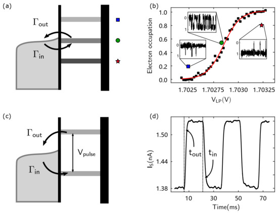
Figure 5.
Measurement of the electron temperature and tunneling rate. (a) Schematic diagram of different positions of the QD energy state and the Fermi surface of the electron reservoir. (b) The probability of electron occupation probability. The electron temperature can be fitted as 223.8 ± 0.8 mK. The inset shows RTS for different electron occupation situations: the circle, square and star marks correspond to the alignment, negative bias and positive bias, respectively. (c) Electron tunnel in the QD when the voltage is high and vice versa. (d) The average current of the electron tunneling by applying a square wave with a 30 ms period. The average current decays exponentially with the tunnel time, and is characteristic of a Poisson process. A single exponential fitting can be used to obtain and .
Ideally, electrons tunnel only when the electrochemical potential in the QD is aligned with the Fermi surface of the electron reservoir. However, in practice, due to the limited electron temperature, the Fermi surface of the electron reservoir will have a certain broadening. Therefore, changes in the electron tunneling events can be observed when the LP voltage is changed. The insets in Figure 5b show that when the electrode voltage increases, the electrochemical potential in the QD decreases, so the probability of the electrons occupying the energy state in the QDs gradually increases and vice versa. By fitting the Fermi distribution to the electron occupancy, we can extract the electron temperature. The specific form of the Fermi distribution function we used here is the following [48]:
where represents the Boltzmann constant, has been calculated in Table 1, and T are fitting parameters. By fitting this equation, the electron temperature of approximately 224 mK is obtained.
3.2.2. Measurement of the Tunneling Rate
For the RTS, we can mark the time of electron tunneling from the reservoir to the QDs as , and the time of electron tunneling from the QDs to the reservoir as . By counting the distribution of and over a long period of time, we can actually determine the time of electron tunneling in and out of the reservoir [45].
Here, we introduce another method based on RTS. As shown in Figure 5c, by applying a square waveform on the LP, the signal will also switch between low and high levels with an approximate square wave period. Figure 5d illustrates that the rising and falling edges of the signal are slower, unlike the square wave from the AWG. Excluding the bandwidth limitation of the SET, the width of the edges represents the electron tunneling times and . By fitting the rising and falling edges exponentially, we can obtain the exact tunneling time values: ms and ms.
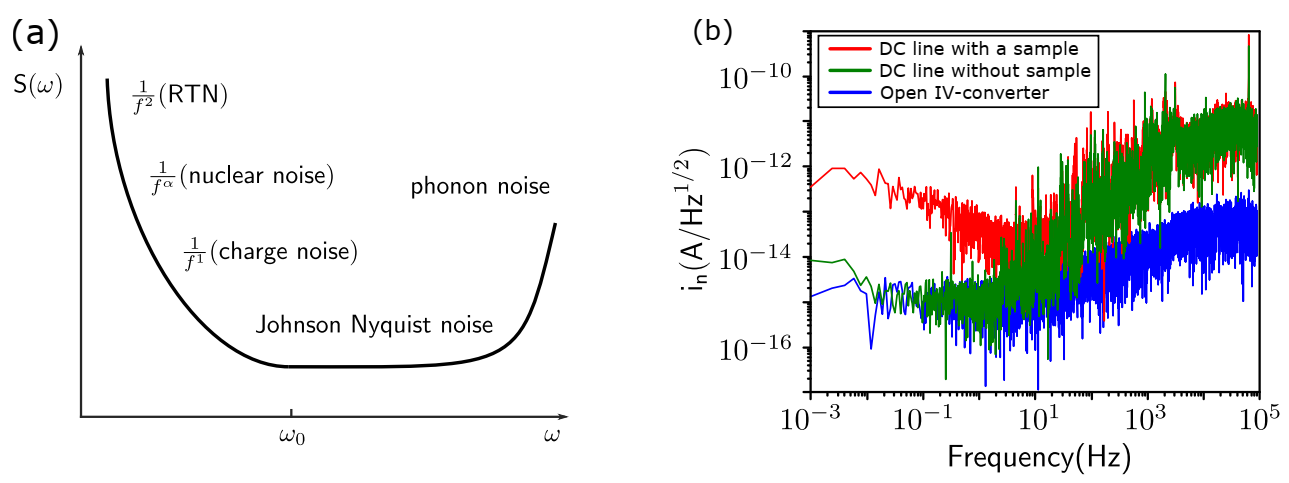
3.2.3. Noise Spectrum
When observing the real-time electron tunneling signal, there will inevitably be noise interference. Analyzing the noise spectrum can help us analyze the source of the noise and then suppress the noise. Figure 6a shows a typical noise spectrum of a QD system but does not include the noise introduced by the measurement system. The QD system suffers from charge noise [29], random telegraph noise (RTN) [40] and nuclear noise [66] at low frequencies. Johnson Nyquist noise and phonon noise are relatively large at high frequencies and affect the spin relaxation time.

Figure 6.
Measurement of the noise spectrum in silicon QD. (a) Typical noise spectrum of a silicon QD; the noise from the measurement system is not included. Here, is the spin resonance frequency. (b) The noise spectrum is measured by a dynamic signal analyzer (SR785) in our system and the spectrum contains three conditions: DC line with a sample, DC line without sample and open I–V converter.
Figure 6b shows the noise spectrum under the different device conditions given in Ref. [38]. The red line is the noise spectrum when the QD is connected. This noise conforms to the law of 1/f. In fact, this is typical charge noise from the QD. The green line is the noise spectrum when the QD is not connected and almost overlaps with the red line above 10 Hz, indicating that the noise above 10 Hz does not come from the QD. The blue line is the noise spectrum when the amplifier input is open, indicating that the noise above 10 Hz comes from the DC line. Compared with Ref. [41], the noise from the QD is low enough for the measurement of the qubit. On the other hand, the capacitance and resistance of the DC line is the main reason for this high-frequency noise. To further reduce the noise source, we can switch to a coaxial line with a smaller capacitance in the future.
3.3. Spin State Readout
After being able to detect the QD charge state and control and measure the tunneling of electrons through a simple square waveform, we now introduce two of the most commonly used methods for spin-to-charge conversion: the Elzerman readout [49,50] and PSB readout [14,51,52,53].
3.3.1. Elzerman Readout
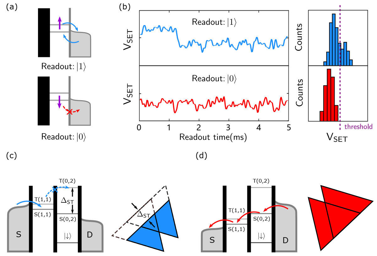
The process of the Elzerman readout is shown in Figure 7a. We set the voltage to locate the Fermi surface of the electron reservoir between the energy state of the electrons with different spin states. Therefore, the spin-up electrons can tunnel to the electron reservoir (after a period of time to load spin down electrons from the electron reservoir), while the spin down electrons cannot. Since the signal of SET responds to the two events of electron tunneling in and out of the QD, a square wave is formed in the signal of the SET. By observing the change in the current, it can be determined whether electron tunneling occurs; then, it can be determined whether the spin state of the electron is up.

Figure 7.
Spin-charge conversion. (a) Schematic diagram to read the spin state by the Elzerman readout. The spin-up electrons can tunnel out because the energy is higher than the Fermi surface of the electron reservoir and vice versa. (b) The measurement result of the spin state is read out by the Elzerman method in our experiment. When the electron in spin-up state tunnels out, there is a high level in the signal. The electron in spin-down state cannot tunnel out, so the signal remains at a low level. (c) Schematic diagram of the energy state and corresponding measurement results of the electron transition current with a negative bias. is the energy difference between the S and T states. When the energy detuning is less than , PSB occurs. (d) Schematic diagram of the energy state with a positive bias. Here, no PSB occurs.
Figure 7b shows a series of the measured SET current signal while reading the spin state. The signal in the top panel has a square pulse, which corresponds to a spin up state. The signal in the bottom panel does not have such a pulse and indicates a spin down state. Based on the above process, we have achieved a single-shot readout of the electron spin state.
3.3.2. PSB
For the PSB readout, we first need to know the double spin eigenstates; the singlet (S) and triplet (T, include , and ) states:
When there is no magnetic field, the singlet state is the ground state. The three-spin triplet state energies degenerate, which is referred to as the T state. This T state is an excited state. Now, we consider two charge states in a DQD: (1,1) and (0,2). For the (0,2) state, there are two electrons in one QD. According to the Pauli exclusion principle, the spin wave function of the electrons in the T state is symmetric, so two electrons must occupy different orbital states. Therefore, S(0,2) and T(0,2) are non-degenerate, as shown in Figure 7c,d. is the energy difference between S(0,2) and T(0,2). However, for the (1,1) state, two electrons are located in their respective QDs, thus avoiding the Pauli exclusion principle and two electrons can occupy one orbital state. Therefore, S(1,1) and T(1,1) are almost degenerate, as shown in Figure 7c,d.
Based on these energy states, we now introduce the PSB readout. As shown in Figure 7c, when a negative bias is applied (the Fermi surface of the source is higher than the drain), electrons in the source can first tunnel to the S(1,1) or T(1,1) state. When tunneling to the S(1,1) state, the electron can continue to tunnel to S(0,2) and then reach the drain to form current. When tunneling to the T(1,1) state, the electron cannot continue to tunnel to S(0,2) due to the PSB, and T(0,2) is higher than T(1,1), so the electron cannot enter any (0,2) charge states, and the current is suppressed. Figure 7d shows the positive bias condition. The Fermi surface of the source is lower than the drain. The electrons in the drain tunnel to the S(0,2) state, and then through the S(1,1) state to the source to form a current. No blockade occurs in the process, so there is current in the entire bias triangle region. In addition, for the PSB readout, we can use the SET to sense the charge states in DQD, and the operating temperature can be raised to higher than 1 kelvin [34,35].
3.3.3. Measurement of Spin Lifetime
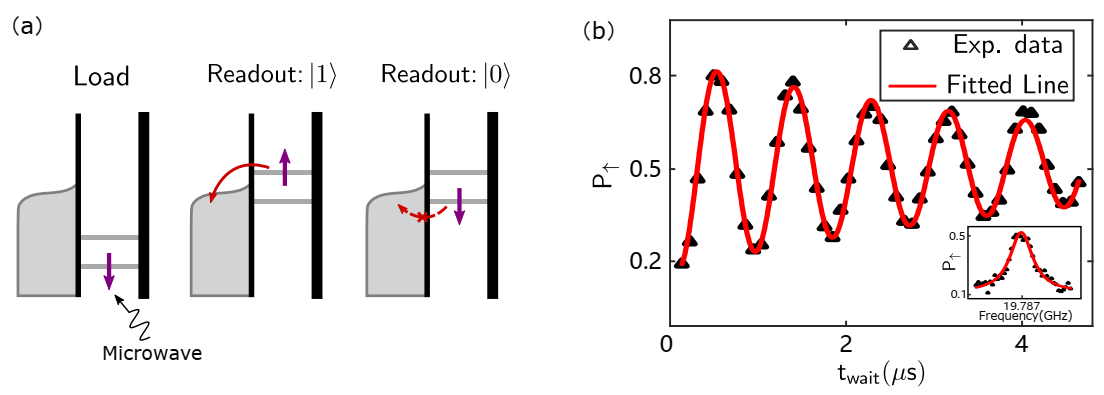
After being able to perform a single-shot measurement to read the spin state, we can use the same waveform to measure the spin lifetime () [50]. The process of a typical single-shot readout is shown in Figure 8a. First, we reduce the voltage for electron evacuating from the QD; this is also referred to as “empty”. Then, we raise the voltage so that electrons can tunnel from the electron reservoir to the QDs, which is also called “load”. At this time the spin state of the electron in QD is random. Finally, we carefully reduce the voltage to locate the Fermi surface of the electron reservoir between the energy state of different spin electrons to “read” the spin state. We count the number of spin relaxation events for different load time periods. Figure 8b illustrates that the probability of the spin up state () decreases exponentially, so the can be obtained by fitting the exponential function.
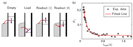
Figure 8.
Schematic diagram and measurement result of . (a) Schematic diagram of a single-shot readout for measurement. (b) Measured spin up probability () as a function of waiting time (). The fitting result of is ms for the left QD.
3.4. Manipulation of the Spin Qubit
Now that we are able to read the spin state via the single-shot readout method, we introduce the manipulation of the spin qubit. There are two mainstream manipulation methods: ESR [16,53,54] and EDSR [23,52,55,56,67,68]. The ESR can be achieved by applying an alternating magnetic field (5–50 T) perpendicular to the external magnetic field (typically 150–1500 mT) via an antenna structure. For EDSR, we apply an alternating electric field combined with spin-orbit coupling to flip the spin. However, the natural spin–orbit coupling in silicon is weak, so we need micromagnets to introduce a gradient magnetic field to construct synthetic spin-orbit coupling. The advantages of EDSR include a fast spin flip rate, low heating, ease of fabrication, etc. However, the additional magnetic field from the micromagnets makes it difficult to find the resonance frequency of the qubit. Therefore, we introduce rapid adiabatic passage to solve this problem.
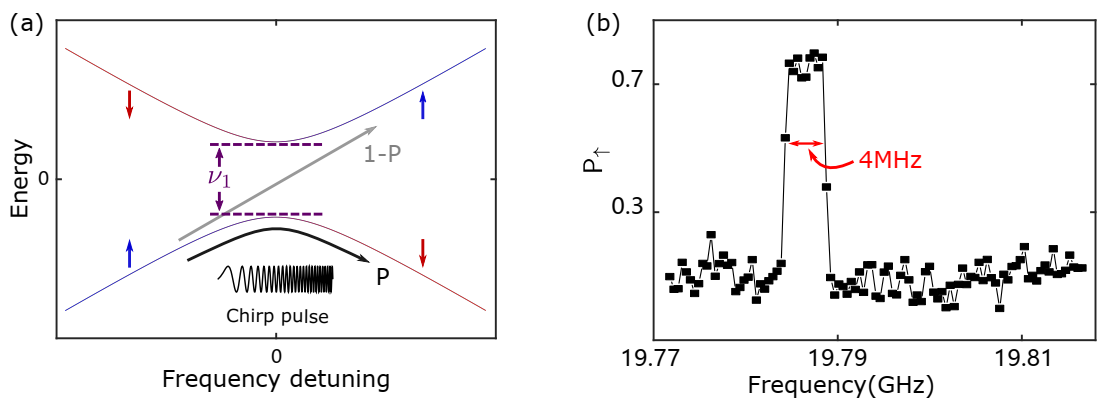
3.4.1. Rapid Adiabatic Passage
We use frequency chirped microwave bursts, and when the excitation frequency passes through the resonance frequency, the electron spin is inverted (see Figure 9b) [23,55,56]. Figure 9a shows the principle of the rapid adiabatic passage process. In the reference frame rotating at the resonance frequency, the Hamiltonian of the system is the following [56]:
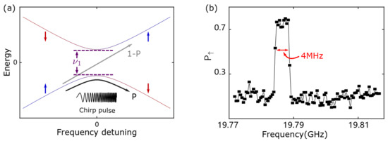
Figure 9.
Schematic explanation and measurement result of rapid adiabatic passage. (a) Schematic explanation of rapid adiabatic passage in the rotating reference frame. (b) as a function of microwave frequency with a 0.5 ms burst time and a 4 MHz frequency modulation depth.
Here, is the microwave frequency detuning from the resonance frequency, and is the spin flip rate.
We use the Landau–Zener theory to solve this time evolution of a two-level system that is described by a linearly time-dependent Hamiltonian. The probability of adiabatic transition from one eigenstate to the other is given by [56]
An electron spin in the state will flip to the state if the microwave frequency sweeps across the resonance frequency. To satisfy the adiabatic evolution condition, the sweep rate cannot be too fast compared with .
3.4.2. Rabi Oscillation
After calibrating the resonant frequency through the rapid adiabatic passage, we now use a single-frequency microwave combined with a single-shot readout to manipulate the qubit [54,56], as shown in the inset of Figure 10b. Figure 10a shows the Rabi pulsing scheme. First, we increase the voltage so that electrons in the or state cannot tunnel from the QDs to the electron reservoir. We apply the microwave pulse before the next stage to flip the electron spin. Then, as mentioned in Section 3.3.3, we carefully decrease the voltage to locate the Fermi surface of the electron reservoir between the energy states of different spin electrons to “read” the spin state. At the end of the “read” phase, the electron spin state will be no matter the spin state at the beginning. Figure 10b shows the result of a Rabi oscillation. As the microwave duration time increases, the spin of the qubit continuously flips between and states. The amplitude of oscillation decreases with time due to noise. We fit the Rabi oscillation with the function . Here, MHz represents the spin flip rate, and s represents the influence of the noise in Figure 10b.

Figure 10.
Schematic diagram and measurement result of Rabi oscillation. (a) Schematic diagram for Rabi oscillation. (b) as a function of . The inset shows as a function of microwave frequency around the resonance frequency GHz.
4. Conclusions
In this paper, we provide an operation guide of Si-MOS QDs for spin qubits. First, we introduce the structure of the devices and the measurement circuit. Next, we show the charge stability diagram and detect the orbital and valley states. Then, we use a digitizer to detect the RTS and measure electron temperature and tunneling rate. Moreover, we introduce two commonly used methods, the Elzerman readout and the PSB readout, and use the single-shot readout method to measure the . Finally, we give a brief introduction of ESR and EDSR, use rapid adiabatic passage to calibrate the resonance frequency of the spin qubit, and show the result of the Rabi oscillation. For future directions, researchers may be interested in hybrid qubits coupling [33], hot qubits [34,35], cryogenic control [69,70], foundry-fabrication [71,72], high fidelity readouts [73,74], and qubit number expansion [75].
Author Contributions
R.-Z.H., R.-L.M., M.N., X.Z. and H.-O.L. performed the experiments. R.-L.M. and M.N. fabricated the sample. G.C., K.W. and Y.Z. helped analyze the data. Z.-Z.K., G.L. and G.-L.W. prepared the silicon wafer. H.-O.L., R.-Z.H., X.Z., R.-L.M., M.N. and G.-P.G. designed the experiment, provided theoretical support, and analyzed the results. H.-O.L. and G.-P.G. supervised the project. R.-Z.H. and H.-O.L. wrote the manuscript, with input from all authors. All authors have read and agreed to the published version of the manuscript.
Funding
This work was supported by National Key Research and Development Program of China (Grant No. 2016YFA0301700), the National Natural Science Foundation of China (Grants No. 12074368, 61922074, 12034018, 11625419 and 62004185), the Anhui initiative in Quantum Information Technologies (Grant No. AHY080000). G.-L.W. acknowledges financial support by Youth Innovation Promotion Association of CAS (Grant No. 2020037). This work was partially carried out at the USTC Center for Micro and Nanoscale Research and Fabrication.
Data Availability Statement
The data presented in this study are available on request from the corresponding authors.
Conflicts of Interest
The authors declare no conflict of interest.
References
- Feynman, R.P. Simulating physics with computers. Int. J. Theor. Phys. 1982, 21, 467–488. [Google Scholar] [CrossRef]
- Shor, P.W. Algorithms for quantum computation: Discrete logarithms and factoring. In Proceedings of the 35th Annual Symposium on Foundations of Computer Science, Santa Fe, NM, USA, 20–22 November 1994; pp. 124–134. [Google Scholar]
- Grover, L.K. A fast quantum mechanical algorithm for database search. In Proceedings of the Twenty-Eighth Annual ACM Symposium on Theory of Computing, Philadelphia, PA, USA, 22–24 May 1996; pp. 212–219. [Google Scholar]
- Loss, D.; DiVincenzo, D.P. Quantum computation with quantum dots. Phys. Rev. 1998, 57, 120–126. [Google Scholar] [CrossRef] [Green Version]
- Di Vincenzo, D.P. The physical implementation of quantum computation. Fortschritte Phys. 2000, 48, 771–783. [Google Scholar] [CrossRef] [Green Version]
- Cirac, J.I.; Zoller, P. Quantum computations with cold trapped ions. Phys. Rev. Lett. 1995, 74, 4091–4094. [Google Scholar] [CrossRef]
- Monroe, C.; Kim, J. Scaling the ion trap quantum processor. Science 2013, 339, 1164–1169. [Google Scholar] [CrossRef] [Green Version]
- Vandersypen, L.M.K.; Steffen, M.; Breyta, G.; Yannoni, C.S.; Sherwood, M.H.; Chuang, I.L. Experimental realization of shor’s quantum factoring algorithm using nuclear magnetic resonance. Nature 2001, 414, 883–887. [Google Scholar] [CrossRef] [Green Version]
- Vandersypen, L.M.K.; Chuang, I.L. NMR techniques for quantum control and computation. Rev. Mod. Phys. 2005, 76, 1037–1069. [Google Scholar] [CrossRef] [Green Version]
- Mooij, J.E.; Orlando, T.P.; Levitov, L.; Tian, L.; Wal, C.H.V.; Lloyd, S. Josephson persistent-current qubit. Science 1999, 285, 1036–1039. [Google Scholar] [CrossRef] [Green Version]
- Krantz, P.; Kjaergaard, M.; Yan, F.; Orlando, T.P.; Gustavsson, S.; Oliver, W.D. A quantum engineer’s guide to superconducting qubits. Appl. Phys. Rev. 2019, 6, 021318. [Google Scholar] [CrossRef]
- Dutt, M.V.G.; Childress, L.; Jiang, L.; Togan, E.; Maze, J.; Jelezko, F.; Zibrov, A.S.; Hemmer, P.R.; Lukin, M.D. Quantum register based on individual electronic and nuclear spin qubits in diamond. Science 2007, 316, 1312–1316. [Google Scholar] [CrossRef] [Green Version]
- Childress, L.; Hanson, R. Diamond NV centers for quantum computing and quantum networks. MRS Bull. 2013, 38, 134–138. [Google Scholar] [CrossRef] [Green Version]
- Petta, J.R.; Johnson, A.C.; Taylor, J.M.; Laird, E.A.; Yacoby, A.; Lukin, M.D.; Marcus, C.M.; Hanson, M.P.; Gossard, A.C. Coherent manipulation of coupled electron spins in semiconductor quantum dots. Science 2005, 309, 2180–2184. [Google Scholar] [CrossRef] [Green Version]
- Elzerman, J.M.; Hanson, R.; Beveren, L.H.W.V.; Tarucha, S.; Vandersypen, L.M.K.; Kouwenhoven, L.P. Semiconductor Few-Electron Quantum Dots as Spin Qubits; Springer: New York, NY, USA, 2005. [Google Scholar]
- Veldhorst, M.; Hwang, J.C.C.; Yang, C.H.; Leenstra, A.W.; de Ronde, B.; Dehollain, J.P.; Muhonen, J.T.; Hudson, F.E.; Itoh, K.M.; Morello, A.; et al. An addressable quantum dot qubit with fault-tolerant control-fidelity. Nat. Nanotechnol. 2014, 9, 981–985. [Google Scholar] [CrossRef] [Green Version]
- Veldhorst, M.; Yang, C.H.; Hwang, J.C.C.; Huang, W.; Dehollain, J.P.; Muhonen, J.T.; Simmons, S.; Laucht, A.; Hudson, F.E.; Itoh, K.M.; et al. A two-qubit logic gate in silicon. Nature 2015, 526, 410–414. [Google Scholar] [CrossRef]
- Kandel, Y.P.; Qiao, H.; Fallahi, S.; Gardner, G.C.; Manfra, M.J.; Nichol, J.M. Adiabatic quantum state transfer in a semiconductor quantum-dot spin chain. Nat. Commun. 2021, 12, 2156. [Google Scholar] [CrossRef]
- Vandersypen, L.M.K.; Bluhm, H.; Clarke, J.S.; Dzurak, A.S.; Ishihara, R.; Morello, A.; Reilly, D.J.; Schreiber, L.R.; Veldhorst, M. Interfacing spin qubits in quantum dots and donors—Hot, dense, and coherent. Npj Quantum Inf. 2017, 3, 34. [Google Scholar] [CrossRef]
- Li, R.; Petit, L.; Franke, D.P.; Dehollain, J.P.; Helsen, J.; Steudtner, M.; Thomas, N.K.; Yoscovits, Z.R.; Singh, K.J.; Wehner, S.; et al. A crossbar network for silicon quantum dot qubits. Sci. Adv. 2018, 4, eaar3960. [Google Scholar] [CrossRef] [PubMed] [Green Version]
- Zwerver, A.M.J.; Krähenmann, T.; Watson, T.F.; Lampert, L.; George, H.C.; Pillarisetty, R.; Bojarski, S.A.; Amin, P.; Amitonov, S.V.; Boter, J.M.; et al. Qubits made by advanced semiconductor manufacturing. arXiv 2021, arXiv:2101.12650. [Google Scholar]
- Maune, B.M.; Borselli, M.G.; Huang, B.; Ladd, T.D.; Deelman, P.W.; Holabird, K.S.; Kiselev, A.A.; Alvarado-Rodriguez, I.; Ross, R.S.; Schmitz, A.E.; et al. Coherent singlet-triplet oscillations in a silicon-based double quantum dot. Nature 2012, 481, 344–347. [Google Scholar] [CrossRef] [PubMed]
- Kawakami, E.; Scarlino, P.; Ward, D.R.; Braakman, F.R.; Savage, D.E.; Lagally, M.G.; Friesen, M.; Coppersmith, S.N.; Eriksson, M.A.; Vandersypen, L.M.K. Electrical control of a long-lived spin qubit in a Si/SiGe quantum dot. Nat. Nanotechnol. 2014, 9, 666–670. [Google Scholar] [CrossRef]
- Watson, T.F.; Philips, S.G.J.; Kawakami, E.; Ward, D.R.; Scarlino, P.; Veldhorst, M.; Savage, D.E.; Lagally, M.G.; Friesen, M.; Coppersmith, S.N.; et al. A programmable two-qubit quantum processor in silicon. Nature 2018, 555, 633–637. [Google Scholar] [CrossRef] [Green Version]
- Zajac, D.M.; Sigillito, A.J.; Russ, M.; Borjans, F.; Taylor, J.M.; Burkard, G.; Petta, J.R. Resonantly driven cnot gate for electron spins. Science 2018, 359, 439–442. [Google Scholar] [CrossRef] [Green Version]
- Huang, W.; Yang, C.H.; Chan, K.W.; Tanttu, T.; Hensen, B.; Leon, R.C.C.; Fogarty, M.A.; Hwang, J.C.C.; Hudson, F.E.; Itoh, K.M.; et al. Fidelity benchmarks for two-qubit gates in silicon. Nature 2019, 569, 532–536. [Google Scholar] [CrossRef] [PubMed]
- Xue, X.; Watson, T.F.; Helsen, J.; Ward, D.R.; Savage, D.E.; Lagally, M.G.; Coppersmith, S.N.; Eriksson, M.A.; Wehner, S.; Vandersypen, L.M.K. Benchmarking gate fidelities in a Si/SiGe two-qubit device. Phys. Rev. 2019, 9, 021011. [Google Scholar] [CrossRef] [Green Version]
- Chan, K.W.; Huang, W.; Yang, C.H.; Hwang, J.C.C.; Hensen, B.; Tanttu, T.; Hudson, F.E.; Itoh, K.M.; Laucht, A.; Morello, A.; et al. Assessment of a silicon quantum dot spin qubit environment via noise spectroscopy. Phys. Rev. Appl. 2018, 10, 044017. [Google Scholar] [CrossRef] [Green Version]
- Yoneda, J.; Takeda, K.; Otsuka, T.; Nakajima, T.; Delbecq, M.R.; Allison, G.; Honda, T.; Kodera, T.; Oda, S.; Hoshi, Y.; et al. A quantum-dot spin qubit with coherence limited by charge noise and fidelity higher than 99.9%. Nat. Nanotechnol. 2018, 13, 102–106. [Google Scholar] [CrossRef] [PubMed]
- Xue, X.; Russ, M.; Samkharadze, N.; Undseth, B.; Sammak, A.; Scappucci, G.; Vandersypen, L.M.K. Computing with spin qubits at the surface code error threshold. arXiv 2021, arXiv:2107.00628. [Google Scholar]
- Mi, X.; Benito, M.; Putz, S.; Zajac, D.M.; Taylor, J.M.; Burkard, G.; Petta, J.R. A coherent spin–photon interface in silicon. Nature 2018, 555, 599. [Google Scholar] [CrossRef] [PubMed] [Green Version]
- Samkharadze, N.; Zheng, G.; Kalhor, N.; Brousse, D.; Sammak, A.; Mendes, U.C.; Blais, A.; Scappucci, G.; Vandersypen, L.M.K. Strong spin-photon coupling in silicon. Science 2018, 359, 1123–1127. [Google Scholar] [CrossRef] [Green Version]
- Borjans, F.; Croot, X.G.; Mi, X.; Gullans, M.J.; Petta, J.R. Resonant microwave-mediated interactions between distant electron spins. Nature 2020, 577, 195–198. [Google Scholar] [CrossRef] [Green Version]
- Petit, L.; Eenink, H.G.J.; Russ, M.; Lawrie, W.I.L.; Hendrickx, N.W.; Philips, S.G.J.; Clarke, J.S.; Vandersypen, L.M.K.; Veldhorst, M. Universal quantum logic in hot silicon qubits. Nature 2020, 580, 355–359. [Google Scholar] [CrossRef] [Green Version]
- Yang, C.H.; Leon, R.C.C.; Hwang, J.C.C.; Saraiva, A.; Tanttu, T.; Huang, W.; Lemyre, J.C.; Chan, K.W.; Tan, K.Y.; Hudson, F.E.; et al. Operation of a silicon quantum processor unit cell above one kelvin. Nature 2020, 580, 350–354. [Google Scholar] [CrossRef] [Green Version]
- Lim, W.H.; Yang, C.H.; Zwanenburg, F.A.; Dzurak, A.S. Spin filling of valley–orbit states in a silicon quantum dot. Nanotechnology 2011, 22, 335704. [Google Scholar] [CrossRef]
- Zajac, D.M.; Hazard, T.M.; Mi, X.; Wang, K.; Petta, J.R. A reconfigurable gate architecture for Si/SiGe quantum dots. Appl. Phys. Lett. 2015, 106, 223507. [Google Scholar] [CrossRef] [Green Version]
- Zhang, X.; Hu, R.; Li, H.; Jing, F.; Zhou, Y.; Ma, R.; Ni, M.; Luo, G.; Cao, G.; Wang, G.; et al. Giant anisotropy of spin relaxation and spin-valley mixing in a silicon quantum dot. Phys. Rev. Lett. 2020, 124, 57701. [Google Scholar] [CrossRef]
- Yang, C.H.; Lim, W.H.; Lai, N.S.; Rossi, A.; Morello, A.; Dzurak, A.S. Orbital and valley state spectra of a few-electron silicon quantum dot. Phys. Rev. 2012, 86, 115319. [Google Scholar] [CrossRef] [Green Version]
- Kamioka, J.; Kodera, T.; Takeda, K.; Obata, T.; Tarucha, S.; Oda, S. Charge noise analysis of metal oxide semiconductor dual-gate Si/SiGe quantum point contacts. J. Appl. Phys. 2014, 115, 203709. [Google Scholar] [CrossRef]
- Freeman, B.M.; Schoenfield, J.S.; Jiang, H. Comparison of low frequency charge noise in identically patterned Si/SiO2 and Si/SiGe quantum dots. Appl. Phys. Lett. 2016, 108, 253108. [Google Scholar] [CrossRef]
- Elzerman, J.M.; Hanson, R.; Greidanus, J.S.; van Beveren, L.H.W.; Franceschi, S.D.; Vandersypen, L.M.K.; Tarucha, S.; Kouwenhoven, L.P. Few-electron quantum dot circuit with integrated charge read out. Phys. Rev. 2003, 67, 161308. [Google Scholar] [CrossRef] [Green Version]
- Borselli, M.G.; Eng, K.; Ross, R.S.; Hazard, T.M.; Holabird, K.S.; Huang, B.; Kiselev, A.A.; Deelman, P.W.; Warren, L.D.; Milosavljevic, I.; et al. Undoped accumulation-mode Si/SiGe quantum dots. Nanotechnology 2015, 26, 375202. [Google Scholar] [CrossRef]
- Lawrie, W.I.L.; Eenink, H.G.J.; Hendrickx, N.W.; Boter, J.M.; Petit, L.; Amitonov, S.V.; Lodari, M.; Wuetz, B.P.; Volk, C.; Philips, S.G.J.; et al. Quantum dot arrays in silicon and germanium. Appl. Phys. Lett. 2020, 116, 080501. [Google Scholar] [CrossRef] [Green Version]
- Vandersypen, L.M.K.; Elzerman, J.M.; Schouten, R.N.; Beveren, L.H.W.V.; Hanson, R.; Kouwenhoven, L.P. Real-time detection of single-electron tunneling using a quantum point contact. Appl. Phys. Lett. 2004, 85, 4394–4396. [Google Scholar] [CrossRef] [Green Version]
- Li, H.; Xiao, M.; Cao, G.; Zhou, C.; Shang, R.; Tu, T.; Guo, G.; Jiang, H.; Guo, G. Back-action-induced non-equilibrium effect in electron charge counting statistics. Appl. Phys. Lett. 2012, 100, 092112. [Google Scholar] [CrossRef]
- House, M.G.; Xiao, M.; Guo, G.; Li, H.; Cao, G.; Rosenthal, M.M.; Jiang, H. Detection and measurement of spin-dependent dynamics in random telegraph signals. Phys. Rev. Lett. 2013, 111, 126803. [Google Scholar] [CrossRef] [Green Version]
- Zajac, D.M.; Hazard, T.M.; Mi, X.; Nielsen, E.; Petta, J.R. Scalable gate architecture for a one-dimensional array of semiconductor spin qubits. Phys. Rev. Appl. 2016, 6, 054013. [Google Scholar] [CrossRef] [Green Version]
- Elzerman, J.M.; Hanson, R.; van Beveren, L.H.W.; Witkamp, B.; Vandersypen, L.M.K.; Kouwenhoven, L.P. Single-shot read-out of an individual electron spin in a quantum dot. Nature 2004, 430, 431–435. [Google Scholar] [CrossRef] [Green Version]
- Morello, A.; Pla, J.J.; Zwanenburg, F.A.; Chan, K.W.; Tan, K.Y.; Huebl, H.; Möttönen, M.; Nugroho, C.D.; Yang, C.; van Donkelaar, J.A.; et al. Single-shot readout of an electron spin in silicon. Nature 2010, 467, 687. [Google Scholar] [CrossRef] [Green Version]
- Johnson, A.C.; Petta, J.R.; Marcus, C.M.; Hanson, M.P.; Gossard, A.C. Singlet-triplet spin blockade and charge sensing in a few-electron double quantum dot. Phys. Rev. 2005, 72, 165308. [Google Scholar] [CrossRef] [Green Version]
- Zhang, X.; Zhou, Y.; Hu, R.; Ma, R.; Ni, M.; Wang, K.; Luo, G.; Cao, G.; Wang, G.; Huang, P.; et al. Controlling synthetic spin-orbit coupling in a silicon quantum dot with magnetic field. Phys. Rev. Appl. 2021, 15, 044042. [Google Scholar] [CrossRef]
- Koppens, F.H.; Buizert, C.; Tielrooij, K.J.; Vink, I.T.; Nowack, K.C.; Meunier, T.; Kouwenhoven, L.P.; Vandersypen, L.M. Driven coherent oscillations of a single electron spin in a quantum dot. Nature 2006, 442, 766–771. [Google Scholar] [CrossRef]
- Pla, J.J.; Tan, K.Y.; Dehollain, J.P.; Lim, W.H.; Morton, J.J.L.; Jamieson, D.N.; Dzurak, A.S.; Morello, A. A single-atom electron spin qubit in silicon. Nature 2012, 489, 541–545. [Google Scholar] [CrossRef] [PubMed]
- Shafiei, M.; Nowack, K.C.; Reichl, C.; Wegscheider, W.; Vandersypen, L.M.K. Resolving spin-orbit- and hyperfine-mediated electric dipole spin resonance in a quantum dot. Phys. Rev. Lett. 2013, 110, 107601. [Google Scholar] [CrossRef] [Green Version]
- Laucht, A.; Kalra, R.; Muhonen, J.T.; Dehollain, J.P.; Mohiyaddin, F.A.; Hudson, F.; McCallum, J.C.; Jamieson, D.N.; Dzurak, A.S.; Morello, A. High-fidelity adiabatic inversion of a 31P electron spin qubit in natural silicon. Appl. Phys. Lett. 2014, 104, 092115. [Google Scholar] [CrossRef] [Green Version]
- Zwanenburg, F.A.; Dzurak, A.S.; Morello, A.; Simmons, M.Y.; Hollenberg, L.C.L.; Klimeck, G.; Rogge, S.; Coppersmith, S.N.; Eriksson, M.A. Silicon quantum electronics. Rev. Mod. Phys. 2013, 85, 961–1019. [Google Scholar] [CrossRef]
- Zhang, X.; Li, H.; Cao, G.; Xiao, M.; Guo, G. Semiconductor quantum computation. Natl. Sci. Rev. 2018, 6, 32–54. [Google Scholar] [CrossRef]
- Zhang, X.; Li, H.; Wang, K.; Cao, G.; Xiao, M.; Guo, G. Qubits based on semiconductor quantum dots. Chin. Phys. 2018, 27, 020305. [Google Scholar] [CrossRef]
- Spruijtenburg, P.C.; Amitonov, S.V.; Wiel, W.G.V.; Zwanenburg, F.A. A fabrication guide for planar silicon quantum dot heterostructures. Nanotechnology 2018, 29, 143001. [Google Scholar] [CrossRef] [Green Version]
- Wang, K.; Li, H.; Luo, G.; Zhang, X.; Jing, F.; Hu, R.; Zhou, Y.; Liu, H.; Wang, G.; Cao, G.; et al. Improving mobility of silicon metal-oxide–semiconductor devices for quantum dots by high vacuum activation annealing. EPL (Europhys. Lett.) 2020, 130, 27001. [Google Scholar] [CrossRef]
- Thorbeck, T.; Zimmerman, N.M. Formation of strain-induced quantum dots in gated semiconductor nanostructures. AIP Adv. 2015, 5, 087107. [Google Scholar] [CrossRef] [Green Version]
- Elzerman, J.M.; Hanson, R.; van Beveren, L.H.W.; Vandersypen, L.M.K.; Kouwenhoven, L.P. Excited-state spectroscopy on a nearly closed quantum dot via charge detection. Appl. Phys. Lett. 2004, 84, 4617–4619. [Google Scholar] [CrossRef] [Green Version]
- Tarucha, S.; Austing, D.G.; Honda, T.; Hage, R.J.V.; Kouwenhoven, L.P. Shell filling and spin effects in a few electron quantum dot. Phys. Rev. Lett. 1996, 77, 3613–3616. [Google Scholar] [CrossRef] [Green Version]
- Jiang, L.; Yang, C.H.; Pan, Z.; Rossi, A.; Dzurak, A.S.; Culcer, D. Coulomb interaction and valley-orbit coupling in si quantum dots. Phys. Rev. 2013, 88, 085311. [Google Scholar] [CrossRef] [Green Version]
- Nakajima, T.; Noiri, A.; Kawasaki, K.; Yoneda, J.; Stano, P.; Amaha, S.; Otsuka, T.; Takeda, K.; Delbecq, M.R.; Allison, G.; et al. Coherence of a driven electron spin qubit actively decoupled from quasistatic noise. Phys. Rev. 2020, 10, 011060. [Google Scholar] [CrossRef] [Green Version]
- Nowack, K.C.; Koppens, F.H.; Nazarov, Y.V.; Vandersypen, L.M. Coherent control of a single electron spin with electric fields. Science 2007, 318, 1430–1433. [Google Scholar] [CrossRef] [PubMed] [Green Version]
- Pioro-Ladrière, M.; Obata, T.; Tokura, Y.; Shin, Y.S.; Kubo, T.; Yoshida, K.; Taniyama, T.; Tarucha, S. Electrically driven single-electron spin resonance in a slanting zeeman field. Nat. Phys. 2008, 4, 776–779. [Google Scholar] [CrossRef]
- Pauka, S.J.; Das, K.; Kalra, R.; Moini, A.; Yang, Y.; Trainer, M.; Bousquet, A.; Cantaloube, C.; Dick, N.; Gardner, G.C.; et al. A cryogenic CMOS chip for generating control signals for multiple qubits. Nat. Electron. 2021, 4, 64–70. [Google Scholar] [CrossRef]
- Xue, X.; Patra, B.; van Dijk, J.P.G.; Samkharadze, N.; Subramanian, S.; Corna, A.; Wuetz, B.P.; Jeon, C.; Sheikh, F.; Juarez-Hernandez, E.; et al. CMOS-based cryogenic control of silicon quantum circuits. Nature 2021, 593, 205–210. [Google Scholar] [CrossRef]
- Ansaloni, F.; Chatterjee, A.; Bohuslavskyi, H.; Bertrand, B.; Hutin, L.; Vinet, M.; Kuemmeth, F. Single-electron operations in a foundry-fabricated array of quantum dots. Nat. Commun. 2020, 11, 6399. [Google Scholar] [CrossRef]
- Gilbert, W.; Saraiva, A.; Lim, W.H.; Yang, C.H.; Laucht, A.; Bertrand, B.; Rambal, N.; Hutin, L.; Escott, C.C.; Vinet, M.; et al. Single-electron operation of a silicon-CMOS 2 × 2 quantum dot array with integrated charge sensing. Nano Lett. 2020, 20, 7882–7888. [Google Scholar] [CrossRef] [PubMed]
- Liu, Y.-Y.; Philips, S.G.J.; Orona, L.A.; Samkharadze, N.; McJunkin, T.; MacQuarrie, E.R.; Eriksson, M.A.; Vandersypen, L.M.K.; Yacoby, A. Radio-frequency reflectometry in silicon-based quantum dots. Phys. Rev. Appl. 2021, 16, 014057. [Google Scholar] [CrossRef]
- Ruffino, A.; Yang, T.; Michniewicz, J.; Peng, Y.; Charbon, E.; Gonzalez-Zalba, M.F. Integrated multiplexed microwave readout of silicon quantum dots in a cryogenic cmos chip. arXiv 2021, arXiv:2101.08295. [Google Scholar]
- Takeda, K.; Noiri, A.; Nakajima, T.; Yoneda, J.; Kobayashi, T.; Tarucha, S. Quantum tomography of an entangled three-qubit state in silicon. Nat. Nanotechnol. 2021. [Google Scholar] [CrossRef] [PubMed]


Publisher’s Note: MDPI stays neutral with regard to jurisdictional claims in published maps and institutional affiliations. |
© 2021 by the authors. Licensee MDPI, Basel, Switzerland. This article is an open access article distributed under the terms and conditions of the Creative Commons Attribution (CC BY) license (https://creativecommons.org/licenses/by/4.0/).