
Bottom-Up Fabrication of DNA-Templated Electronic Nanomaterials and Their Characterization


Abstract
:
1. Introduction
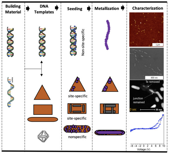
2. Fabrication
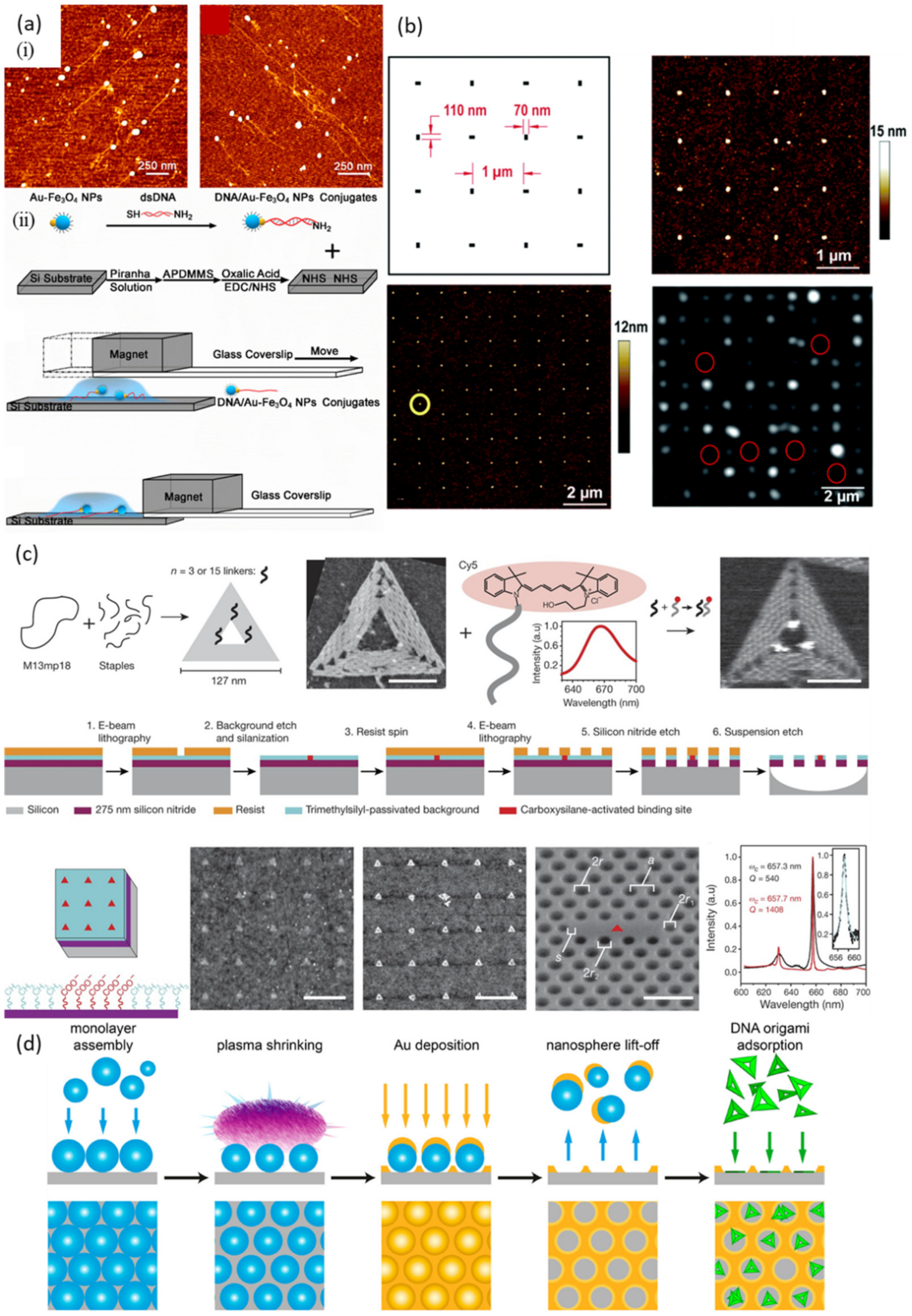
2.1. Substrates
2.2. DNA Templates
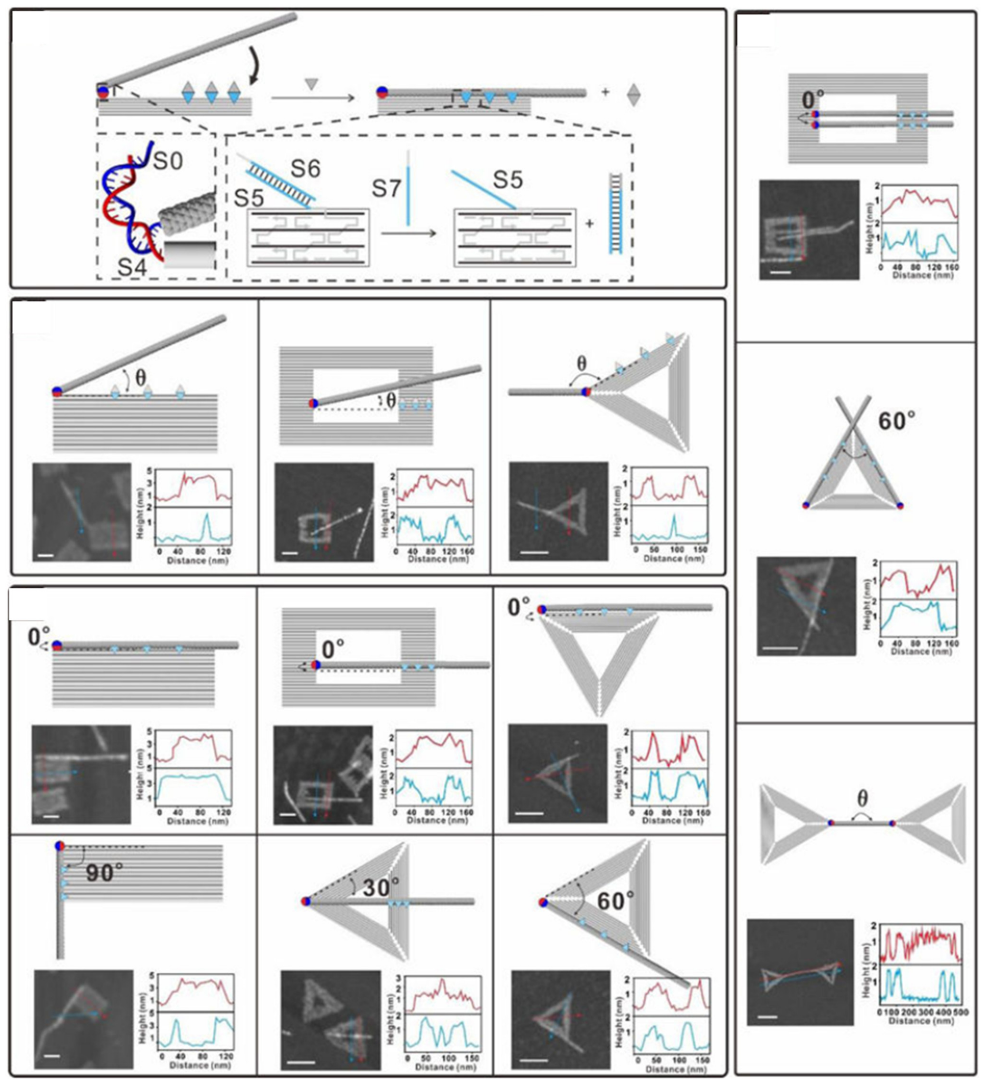
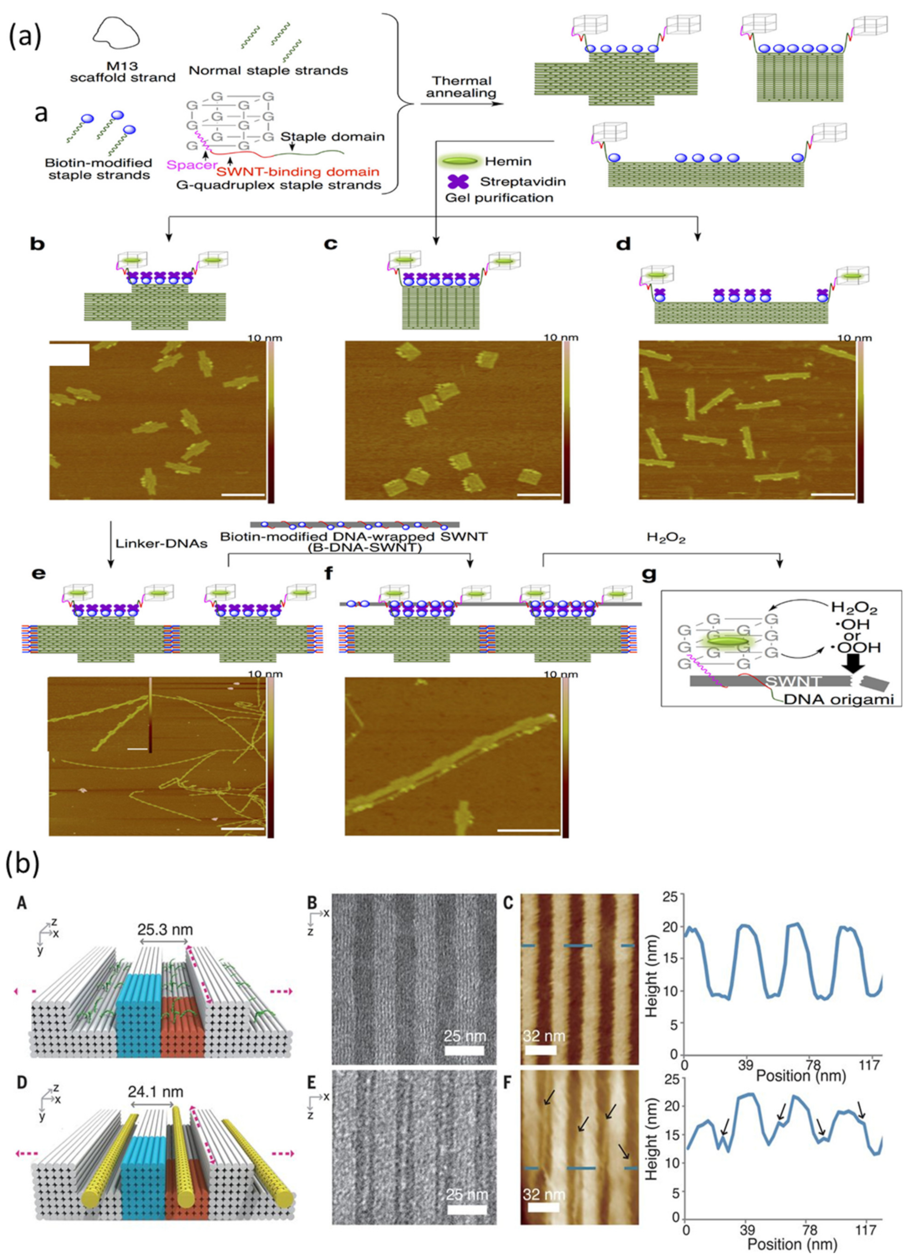
2.2.1. DNA Origami
2.2.2. DNA Origami Stability
2.2.3. DNA Nanotubes
3. Metallization of DNA Templates
3.1. Alignment
3.2. Seeding
3.2.1. Ionic Seeding
3.2.2. Site-Specific Seeding
4. Plating
4.1. Electroless/Chemical Reduction
4.2. Galvanic Displacement
4.3. Photochemical
4.4. Physical Vapor Deposition
5. Non-Metallic Conductors on DNA Nanostructures
5.1. Semiconductors
5.2. Carbon Nanotubes
6. Characterization
6.1. Structural Characterization
6.2. Electrical Characterization
6.3. Photolithography
6.4. Electron Beam Lithography
6.5. Electron Beam Induced Deposition
6.6. Conductive AFM and STM
6.7. Electrochemical Impedance Spectroscopy
7. Conclusions and Outlook
Author Contributions
Funding
Acknowledgments
Conflicts of Interest
Abbreviations
| dsDNA | double-stranded DNA |
| ssDNA | single-stranded DNA |
| NW | nanowire |
| CNT | carbon nanotube |
| 2D | two-dimensional |
| 3D | three-dimensional |
| λ | lambda |
| AFM | atomic force microscopy |
| SEM | scanning electron microscopy |
| TEM | transmission electron microscopy |
| STM | scanning tunneling microscopy |
| EIS | electrochemical impedance spectroscopy |
| NP | nanoparticle |
| NR | nanorod |
| e-beam | electron beam |
| BCP | block co-polymer |
| CTAB | cetyltrimethylammonium bromide |
| FET | field-effect transistor |
| EBL | electron-beam lithography |
| EBID | electron-beam induced deposition |
| I-V | current-voltage |
References
- Madou, M.J. Fundamentals of Microbarication and Nanotechnology, 3rd ed.; CRC Press/Taylor & Francis Group: Boca Raton, FL, USA, 2011; Volume 2, pp. 215–225. [Google Scholar]
- Seeman, N.C. Nucleic Acid Junctions and Lattices. J. Theor. Biol. 1982, 99, 237–247. [Google Scholar] [CrossRef]
- Seeman, N.C.; Sleiman, H.F. DNA nanotechnology. Nat. Rev. Mater. 2017, 3, 17068. [Google Scholar] [CrossRef]
- Peng, Z.; Liu, H. Bottom-up Nanofabrication Using DNA Nanostructures. Chem. Mater. 2016, 28, 1012–1021. [Google Scholar] [CrossRef]
- Lahiri, A.; Pulletikurthi, G.; Endres, F. A Review on the Electroless Deposition of Functional Materials in Ionic Liquids for Batteries and Catalysis. Front Chem. 2019, 7, 85. [Google Scholar] [CrossRef]
- Chen, J.; Seeman, N.C. Synthesis from DNA of a molecule with the connectivity of a cube. Nature 1991, 350, 631–633. [Google Scholar] [CrossRef] [PubMed]
- Alivisatos, A.P.; Johnsson, K.P.; Peng, X.; Wilson, T.E.; Loweth, C.J.; Bruchez, M.P., Jr.; Schultz, P.G. Organization of ‘nanocrystal molecules’ using DNA. Nature 1996, 382, 609–611. [Google Scholar] [CrossRef] [PubMed] [Green Version]
- Mirkin, C.A.; Letsinger, R.L.; Mucic, R.C.; Storhoff, J.L. A DNA-based method for rationally assembling nanoparticles into macroscopic materials. Nature 1996, 382, 607–609. [Google Scholar] [CrossRef]
- Braun, E.; Eichen, Y.; Sivan, U.; Ben-Yoseph, G. DNA-templated assembly and electrode attachment of a conducting silver wire. Nature 1998, 391, 775–778. [Google Scholar] [CrossRef]
- Mbindyo, J.K.N.; Reiss, B.D.; Martin, B.R.; Keating, C.D.; Natan, M.J.; Mallouk, T.E. DNA-Directed Assembly of Gold Nanowires on Complementary Surfaces. Adv. Mater. 2001, 13, 249–254. [Google Scholar] [CrossRef]
- Keren, K.; Berman, R.S.; Buchstab, E.; Sivan, U.; Braun, E. DNA-Templated Carbon Nanotube Field-Effect Transistor. Science 2003, 302, 1380–1382. [Google Scholar] [CrossRef]
- Richter, J.; Mertig, M.; Pompe, W.; Mönch, I.; Schackert, H.K. Construction of highly conductive nanowires on a DNA template. Appl. Phys. Lett. 2001, 78, 536–538. [Google Scholar] [CrossRef] [Green Version]
- Monson, C.F.; Woolley, A.T. DNA-Templated Construction of Copper Nanowires. Nano Lett. 2003, 3, 359–363. [Google Scholar] [CrossRef]
- Seidel, R.; Ciacchi, L.C.; Weigel, M.; Pompe, W.; Mertig, M. Synthesis of Platinum Cluster Chains on DNA Templates: Conditions for a Template-Controlled Cluster Growth. J. Phys. Chem. B 2004, 108, 10801–10811. [Google Scholar] [CrossRef]
- Becerril, H.A.; Ludtke, P.J.; Willardson, B.M.; Woolley, A.T. DNA-Templated Nickel Nanostructures and Protein Assemblies. Langmuir 2006, 22, 10140–10144. [Google Scholar] [CrossRef]
- Gu, Q.; Haynie, D.T. Palladium nanoparticle-controlled growth of magnetic cobalt nanowires on DNA templates. Mater. Lett. 2008, 62, 3047–3050. [Google Scholar] [CrossRef]
- Rothemund, P.W. Folding DNA to create nanoscale shapes and patterns. Nature 2006, 440, 297–302. [Google Scholar] [CrossRef] [Green Version]
- Li, Z.; Liu, M.; Wang, L.; Nangreave, J.; Yan, H.; Liu, Y. Molecular Behavior of DNA Origami in Higher-Order Self-Assembly. J. Am. Chem. Soc. 2010, 132, 13545–13552. [Google Scholar] [CrossRef] [Green Version]
- Douglas, S.M.; Marblestone, A.H.; Teerapittayanon, S.; Vazquez, A.; Church, G.M.; Shih, W.M. Rapid prototyping of 3D DNA-origami shapes with caDNAno. Nucleic Acids Res. 2009, 37, 5001–5006. [Google Scholar] [CrossRef] [Green Version]
- Douglas, S.M.; Dietz, H.; Liedl, T.; Hogberg, B.; Graf, F.; Shih, W.M. Self-assembly of DNA into nanoscale three-dimensional shapes. Nature 2009, 459, 414–418. [Google Scholar] [CrossRef]
- Kershner, R.J.; Bozano, L.D.; Micheel, C.M.; Hung, A.M.; Fornof, A.R.; Cha, J.N.; Rettner, C.T.; Bersani, M.; Frommer, J.; Rothemund, P.W.; et al. Placement and orientation of individual DNA shapes on lithographically patterned surfaces. Nat. Nanotech. 2009, 4, 557–561. [Google Scholar] [CrossRef] [Green Version]
- Gerdon, A.E.; Oh, S.S.; Hsieh, K.; Ke, Y.; Yan, H.; Soh, H.T. Controlled delivery of DNA origami on patterned surfaces. Small 2009, 5, 1942–1946. [Google Scholar] [CrossRef] [PubMed]
- Ding, B.; Wu, H.; Xu, W.; Zhao, Z.; Liu, Y.; Yu, H.; Yan, H. Interconnecting gold islands with DNA origami nanotubes. Nano Lett. 2010, 10, 5065–5069. [Google Scholar] [CrossRef] [Green Version]
- Liu, J.; Geng, Y.; Pound, E.; Gyawali, S.; Ashton, J.R.; Hickey, J.; Woolley, A.T.; Harb, J.N. Metallization of Branched DNA Origami for Nanoelectronic Circuit Fabrication. ACS Nano 2011, 5, 2240–2247. [Google Scholar] [CrossRef]
- Pilo-Pais, M.; Goldberg, S.; Samano, E.; Labean, T.H.; Finkelstein, G. Connecting the nanodots: Programmable nanofabrication of fused metal shapes on DNA templates. Nano Lett. 2011, 11, 3489–3492. [Google Scholar] [CrossRef]
- Sharma, J.C.R.; Andersen, C.S.; Gothelf, K.V.; Yan, H.; Liu, Y. Toward Reliable Gold Nanoparticle Patterning On Self-Assembled DNA Nanoscaffold. J. Am. Chem. Soc. 2008, 130, 7820–7821. [Google Scholar] [CrossRef]
- Pal, S.; Deng, Z.; Ding, B.; Yan, H.; Liu, Y. DNA-origami-directed self-assembly of discrete silver-nanoparticle architectures. Angew. Chem. Int. Ed. 2010, 49, 2700–2704. [Google Scholar] [CrossRef]
- Maune, H.T.; Han, S.P.; Barish, R.D.; Bockrath, M.; Goddard, W.A.I.; Rothemund, P.W.; Winfree, E. Self-assembly of carbon nanotubes into two-dimensional geometries using DNA origami templates. Nat. Nanotechnol. 2010, 5, 61–66. [Google Scholar] [CrossRef] [PubMed] [Green Version]
- Liddle, J.A.; Gallatin, G.M. Lithography, metrology and nanomanufacturing. Nanoscale 2011, 3, 2679–2688. [Google Scholar] [CrossRef]
- Tan, S.J.; Campolongo, M.J.; Luo, D.; Cheng, W. Building plasmonic nanostructures with DNA. Nat. Nanotechnol. 2011, 6, 268–276. [Google Scholar] [CrossRef] [PubMed]
- Pillers, M.A.; Lieberman, M. Thermal stability of DNA origami on mica. J. Vac. Sci. Technol. B 2014, 32, 040602. [Google Scholar] [CrossRef]
- Gopinath, A.; Miyazono, E.; Faraon, A.; Rothemund, P.W. Engineering and mapping nanocavity emission via precision placement of DNA origami. Nature 2016, 535, 401–405. [Google Scholar] [CrossRef]
- Linko, V.; Shen, B.; Tapio, K.; Toppari, J.J.; Kostiainen, M.A.; Tuukkanen, S. One-step large-scale deposition of salt-free DNA origami nanostructures. Sci. Rep. 2015, 5, 15634. [Google Scholar] [CrossRef] [Green Version]
- Katrivas, L.; Kempinski, B.; Kuchuk, K.; Sivan, U.; Kotlyar, A. Multiply Modified Repeating DNA Templates for Production of Novel DNA-Based Nanomaterial. Bioconj. Chem. 2019, 30, 2201–2208. [Google Scholar] [CrossRef]
- Brun, C.; Elchinger, P.-H.; Nonglaton, G.; Tidiane-Diagne, C.; Tiron, R.; Thuaire, A.; Gasparutto, D.; Baillin, X. Metallic Conductive Nanowires Elaborated by PVD Metal Deposition on Suspended DNA Bundles. Small 2017, 13, 1700956. [Google Scholar] [CrossRef] [PubMed]
- Gür, F.N.; Schwarz, F.W.; Ye, J.; Diez, S.; Schmidt, T.L. Toward Self-Assembled Plasmonic Devices: High-Yield Arrangement of Gold Nanoparticles on DNA Origami Templates. ACS Nano 2016, 10, 5374–5382. [Google Scholar] [CrossRef] [PubMed]
- Mathur, D.; Klein, W.P.; Chiriboga, M.; Bui, H.; Oh, E.; Nita, R.; Naciri, J.; Johns, P.; Fontana, J.; Diaz, S.A.; et al. Analyzing fidelity and reproducibility of DNA templated plasmonic nanostructures. Nanoscale 2019, 11, 20693–20706. [Google Scholar] [CrossRef]
- Shen, B.; Linko, V.; Tapio, K.; Kostiainen, M.A.; Toppari, J.J. Custom-shaped metal nanostructures based on DNA origami silhouettes. Nanoscale 2015, 7, 11267–11272. [Google Scholar] [CrossRef] [Green Version]
- Schreiber, R.; Santiago, I.; Ardavan, A.; Turberfield, A.J. Ordering Gold Nanoparticles with DNA Origami Nanoflowers. ACS Nano 2016, 10, 7303–7306. [Google Scholar] [CrossRef]
- Kim, H.; Surwade, S.P.; Powell, A.; O’Donnell, C.; Liu, H. Stability of DNA Origami Nanostructure under Diverse Chemical Environments. Chem. Mater. 2014, 26, 5265–5273. [Google Scholar] [CrossRef]
- Kim, H.; Arbutina, K.; Xu, A.; Liu, H. Increasing the stability of DNA nanostructure templates by atomic layer deposition of Al2O3 and its application in imprinting lithography. Beil. J. Nano. 2017, 8, 2363–2375. [Google Scholar] [CrossRef] [PubMed] [Green Version]
- Owczarzy, R.; You, Y.; Moreira, B.G.; Manthey, J.A.; Huang, L.; Behlke, M.A.; Walder, J.A. Effects of Sodium Ions on DNA Duplex Oligomers: Improved Predictions of Melting Temperatures. Biochemistry 2004, 43, 3537–3554. [Google Scholar] [CrossRef] [PubMed]
- Wei, X.; Nangreave, J.; Jiang, S.; Yan, H.; Liu, Y. Mapping the thermal behavior of DNA origami nanostructures. J. Am. Chem. Soc. 2013, 135, 6165–6176. [Google Scholar] [CrossRef]
- Jungmann, R.; Liedl, T.; Sobey, T.L.; Shih, W.M.; Simmel, F.C. Isothermal Assembly of DNA Origami Structures Using Denaturing Agents. J. Am. Chem. Soc. 2008, 130, 10062–10063. [Google Scholar] [CrossRef] [PubMed]
- Sobey, T.L.; Renner, S.; Simmel, F.C. Assembly and melting of DNA nanotubes from single-sequence tiles. J. Phys. Cond. Matt. 2009, 21, 034112. [Google Scholar] [CrossRef] [PubMed]
- Bashar, S.; Lee, C.-W.; Lee, J.; Kim, B.; Gnapareddy, B.; Shin, J.; Dugasani, S.R.; Park, S.H. Hairpin embedded DNA lattices grown on a mica substrate. RSC Adv. 2013, 3, 19876–19879. [Google Scholar] [CrossRef]
- Xin, Y.; Kielar, C.; Zhu, S.; Sikeler, C.; Xu, X.; Moser, C.; Grundmeier, G.; Liedl, T.; Heuer-Jungemann, A.; Smith, D.M.; et al. Cryopreservation of DNA Origami Nanostructures. Small 2020, 16, e1905959. [Google Scholar] [CrossRef] [Green Version]
- Kielar, C.; Xin, Y.; Shen, B.; Kostiainen, M.A.; Grundmeier, G.; Linko, V.; Keller, A. On the Stability of DNA Origami Nanostructures in Low-Magnesium Buffers. Angew. Chem. Int. Ed. 2018, 57, 9470–9474. [Google Scholar] [CrossRef]
- Kielar, C.; Xin, Y.; Xu, X.; Zhu, S.; Gorin, N.; Grundmeier, G.; Moser, C.; Smith, D.M.; Keller, A. Effect of Staple Age on DNA Origami Nanostructure Assembly and Stability. Molecules 2019, 24, 2577. [Google Scholar] [CrossRef] [Green Version]
- Teschome, B.; Facsko, S.; Gothelf, K.V.; Keller, A. Alignment of Gold Nanoparticle-Decorated DNA Origami Nanotubes: Substrate Prepatterning versus Molecular Combing. Langmuir 2015, 31, 12823–12829. [Google Scholar] [CrossRef]
- Ranasinghe, D.R.; Aryal, B.R.; Westover, T.R.; Jia, S.; Davis, R.C.; Harb, J.N.; Schulman, R.; Woolley, A.T. Seeding, Plating and Electrical Characterization of Gold Nanowires Formed on Self-Assembled DNA Nanotubes. Molecules 2020, 25, 4817. [Google Scholar] [CrossRef]
- Mohammed, A.M.; Šulc, P.; Zenk, J.; Schulman, R. Self-assembling DNA nanotubes to connect molecular landmarks. Nat. Nanotechnol. 2016, 12, 312–316. [Google Scholar] [CrossRef]
- Ganguly, S.; Paul, S.; Yehezkeli, O.; Cha, J.; Caruthers, M.H. Boranephosphonate DNA-Mediated Metallization of Single-Walled Carbon Nanotubes. Chem. Mater. 2017, 29, 2239–2245. [Google Scholar] [CrossRef]
- Hossen, M.M.; Bendickson, L.; Palo, P.E.; Yao, Z.; Nilsen-Hamilton, M.; Hillier, A.C. Creating metamaterial building blocks with directed photochemical metallization of silver onto DNA origami templates. Nanotechnology 2018, 29, 355603. [Google Scholar] [CrossRef] [Green Version]
- Luo, X.; Lachance-Brais, C.; Bantle, A.; Sleiman, H.F. The assemble, grow and lift-off (AGLO) strategy to construct complex gold nanostructures with pre-designed morphologies. Chem. Sci. 2020, 11, 4911–4921. [Google Scholar] [CrossRef] [PubMed] [Green Version]
- Aryal, B.R.; Ranasinghe, D.R.; Westover, T.R.; Calvopiña, D.G.; Davis, R.C.; Harb, J.N.; Woolley, A.T. DNA origami mediated electrically connected metal—semiconductor junctions. Nano Res. 2020, 13, 1419–1426. [Google Scholar] [CrossRef]
- Piskunen, P.; Shen, B.; Julin, S.; Ijas, H.; Toppari, J.J.; Kostiainen, M.A.; Linko, V. DNA Origami-Mediated Substrate Nanopatterning of Inorganic Structures for Sensing Applications. J. Vis. Exp. 2019, 151, e60313. [Google Scholar] [CrossRef] [Green Version]
- Li, N.; Shang, Y.; Xu, R.; Jiang, Q.; Liu, J.; Wang, L.; Cheng, Z.; Ding, B. Precise Organization of Metal and Metal Oxide Nanoclusters into Arbitrary Patterns on DNA Origami. J. Am. Chem. Soc. 2019, 141, 17968–17972. [Google Scholar] [CrossRef] [PubMed]
- Shen, B.; Linko, V.; Tapio, K.; Pikker, S.; Lemma, T.; Gopinath, A.; Gothelf, K.V.; Kostiainen, M.A.; Toppari, J.J. Plasmonic nanostructures through DNA-assisted lithography. Sci. Adv. 2018, 4, eaap8978. [Google Scholar] [CrossRef] [PubMed] [Green Version]
- Aryal, B.R.; Westover, T.R.; Ranasinghe, D.R.; Calvopina, D.G.; Uprety, B.; Harb, J.N.; Davis, R.C.; Woolley, A.T. Four-Point Probe Electrical Measurements on Templated Gold Nanowires Formed on Single DNA Origami Tiles. Langmuir 2018, 34, 15069–15077. [Google Scholar] [CrossRef]
- Zhang, T.; Hartl, C.; Frank, K.; Heuer-Jungemann, A.; Fischer, S.; Nickels, P.C.; Nickel, B.; Liedl, T. 3D DNA Origami Crystals. Adv. Mater. 2018, 30, e1800273. [Google Scholar] [CrossRef]
- Zhan, P.; Wen, T.; Wang, Z.G.; He, Y.; Shi, J.; Wang, T.; Liu, X.; Lu, G.; Ding, B. DNA Origami Directed Assembly of Gold Bowtie Nanoantennas for Single-Molecule Surface-Enhanced Raman Scattering. Angew. Chem. Int. Ed. 2018, 57, 2846–2850. [Google Scholar] [CrossRef]
- Zhan, P.; Dutta, P.K.; Wang, P.; Song, G.; Dai, M.; Zhao, S.X.; Wang, Z.G.; Yin, P.; Zhang, W.; Ding, B.; et al. Reconfigurable Three-Dimensional Gold Nanorod Plasmonic Nanostructures Organized on DNA Origami Tripod. ACS Nano 2017, 11, 1172–1179. [Google Scholar] [CrossRef] [PubMed] [Green Version]
- Teschome, B.; Facsko, S.; Schonherr, T.; Kerbusch, J.; Keller, A.; Erbe, A. Temperature-Dependent Charge Transport through Individually Contacted DNA Origami-Based Au Nanowires. Langmuir 2016, 32, 10159–10165. [Google Scholar] [CrossRef]
- Gates, E.P.; Jensen, J.K.; Harb, J.N.; Woolley, A.T. Optimizing gold nanoparticle seeding density on DNA origami. RSC Adv. 2015, 5, 8134–8141. [Google Scholar] [CrossRef]
- Pearson, A.C.; Liu, J.; Pound, E.; Uprety, B.; Woolley, A.T.; Davis, R.C.; Harb, J.N. DNA origami metallized site specifically to form electrically conductive nanowires. J. Phys. Chem. B 2012, 116, 10551–10560. [Google Scholar] [CrossRef]
- Weichelt, R.; Ye, J.; Banin, U.; Eychmuller, A.; Seidel, R. DNA-Mediated Self-Assembly and Metallization of Semiconductor Nanorods for the Fabrication of Nanoelectronic Interfaces. Chem. Eur. J. 2019, 25, 9012–9016. [Google Scholar] [CrossRef] [PubMed]
- Bayrak, T.; Helmi, S.; Ye, J.; Kauert, D.; Kelling, J.; Schonherr, T.; Weichelt, R.; Erbe, A.; Seidel, R. DNA-Mold Templated Assembly of Conductive Gold Nanowires. Nano Lett. 2018, 18, 2116–2123. [Google Scholar] [CrossRef]
- Brassat, K.; Ramakrishnan, S.; Bürger, J.; Hanke, M.; Doostdar, M.; Lindner, J.K.N.; Grundmeier, G.; Keller, A. On the Adsorption of DNA Origami Nanostructures in Nanohole Arrays. Langmuir 2018, 34, 14757–14765. [Google Scholar] [CrossRef] [PubMed]
- Sun, W.; Shen, J.; Zhao, Z.; Arellano, N.; Rettner, C.; Tang, J.; Cao, T.; Zhou, Z.; Ta, T.; Streit, J.K.; et al. Precise pitch-scaling of carbon nanotube arrays within three-dimensional DNA nanotrenches. Science 2020, 368, 874–877. [Google Scholar] [CrossRef]
- Liu, J.; Wang, X.; Zhang, W. Atomic Force Microscopy Imaging Study of Aligning DNA by Dumbbell-like Au–Fe3O4 Magnetic Nanoparticles. Langmuir 2018, 34, 14875–14881. [Google Scholar] [CrossRef]
- Shaali, M.; Woller, J.G.; Johansson, P.G.; Hannestad, J.K.; de Battice, L.; Aissaoui, N.; Brown, T.; El-Sagheer, A.H.; Kubatkin, S.; Lara-Avila, S.; et al. Site-selective immobilization of functionalized DNA origami on nanopatterned Teflon AF. J. Mater. Chem. C 2017, 5, 7637–7643. [Google Scholar] [CrossRef]
- Shetty, R.M.; Brady, S.R.; Rothemund, P.W.K.; Hariadi, R.F.; Gopinath, A. Low-Cost, Bottom-up fabrication of large-scale single-molecule nanoarrays by DNA origami placement. bioRxiv 2020. [Google Scholar] [CrossRef]
- Pearson, A.C.; Pound, E.; Woolley, A.T.; Linford, M.R.; Harb, J.N.; Davis, R.C. Chemical Alignment of DNA Origami to Block Copolymer Patterned Arrays of 5 nm Gold Nanoparticles. Nano Lett. 2011, 11, 1981–1987. [Google Scholar] [CrossRef] [PubMed]
- Zhang, Y.; Peng, R.; Xu, F.; Ke, Y. Hierarchical Self-Assembly of Cholesterol-DNA Nanorods. Bioconjug. Chem. 2019, 30, 1845–1849. [Google Scholar] [CrossRef]
- Kasyanenko, N.; Qiushi, Z.; Bakulev, V.; Osolodkov, M.; Sokolov, P.; Demidov, V. DNA binding with acetate bis (1, 10-phenanthroline) silver (I) monohydrate in a solution and metallization of formed structures. Polymers 2017, 9, 211. [Google Scholar] [CrossRef] [PubMed] [Green Version]
- Vecchioni, S.; Capece, M.C.; Toomey, E.; Nguyen, L.; Ray, A.; Greenberg, A.; Fujishima, K.; Urbina, J.; Paulino-Lima, I.G.; Pinheiro, V. Construction and characterization of metal ion-containing DNA nanowires for synthetic biology and nanotechnology. Sci. Rep. 2019, 9, 6942. [Google Scholar] [CrossRef] [PubMed]
- González-Olvera, J.C.; Mercader-Trejo, F.; Ramos-López, E.; Rodríguez-López, A.; Álvarez-López, A.; Flores-Juárez, C.R.; Herrera-Basurto, R. Crystallization of metallic nanoparticles on short DNA oligonucleotides in alkaline aqueous solution. J. Nanopart. Res. 2020, 22, 63. [Google Scholar] [CrossRef]
- Kasyanenko, N.A.; Andreeva, A.A.; Baryshev, A.V.; Bakulev, V.M.; Likhodeeva, M.N.; Vorontsov-Velyaminov, P.N. DNA Integration with Silver and Gold Nanoparticles: Enhancement of DNA Optical Anisotropy. J. Phys. Chem. B 2019, 123, 9557–9566. [Google Scholar] [CrossRef]
- Almaky, M.; Hassamien, R.; Clegg, W.; Harrington, R.; Houlton, A.; Horrocks, B. Metal-Conductive Polymer Core-Shell Nanowires: Electroless Reduction of Pd and Cu on Polypyrrole/DNA Templates Bearing 2-2’-Bipyridyl Groups. Int. J. Sci. Res. Sci. Technol. 2020, 7, 406–423. [Google Scholar]
- Dugasani, S.R.; Kim, D.Y.; Gnapareddy, B.; Yoo, S.; Jung, J.H.; Park, S.H. Large-Scale Fabrication of Copper-Ion-Coated Deoxyribonucleic Acid Hybrid Fibers by Ion Exchange and Self-Metallization. ACS Omega 2019, 4, 16462–16470. [Google Scholar] [CrossRef] [PubMed] [Green Version]
- Yoo, S.; Dugasani, S.R.; Chopade, P.; Kesama, M.R.; Gnapareddy, B.; Park, S.H. Metal and Lanthanide Ion-Co-doped Synthetic and Salmon DNA Thin Films. ACS Omega 2019, 4, 6530–6537. [Google Scholar] [CrossRef]
- Mohamed, H.D.A.; Watson, S.M.; Horrocks, B.R.; Houlton, A. Chemical and electrochemical routes to DNA-templated rhodium nanowires. J. Mater. Chem. C 2015, 3, 438–446. [Google Scholar] [CrossRef] [Green Version]
- Yamada, R.; Nomura, I.; Yamaguchi, Y.; Matsuda, Y.; Hattori, Y.; Tada, H.; Ono, A.; Tanaka, Y. Electrical conductance measurement of Hg(II)-mediated DNA duplex in buffered aqueous solution. Nucleos. Nucl. Acids 2020, 39, 1083–1087. [Google Scholar] [CrossRef] [PubMed]
- Ouyang, X.; Wang, M.; Guo, L.; Cui, C.; Liu, T.; Ren, Y.; Zhao, Y.; Ge, Z.; Guo, X.; Xie, G. DNA Nanoribbon-Templated Self-Assembly of Ultrasmall Fluorescent Copper Nanoclusters with Enhanced Luminescence. Angew. Chem. Int. Ed. 2020, 59, 11836–11844. [Google Scholar] [CrossRef] [PubMed]
- Jia, S.; Wang, J.; Xie, M.; Sun, J.; Liu, H.; Zhang, Y.; Chao, J.; Li, J.; Wang, L.; Lin, J. Programming DNA origami patterning with non-canonical DNA-based metallization reactions. Nat. Comm. 2019, 10, 5597. [Google Scholar] [CrossRef] [Green Version]
- Ding, B.Q.; Deng, Z.T.; Yan, H.; Cabrini, S.; Zuckermann, R.N.; Bokor, J. Gold Nanoparticle Self-Similar Chain Structure Organized by DNA Origami. J. Am. Chem. Soc. 2009, 132, 3248–3249. [Google Scholar] [CrossRef]
- Hung, A.M.; Micheel, C.M.; Bozano, L.D.; Osterbur, L.W.; Wallraff, G.M.; Cha, J.N. Large-area spatially ordered arrays of gold nanoparticles directed by lithographically confined DNA origami. Nat. Nanotech. 2010, 5, 121–126. [Google Scholar] [CrossRef]
- Uprety, B.; Gates, E.P.; Geng, Y.; Woolley, A.T.; Harb, J.N. Site-specific metallization of multiple metals on a single DNA origami template. Langmuir 2014, 30, 1134–1141. [Google Scholar] [CrossRef] [PubMed]
- Uprety, B.; Westover, T.; Stoddard, M.; Brinkerhoff, K.; Jensen, J.; Davis, R.C.; Woolley, A.T.; Harb, J.N. Anisotropic Electroless Deposition on DNA Origami Templates to Form Small Diameter Conductive Nanowires. Langmuir 2017, 33, 726–735. [Google Scholar] [CrossRef]
- Uprety, B.; Jensen, J.; Aryal, B.R.; Davis, R.C.; Woolley, A.T.; Harb, J.N. Directional Growth of DNA-Functionalized Nanorods to Enable Continuous, Site-Specific Metallization of DNA Origami Templates. Langmuir 2017, 33, 10143–10152. [Google Scholar] [CrossRef]
- Helmi, S.; Ziegler, C.; Kauert, D.J.; Seidel, R. Shape-controlled synthesis of gold nanostructures using DNA origami molds. Nano Lett. 2014, 14, 6693–6698. [Google Scholar] [CrossRef]
- Ye, J.; Helmi, S.; Teske, J.; Seidel, R. Fabrication of Metal Nanostructures with Programmable Length and Patterns Using a Modular DNA Platform. Nano Lett. 2019, 19, 2707–2714. [Google Scholar] [CrossRef]
- Sun, W.; Boulais, E.; Hakobyan, Y.; Wang, W.L.; Guan, A.; Bathe, M.; Yin, P. Casting inorganic structures with DNA molds. Science 2014, 346, 1258361. [Google Scholar] [CrossRef] [Green Version]
- Shen, L.; Pan, V.; Li, H.; Zhang, Y.; Wang, P.; Ke, Y. Programmable assembly of gold nanoparticle nanoclusters and lattices. J. Mater. Chem. B 2020, 8, 6810–6813. [Google Scholar] [CrossRef] [PubMed]
- Zessin, J.; Fischer, F.; Heerwig, A.; Kick, A.; Boye, S.; Stamm, M.; Kiriy, A.; Mertig, M. Tunable Fluorescence of a Semiconducting Polythiophene Positioned on DNA Origami. Nano Lett. 2017, 17, 5163–5170. [Google Scholar] [CrossRef] [PubMed]
- Mallory, G.O.; Hajdu, J.B. Electroless Plating: Fundamentals and Applications; American Electroplaters and Surface Finishers Society: Orlando, FL, USA, 1990; pp. 2–5. [Google Scholar]
- Stern, A.; Eidelshtein, G.; Zhuravel, R.; Livshits, G.I.; Rotem, D.; Kotlyar, A.; Porath, D. Highly Conductive Thin Uniform Gold-Coated DNA Nanowires. Adv. Mater. 2018, 30, e1800433. [Google Scholar] [CrossRef] [PubMed]
- Liu, J.; Uprety, B.; Gyawali, S.; Woolley, A.T.; Myung, N.V.; Harb, J.N. Fabrication of DNA-templated Te and Bi2Te3 nanowires by galvanic displacement. Langmuir 2013, 29, 11176–11184. [Google Scholar] [CrossRef]
- Ichimura, M.; Gunasekaran, M.; Sueyoshi, T.; Rusop, M.; Soga, T. Photochemical Deposition of Semiconductor Thin Films and Their Application for Solar Cells and Gas Sensors. AIP. Conf. Proc. 2009, 1136, 138–145. [Google Scholar]
- Bouzakis, K.-D.; Michailidis, N. Physical Vapor Deposition (PVD). In CIRP Encyclopedia of Production Engineering; CIRP: Berlin/Heidelberg, Germany, 2018; pp. 1–8. [Google Scholar]
- Vittala, S.K.; Saraswathi, S.K.; Joseph, J. Fullerene Cluster Assisted Self-Assembly of Short DNA Strands into Semiconducting Nanowires. Chem. Eur. J. 2017, 23, 15759–15765. [Google Scholar] [CrossRef]
- Choi, J.; Chen, H.; Li, F.; Yang, L.; Kim, S.S.; Naik, R.R.; Ye, P.D.; Choi, J.H. Nanomanufacturing of 2D Transition Metal Dichalcogenide Materials Using Self-Assembled DNA Nanotubes. Small 2015, 11, 5520–5527. [Google Scholar] [CrossRef]
- Wang, X.; Sha, R.; Kristiansen, M.; Hernandez, C.; Hao, Y.; Mao, C.; Canary, J.W.; Seeman, N.C. An Organic Semiconductor Organized into 3D DNA Arrays by “Bottom-up” Rational Design. Angew. Chem. Int. Ed. 2017, 56, 6445–6448. [Google Scholar] [CrossRef] [PubMed]
- Nurdillayeva, R.; Oshido, A.; Bamford, T.; El-Zubir, O.; Houlton, A.; Hedley, J.; Pike, A.; Horrocks, B. Inkjet printing and electrical characterisation of DNA-templated cadmium sulphide nanowires. Nanotechnology 2018, 29, 135704. [Google Scholar] [CrossRef] [PubMed]
- Han, M.J.; McBride, M.; Risteen, B.; Zhang, G.; Khau, B.V.; Reichmanis, E.; Yoon, D.K. Highly Oriented and Ordered Water-Soluble Semiconducting Polymers in a DNA Matrix. Chem. Mater. 2019, 32, 688–696. [Google Scholar] [CrossRef]
- Wang, X.; Li, C.; Niu, D.; Sha, R.; Seeman, N.C.; Canary, J.W. Construction of a DNA Origami Based Molecular Electro-optical Modulator. Nano Lett. 2018, 18, 2112–2115. [Google Scholar] [CrossRef]
- Al-Mahamad, L.L.; El-Zubir, O.; Smith, D.G.; Horrocks, B.R.; Houlton, A. A coordination polymer for the site-specific integration of semiconducting sequences into DNA-based materials. Nat. Comm. 2017, 8, 720. [Google Scholar] [CrossRef] [Green Version]
- Pei, H.; Sha, R.; Wang, X.; Zheng, M.; Fan, C.; Canary, J.W.; Seeman, N.C. Organizing End-Site-Specific SWCNTs in Specific Loci Using DNA. J. Am. Chem. Soc. 2019, 141, 11923–11928. [Google Scholar] [CrossRef]
- Zhang, Y.; Mao, X.; Li, F.; Li, M.; Jing, X.; Ge, Z.; Wang, L.; Liu, K.; Zhang, H.; Fan, C.; et al. Nanoparticle-Assisted Alignment of Carbon Nanotubes on DNA Origami. Angew. Chem. Int. Ed. 2020, 59, 4892–4896. [Google Scholar] [CrossRef]
- Atsumi, H.; Belcher, A.M. DNA Origami and G-Quadruplex Hybrid Complexes Induce Size Control of Single-Walled Carbon Nanotubes via Biological Activation. ACS Nano 2018, 12, 7986–7995. [Google Scholar] [CrossRef]
- Zhang, Y.; Li, F.; Li, M.; Mao, X.; Jing, X.; Liu, X.; Li, Q.; Li, J.; Wang, L.; Fan, C.; et al. Encoding Carbon Nanotubes with Tubular Nucleic Acids for Information Storage. J. Am. Chem. Soc. 2019, 141, 17861–17866. [Google Scholar] [CrossRef]
- Mirzapoor, A.; Turner, A.P.F.; Tiwari, A.; Ranjbar, B. Electrochemical detection of DNA mismatches using a branch-shaped hierarchical SWNT-DNA nano-hybrid bioelectrode. Mater. Sci. Eng. C 2019, 104, 109886. [Google Scholar] [CrossRef]
- Zhao, M.; Chen, Y.; Wang, K.; Zhang, Z.; Streit, J.K.; Fagan, J.A.; Tang, J.; Zheng, M.; Yang, C.; Zhu, Z.; et al. DNA-directed nanofabrication of high-performance carbon nanotube field-effect transistors. Science 2020, 368, 878–881. [Google Scholar] [CrossRef] [PubMed]
- Binnig, G.; Quate, C.F.; Gerber, C. Atomic force microscope. Phys. Rev. Lett. 1986, 56, 930–933. [Google Scholar] [CrossRef] [PubMed] [Green Version]
- Nixon, W.C. Scanning Electron Microscopy. Microelect. Reliab. 1965, 4, 55–57. [Google Scholar] [CrossRef]
- Yang, J.; Song, Z.; Liu, S.; Zhang, Q.; Zhang, C. Dynamically Arranging Gold Nanoparticles on DNA Origami for Molecular Logic Gates. ACS Appl. Mater. Interf. 2016, 8, 22451–22456. [Google Scholar] [CrossRef] [PubMed]
- Tapio, K.; Toppari, J.J. Characterization of Emergence of the Coulomb Blockade in a Pearl-Like DNA-AuNP Assembly. J. Self Assem. Mol. Elec. 2017, 5, 31–44. [Google Scholar] [CrossRef] [Green Version]
- Utke, I.M.S.; Russel, P. Nanofabrication Using Focused Ion and Electron Beams; Oxford University Press: New York, NY, USA, 2012. [Google Scholar]
- Westover, T.R.; Aryal, B.R.; Ranasinghe, D.R.; Uprety, B.; Harb, J.N.; Woolley, A.T.; Davis, R.C. Impact of Polymer-Constrained Annealing on the Properties of DNA Origami-Templated Gold Nanowires. Langmuir 2020, 36, 6661–6667. [Google Scholar] [CrossRef]
- Giacobbe, S.; Pezzella, C.; Della Ventura, B.; Giacobelli, V.G.; Rossi, M.; Fontanarosa, C.; Amoresano, A.; Sannia, G.; Velotta, R.; Piscitelli, A. Green synthesis of conductive polyaniline by Trametes versicolor laccase using a DNA template. Eng. Life Sci. 2019, 19, 631–642. [Google Scholar] [CrossRef] [Green Version]


| DNA Template | Dimension | Shape | Substrate | Attached Material(s) | Reference |
|---|---|---|---|---|---|
| Single-Stranded | 2D | Linear | NA | CNT | [53] |
| Double-Stranded | 3D | Lattice | NA | Au | [54] |
| 2D | Linear Wire | SiO2 | Al/Au | [35] | |
| DNA Origami | 2D | Sheet (Tile) | Mica/Silica | Au | [55] |
| 2D | Bar | SiO2 | Au/Te | [56] | |
| 2D | Rhombus | Mica | Au | [37] | |
| 2D | Bowtie | SiO2 | Au | [57] | |
| 2D | Triangle | NA | Pd/Fe2O3 | [58] | |
| 2D | Bowtie | SiN/Al2O3 | Au | [59] | |
| 2D | Tile | SiO2 | Au | [54] | |
| 3D | Rhombohedral | NA | Au | [60] | |
| 2D | Bowtie | Si/Glass | Au | [61] | |
| 3D | Tripods | Si | Au | [62] | |
| 2D | Bar | SiO2 | Au | [63] | |
| 3D | Tubular Bundle | NA | Au | [35] | |
| 2D | Planet-Satellites | Solid | Ag-Au/Organic | [36] | |
| 2D | Tubular Bundle | Si | Au | [39] | |
| 2D | Triangle | Si | Au/Ag | [64] | |
| 2D | Toroidal | Si | Au core/Ag shell | [32] | |
| 2D | T Shape | SiO2 | Au | [38] | |
| 2D/3D | Tile/Bowtie/Tube | Si/Glass | Au | [65] | |
| 3D | DNA Molds | Si | Au | [66] | |
| 3D | DNA Molds | Si | Au | [67] | |
| 3D | Long DNA Molds | Si | Au | [68] | |
| 2D | Triangle/Rectangle | Mica | NA | [47] | |
| 2D | Triangle | Si | Au Film | [49] | |
| 2D | Hexagonal Lattices | Mica | Proteins | [69] | |
| 2D | DNA Tube | PMMA/PLLA | CNT | [40] | |
| 3D | DNA Brick | - | CNT | [70] |
| Material | Form of Seed | Seed Size (nm) | Seed Coating | Seeding Technique | Template Geometry | Plating Technique |
Potential Applications | Final Structure Yield | Ref. |
|---|---|---|---|---|---|---|---|---|---|
| Au Te | NP NR | 45 ± 9, 9 ± 2 72 ± 15, 21 ± 3 | DNA CTAB | site-specific | linear | electroless | nanoelectronics | >60% | [56] |
| CdS Au | NR NP | 45 × 5 5 | DNA | site-specific | linear | electroless | nanoelectronics | 70 ± 7% | [67] |
| Fullerene-aniline | NP | 3.2 | Aniline | non-covalent interactions | linear | N/A | nanotechnology | N/A | [102] |
| Au | NP | 12 | DNA | site-specific | linear, triangle, Y and L-shape, square | electroless | nanoelectronics and nanoplasmonics | >80% | [55] |
| Au | Nano-prism | 80 | DNA | site-specific | bowtie | N/A | photonics | 62% | [62] |
| Au | NP | 5 | DNA | site-specific | linear | electroless | nanoelectronics | N/A | [68] |
| Au | NP | 17, 28, 42, 56 | DNA | site-specific | linear | N/A | optoelectronics/nanomedicine | 17% | [36] |
| Au | NP | 5, 10 | DNA | site-specific | tetragonal, hexagonal | N/A | plasmonics | 81–94% | [65] |
| Au | NP | 10 | DNA | site-specific | cluster and honeycomb lattices | N/A | biomedical | N/A | [92] |
| Au | NR | 6 × 25 | CTAB | electrostatic | linear | electroless | nanoelectronics | 57% | [63] |
| Rh | ion | N/A | N/A | electrostatic DNA/Rh ions | linear | electrochemical | nanowires | N/A | [83] |
| Nanowire Material | Method of Contact | Nanowire Size | Resistance (R) or Resistivity (ρ) | Ref. |
|---|---|---|---|---|
| Au | EBL | 13–29 nm × 400 nm | ρ = 8.9 × 10⁻⁷ Ω m | [90] |
| Ni | EBL | 100 nm × 10 µm | ρ = 1.0 × 10⁻⁵ to 4.8 × 10⁻⁴ Ω m | [99] |
| Au | EBL | 30 nm × 412 nm | R = 120 MΩ to 2.8 GΩ | [64] |
| Au | EBL | 10–15 nm | Conductive | [118] |
| Au | EBL | 40 nm × 800 nm | R = 90 Ω | [68] |
| Au | EBID | 10 nm × 130 nm | ρ = 4.24 × 10⁻⁵ Ω m | [60] |
| Doped film | Direct to silver pad | Thin film | R = 2–14 MΩ | [82] |
| Au/Te | EBID | 17 nm × 400 nm | Continuous/semiconducting | [56] |
| Au | EBID | 10–20 nm × 400 nm | R = 150 Ω | [120] |
| Rh | Conductive AFM | <10 nm diameter | ρ = 41–65 Ω cm | [68] |
| PANI | EIS | NA | R = 3.4–3.9 kΩ | [121] |
| Au-thioguanosine | Platinum electrodes | 2 nm | Conductive after doping | [108] |
| Au/Ti | Photolithography | 60–80 nm × 0.8–2 µm | R = 7.7–43 Ω | [35] |
Publisher’s Note: MDPI stays neutral with regard to jurisdictional claims in published maps and institutional affiliations. |
© 2021 by the authors. Licensee MDPI, Basel, Switzerland. This article is an open access article distributed under the terms and conditions of the Creative Commons Attribution (CC BY) license (https://creativecommons.org/licenses/by/4.0/).
Share and Cite
Pang, C.; Aryal, B.R.; Ranasinghe, D.R.; Westover, T.R.; Ehlert, A.E.F.; Harb, J.N.; Davis, R.C.; Woolley, A.T. Bottom-Up Fabrication of DNA-Templated Electronic Nanomaterials and Their Characterization. Nanomaterials 2021, 11, 1655. https://doi.org/10.3390/nano11071655
Pang C, Aryal BR, Ranasinghe DR, Westover TR, Ehlert AEF, Harb JN, Davis RC, Woolley AT. Bottom-Up Fabrication of DNA-Templated Electronic Nanomaterials and Their Characterization. Nanomaterials. 2021; 11(7):1655. https://doi.org/10.3390/nano11071655
Chicago/Turabian StylePang, Chao, Basu R. Aryal, Dulashani R. Ranasinghe, Tyler R. Westover, Asami E. F. Ehlert, John N. Harb, Robert C. Davis, and Adam T. Woolley. 2021. "Bottom-Up Fabrication of DNA-Templated Electronic Nanomaterials and Their Characterization" Nanomaterials 11, no. 7: 1655. https://doi.org/10.3390/nano11071655
APA StylePang, C., Aryal, B. R., Ranasinghe, D. R., Westover, T. R., Ehlert, A. E. F., Harb, J. N., Davis, R. C., & Woolley, A. T. (2021). Bottom-Up Fabrication of DNA-Templated Electronic Nanomaterials and Their Characterization. Nanomaterials, 11(7), 1655. https://doi.org/10.3390/nano11071655