
Bipolar Switching Properties of the Transparent Indium Tin Oxide Thin Film Resistance Random Access Memories


Abstract
1. Introduction
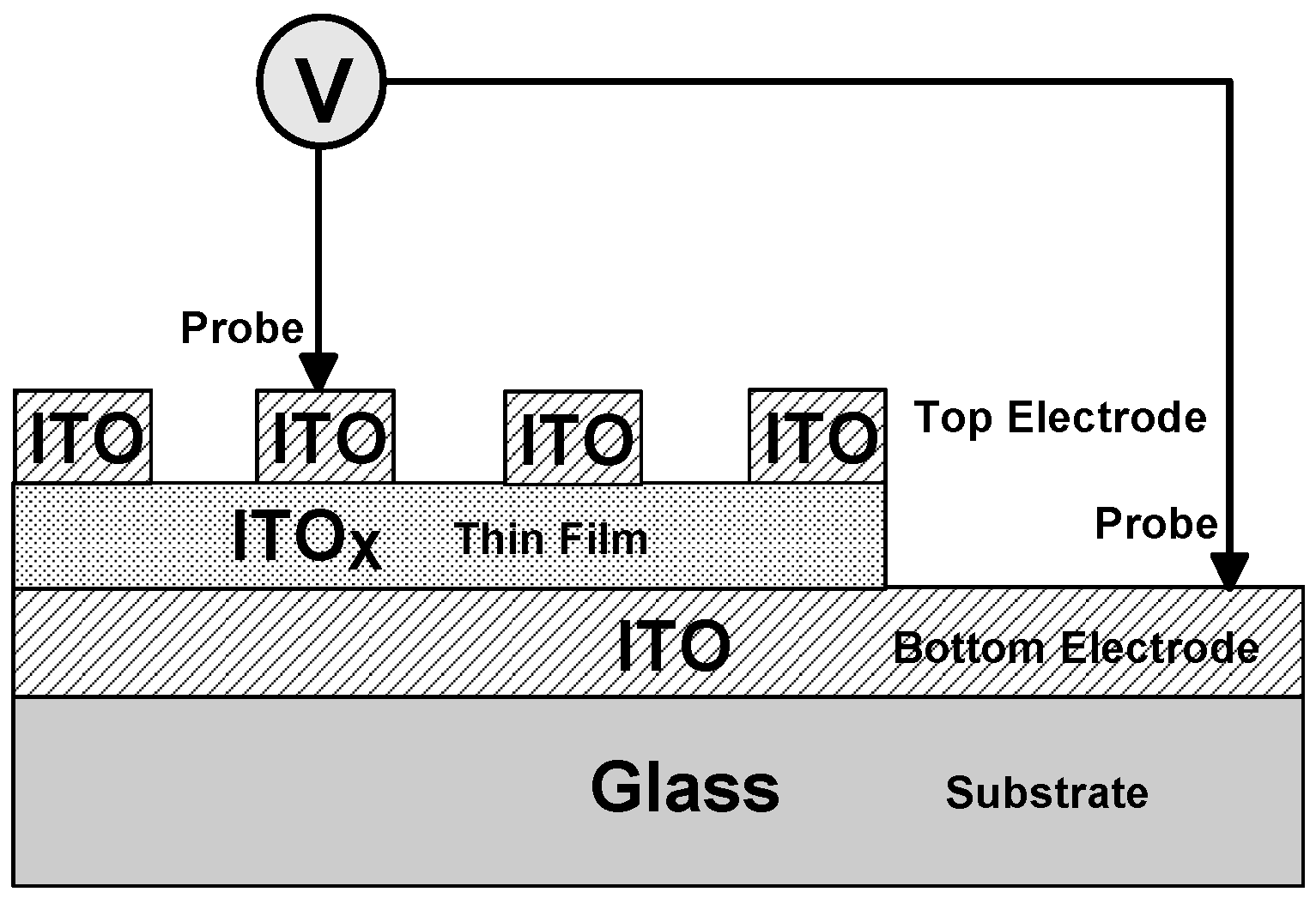
2. Experimental Procedures
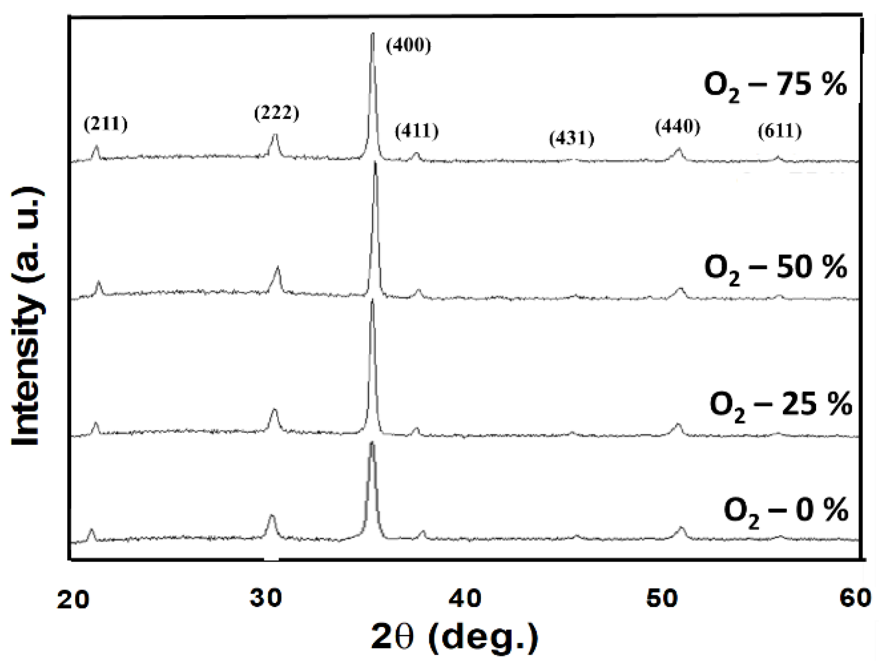
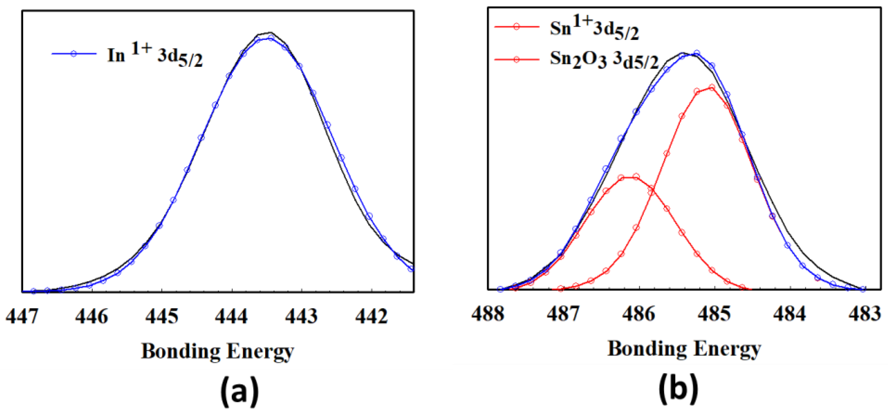
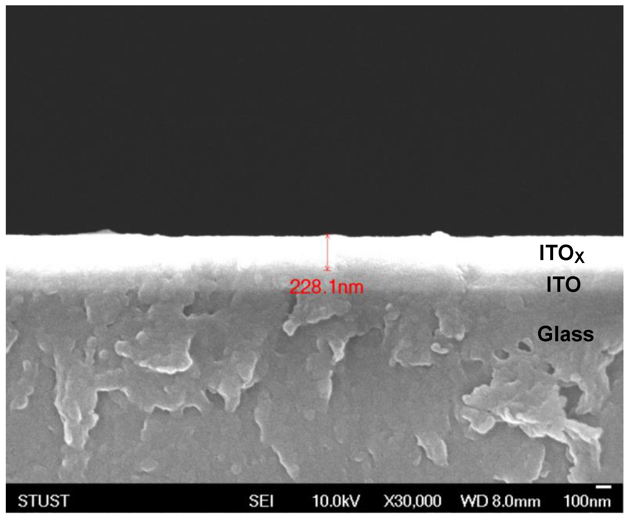
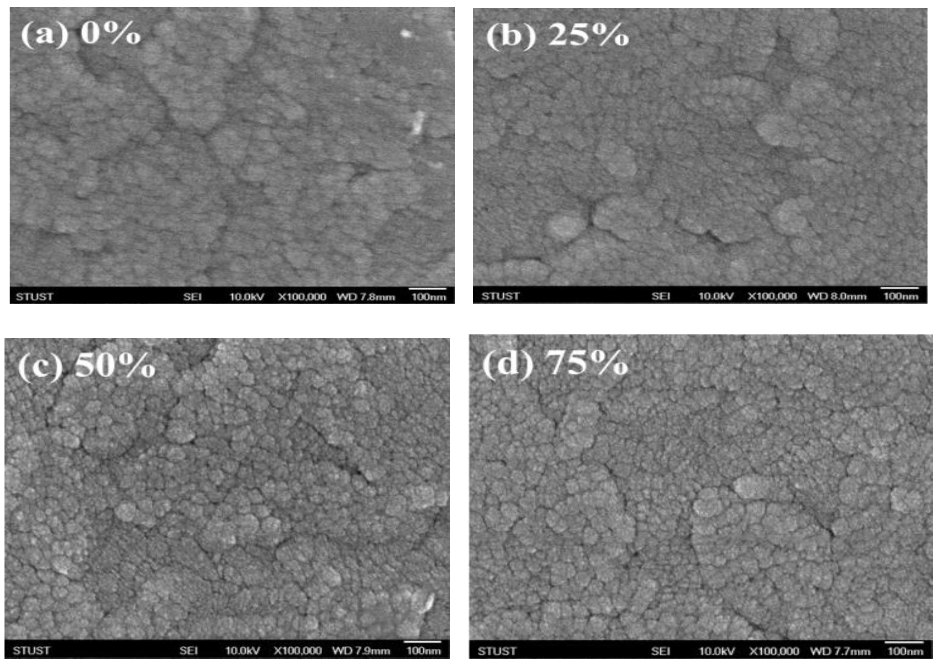
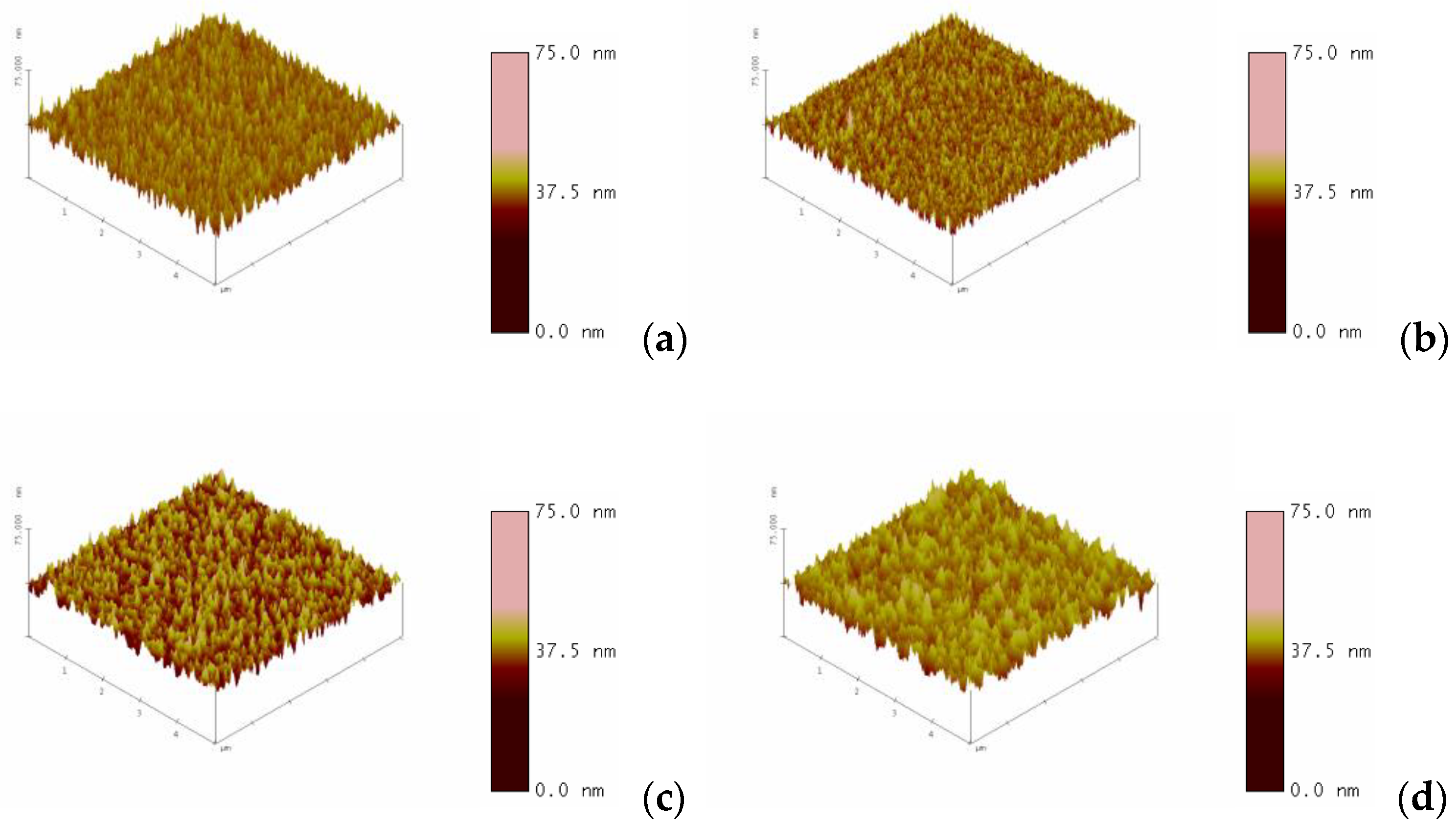
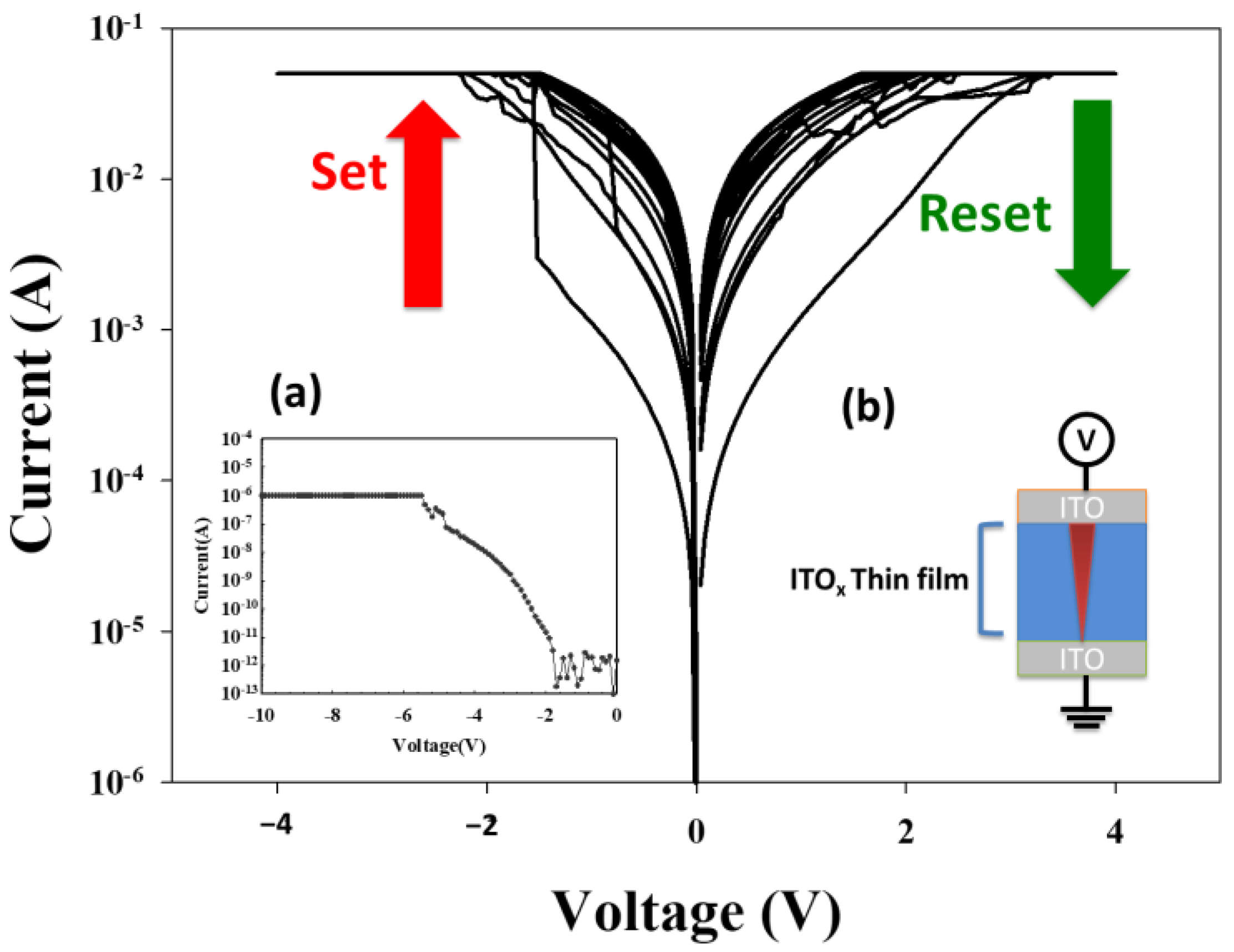
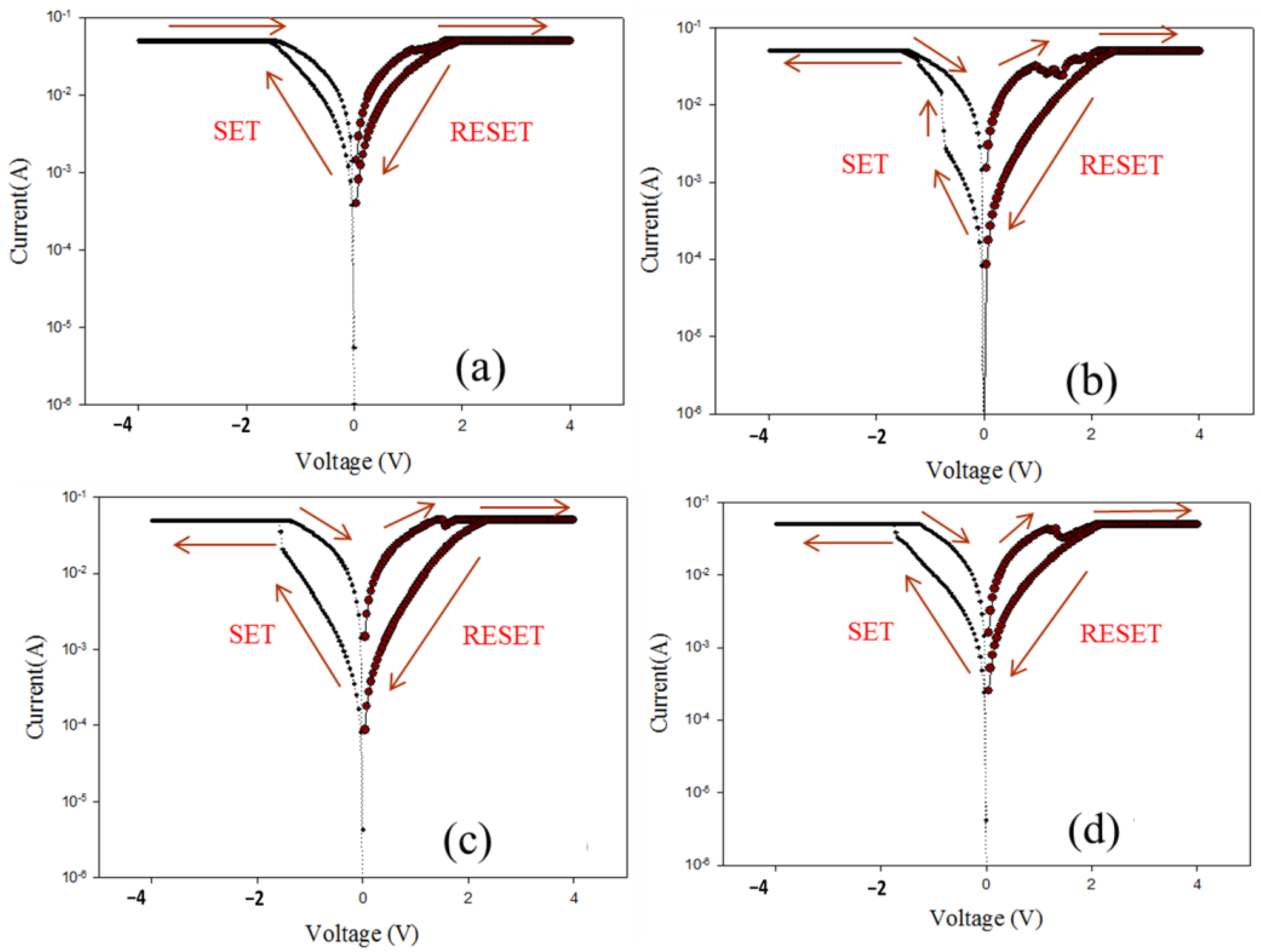
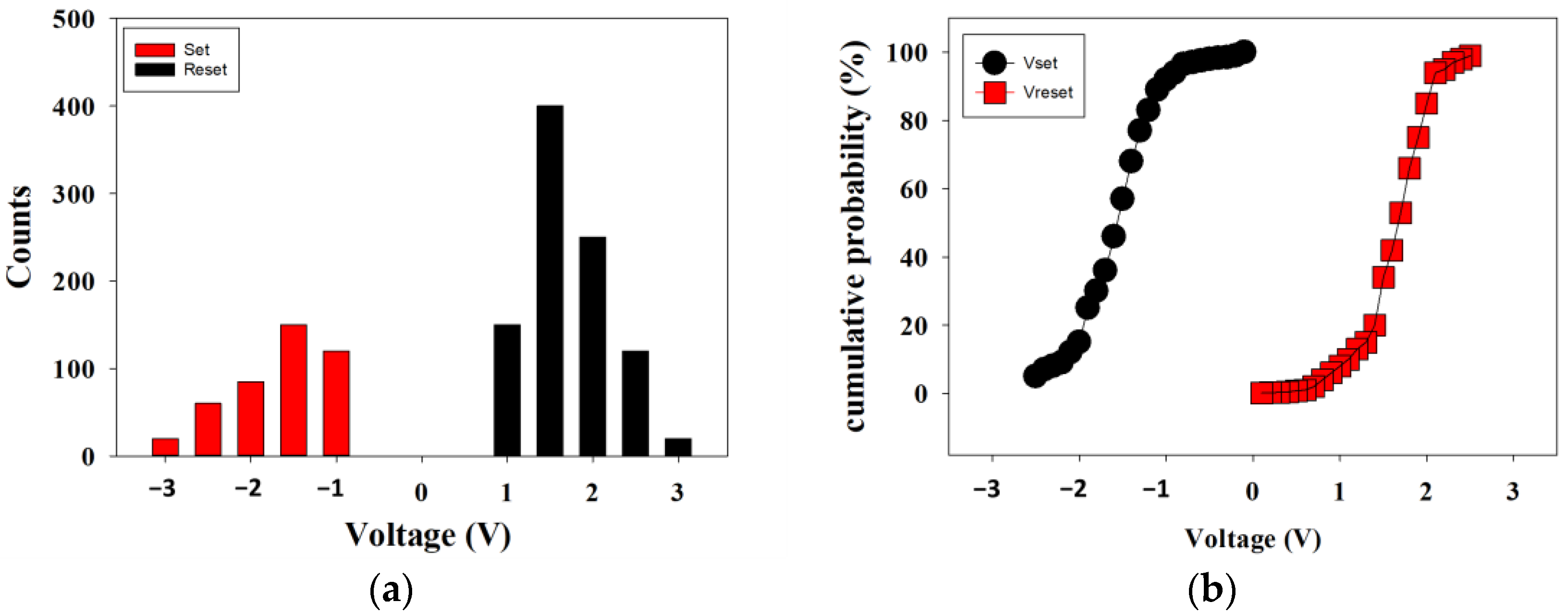
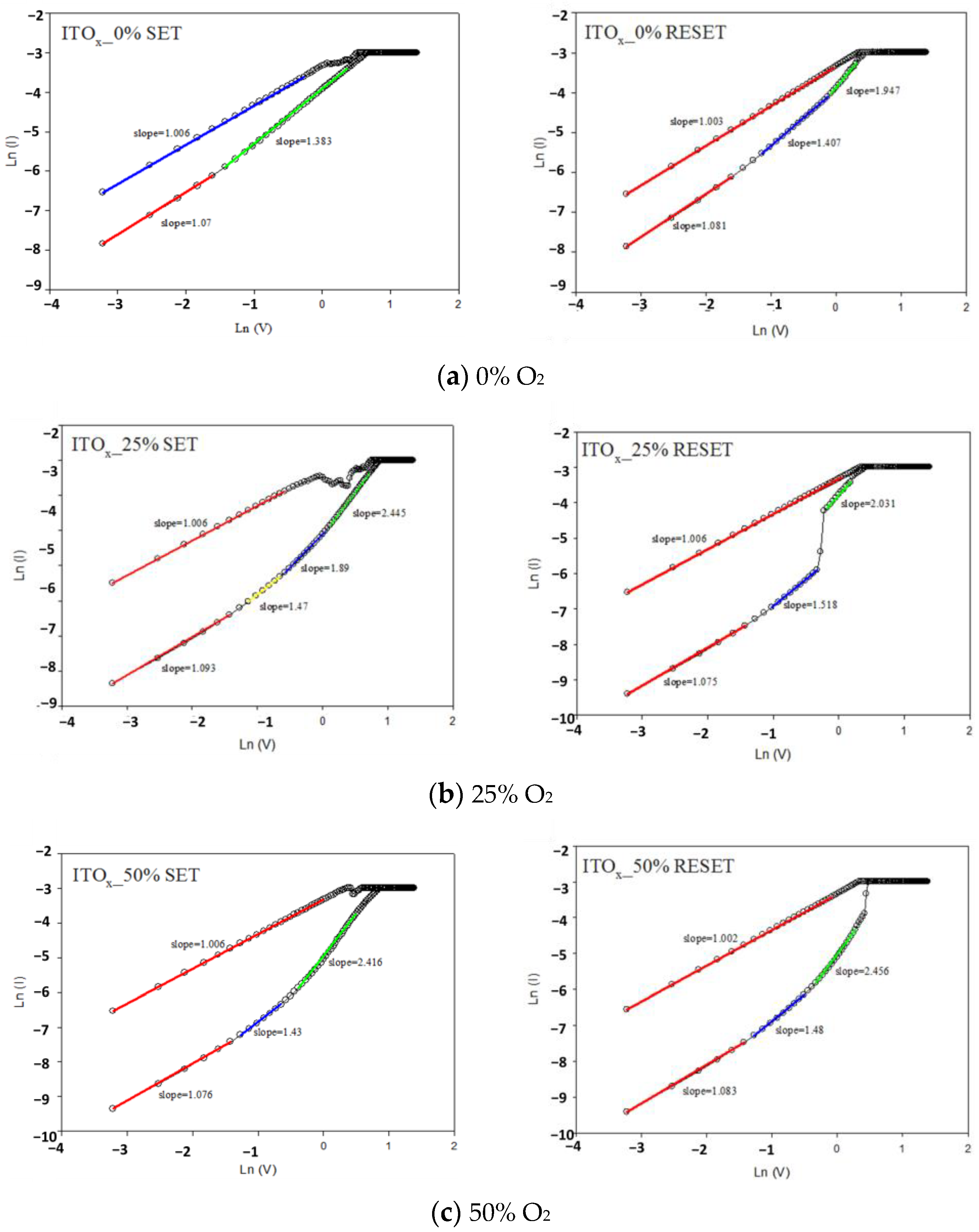
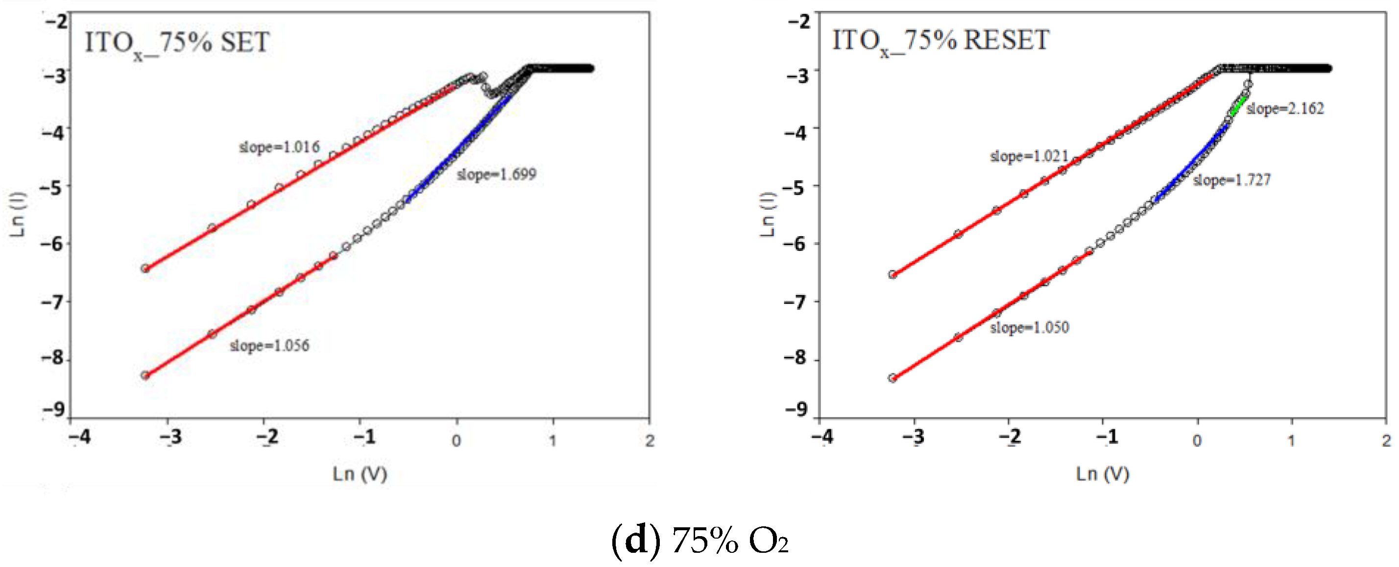
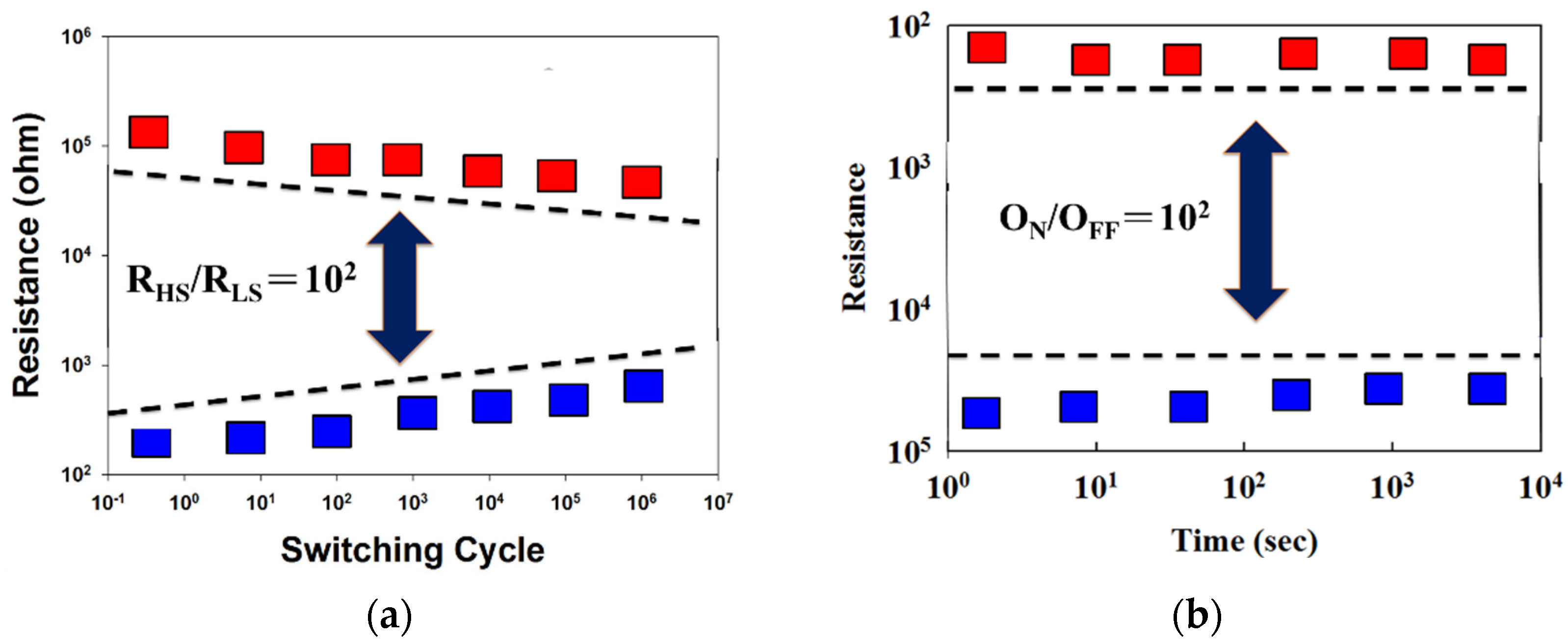
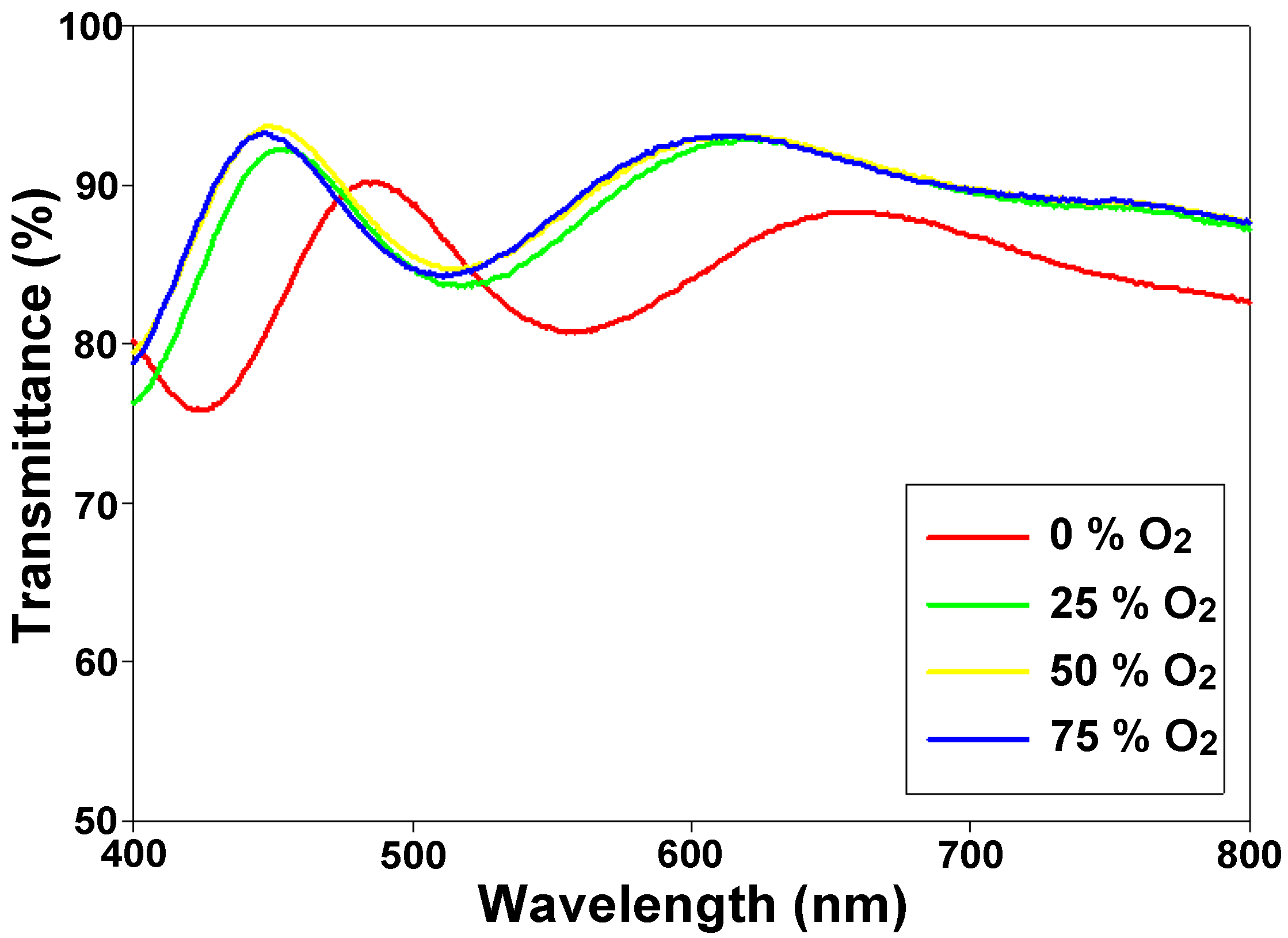
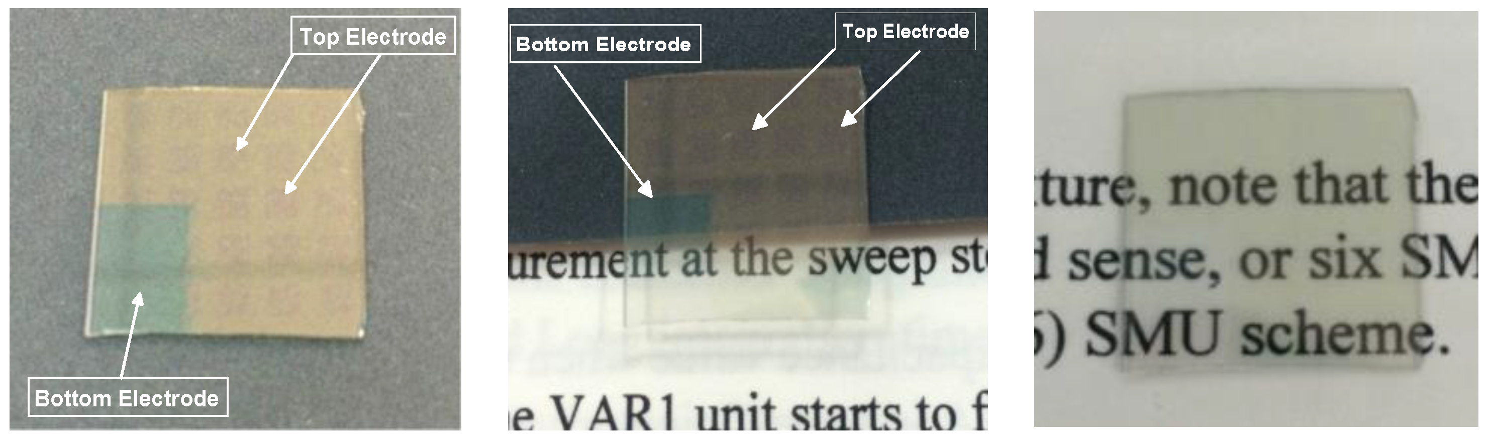
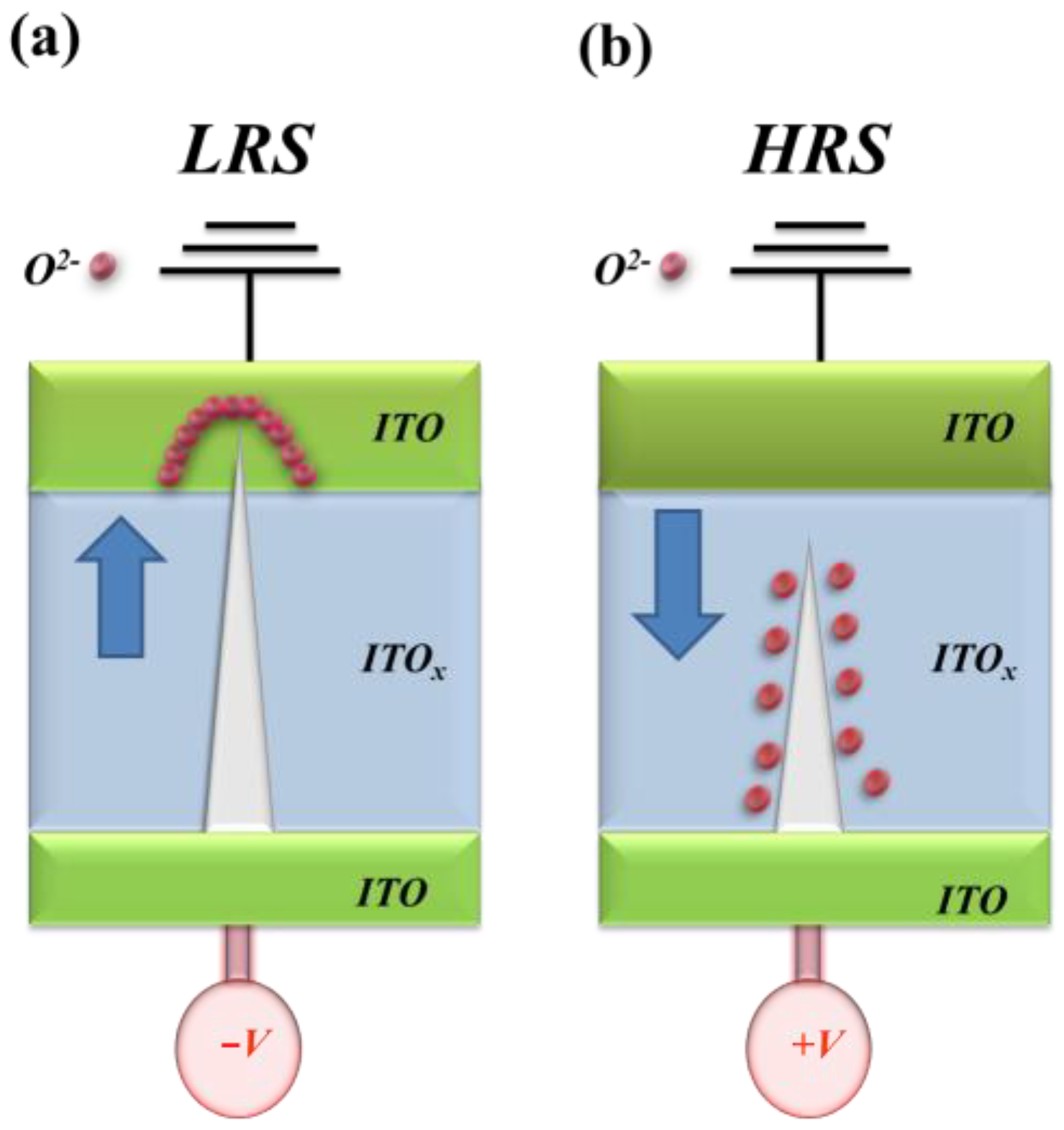
3. Results and Discussion
4. Conclusions
Author Contributions
Funding
Data Availability Statement
Conflicts of Interest
References
- Meijer, G.I. Who wins the nonvolatile memory race? Science 2008, 319, 1625–1626. [Google Scholar] [CrossRef] [PubMed]
- Kim, K.M.; Jeong, D.S.; Hwang, C.S. Nanofilamentary resistive switching in binary oxide system; a review on the present status and outlook. Nanotechnology 2011, 22, 254002. [Google Scholar] [CrossRef] [PubMed]
- Ho, C.H.; Hsu, C.L.; Chen, C.C.; Liu, J.T.; Wu, C.S.; Huang, C.C.; Hu, C.; Yang, F.L. 9nm half-pitch functional resistive memory cell with <1μA programming current using thermally oxidized sub-stoichiometric WOx film. In Proceedings of the 2010 International Electron Devices Meeting (2010 IEDM), San Francisco, CA, USA, 6–8 December 2010; pp. 19.1.1–19.1.4. [Google Scholar] [CrossRef]
- Waser, R.; Aono, M. Nanoionics-based resistive switching memories. Nat. Mater. 2007, 6, 833–840. [Google Scholar] [CrossRef]
- Rahaman, S.Z.; Maikap, S. Low power resistive switching memory using Cu metallic filament in Ge0.2Se0.8 solid-electrolyte. Microelectron. Reliab. 2010, 50, 643–646. [Google Scholar] [CrossRef]
- Choi, S.J.; Lee, J.H.; Bae, H.J.; Yang, W.Y.; Kim, T.W.; Kim, K.H. Improvement of CBRAM resistance window by scaling down electrode size in pure-GeTe film. IEEE Electron Device Lett. 2009, 30, 120–122. [Google Scholar] [CrossRef]
- Goux, L.; Opsomer, K.; Degraeve, R.; Müller, R.; Detavernier, C.; Wouters, D.J.; Jurczak, M.; Altimime, L.; Kittl, J.A. Influence of the Cu-Te composition and microstructure on the resistive switching of Cu-Te/Al2O3/Si cells. Appl. Phys. Lett. 2011, 99, 053502. [Google Scholar] [CrossRef]
- Bernard, Y.; Gonon, P.; Jousseaume, V. Resistance switching of Cu/SiO2Cu/SiO2 memory cells studied under voltage and current-driven modes. Appl. Phys. Lett. 2010, 96, 193502. [Google Scholar] [CrossRef]
- Tsuji, Y.; Sakamoto, T.; Banno, N.; Hada, H.; Aono, M. Off-state and turn-on characteristics of solid electrolyte switch. Appl. Phys. Lett. 2010, 96, 023504. [Google Scholar] [CrossRef]
- Tsunoda, K.; Fukuzumi, Y.; Jameson, J.R.; Wang, Z.; Griffin, P.B.; Nishi, Y. Bipolar resistive switching in polycrystalline TiO2 films. Appl. Phys. Lett. 2007, 90, 113501. [Google Scholar] [CrossRef]
- Choi, H.; Pyun, M.; Kim, T.W.; Hasan, M.; Dong, R.; Lee, J.; Park, J.B.; Yoon, J.; Seong, D.J.; Lee, T.; et al. Nanoscale resistive switching of a Copper-Carbon-Mixed layer for nonvolatile memory applications. IEEE Electron Device Lett. 2009, 30, 302–304. [Google Scholar] [CrossRef]
- Jo, S.H.; Kim, K.H.; Lu, W. High-density crossbar arrays based on a Si memristive system. Nano Lett. 2009, 9, 870–874. [Google Scholar] [CrossRef] [PubMed]
- Seo, J.W.; Park, J.W.; Lim, K.S.; Yang, J.H.; Kang, S.J. Transparent resistive random access memory and its characteristics for nonvolatile resistive switching. Appl. Phys. Lett. 2008, 93, 223505. [Google Scholar] [CrossRef]
- Uprety, K.K.; Ocola, L.E.; Auciello, O. Growth and characterization of transparent Pb(Zi,Ti)O3 capacitor on glass substrate. J. Appl. Phys. 2007, 102, 084107. [Google Scholar] [CrossRef]
- Kudo, A.; Yanagi, H.; Ueda, K.; Hosono, H.; Kawazoe, H.; Yano, Y. Fabrication of transparent p–n heterojunction thin film diodes based entirely on oxide semiconductors. Appl. Phys. Lett. 1999, 75, 2851. [Google Scholar] [CrossRef]
- Kulkarnia, A.K.; Schulzb, K.H.; Lima, T.S.; Khanb, M. Electrical, optical and structural characteristics of indium-tin-oxide thin films deposited on glass and polymer substrates. Thin Solid Film. 1997, 308–309, 1–7. [Google Scholar] [CrossRef]
- Akkad, F.E.; Marafi, M.; Punnoose, A.; Prabu, G. Effect of substrate temperature on the structural, electrical and optical properties of ITO films prepared by RF magnetron sputtering. Phys. Status Solidi (A) 2000, 177, 445–452. [Google Scholar] [CrossRef]
- Choi, S.K.; Lee, J.I. Effect of film density on electrical properties of indium tin oxide films deposited by dc magnetron reactive sputtering. J. Vac. Sci. Technol. A 2001, 19, 2043–2047. [Google Scholar] [CrossRef]
- Fujimoto, M.; Koyama, H.; Konagai, M.; Hosoi, Y.; Ishihara, K.; Ohnishi, S.; Awaya, N. TiO2 anatase nanolayer on TiN thin film exhibiting high-speed bipolar resistive switching. Appl. Phys. Lett. 2006, 89, 223509. [Google Scholar] [CrossRef]
- Seo, S.; Lee, M.J.; Seo, D.H.; Jeoung, E.J.; Suh, D.S.; Joung, Y.S.; Yoo, I.K.; Hwang, I.R.; Kim, S.H.; Byun, I.S.; et al. Reproducible resistance switching in polycrystalline NiO films. Appl. Phys. Lett. 2004, 85, 5655. [Google Scholar] [CrossRef]
- Kim, D.C.; Lee, M.J.; Ahn, S.E.; Seo, S.; Park, J.C.; Yoo, I.K.; Baek, I.G.; Kim, H.J.; Yim, E.K.; Lee, J.E.; et al. Improvement of resistive memory switching in NiO using IrO2. Appl. Phys. Lett. 2006, 88, 232106. [Google Scholar] [CrossRef]
- Oka, T.; Nagaosa, N. InteRFaces of Correlated Electron Systems: Proposed Mechanism for Colossal Electroresistance. Phys. Rev. Lett. 2005, 95, 266403. [Google Scholar] [CrossRef] [PubMed]
- Choi, B.J.; Jeong, D.S.; Kim, S.K.; Rohde, C.; Choi, S.; Oh, J.H.; Kim, H.J.; Hwang, C.S.; Szot, K.; Waser, R.; et al. Resistive switching mechanism of TiO2 thin films grown by atomic-layer deposition. J. Appl. Phys. 2005, 98, 033715. [Google Scholar] [CrossRef]
- Jeon, S.H.; Park, B.H.; Lee, J.; Lee, B.; Han, S. First-principles modeling of resistance switching in perovskite oxide material. Appl. Phys. Lett. 2006, 89, 042904. [Google Scholar] [CrossRef]
- Rozenberg, M.J.; Inoue, I.H.; Sanchez, M.J. Strong electron correlation effects in nonvolatile electronic memory devices. Appl. Phys. Lett. 2006, 88, 033510. [Google Scholar] [CrossRef]
- Sze, S.M. Physics of Semiconductor Devices, 2nd ed.; Wiley: New York, NY, USA, 1981; p. 403. ISBN 0-471-05661-8. [Google Scholar]


| Mole fraction | Sn | In | O |
|---|---|---|---|
| ITO | 5.08% | 47.76% | 47.15% |
| RTA-ITO | 4.7% | 18.32% | 76.98% |
| Growth Procedure Argon: Oxygen Gas (%) | Thin Film Oxygen Mole Fraction (%) |
|---|---|
| 0% | 47.15% |
| 25% | 52.1% |
| 50% | 55.2% |
| 75% | 57.4% |
Disclaimer/Publisher’s Note: The statements, opinions and data contained in all publications are solely those of the individual author(s) and contributor(s) and not of MDPI and/or the editor(s). MDPI and/or the editor(s) disclaim responsibility for any injury to people or property resulting from any ideas, methods, instructions or products referred to in the content. |
© 2023 by the authors. Licensee MDPI, Basel, Switzerland. This article is an open access article distributed under the terms and conditions of the Creative Commons Attribution (CC BY) license (https://creativecommons.org/licenses/by/4.0/).
Share and Cite
Chen, K.-H.; Cheng, C.-M.; Chen, M.-L.; Pan, Y.-Y. Bipolar Switching Properties of the Transparent Indium Tin Oxide Thin Film Resistance Random Access Memories. Nanomaterials 2023, 13, 688. https://doi.org/10.3390/nano13040688
Chen K-H, Cheng C-M, Chen M-L, Pan Y-Y. Bipolar Switching Properties of the Transparent Indium Tin Oxide Thin Film Resistance Random Access Memories. Nanomaterials. 2023; 13(4):688. https://doi.org/10.3390/nano13040688
Chicago/Turabian StyleChen, Kai-Huang, Chien-Min Cheng, Mei-Li Chen, and Yi-Yun Pan. 2023. "Bipolar Switching Properties of the Transparent Indium Tin Oxide Thin Film Resistance Random Access Memories" Nanomaterials 13, no. 4: 688. https://doi.org/10.3390/nano13040688
APA StyleChen, K.-H., Cheng, C.-M., Chen, M.-L., & Pan, Y.-Y. (2023). Bipolar Switching Properties of the Transparent Indium Tin Oxide Thin Film Resistance Random Access Memories. Nanomaterials, 13(4), 688. https://doi.org/10.3390/nano13040688