Abstract
The rough morphology at the growth surface results in the non-uniform distribution of indium composition, intentionally or unintentionally doped impurity, and thus impacts the performance of GaN-based optoelectronic and vertical power electronic devices. We observed the morphologies of unintentionally doped GaN homo-epitaxially grown via MOCVD and identified the relations between rough surfaces and the miscut angle and direction of the substrate. The growth kinetics under the effect of the Ehrlich–Schwoebel barrier were studied, and it was found that asymmetric step motions in samples with a large miscut angle or those grown at high temperature were the causes of step-bunching. Meandering steps were believed to be caused by surface free energy minimization for steps with wide terraces or deviating from the m-direction.
1. Introduction
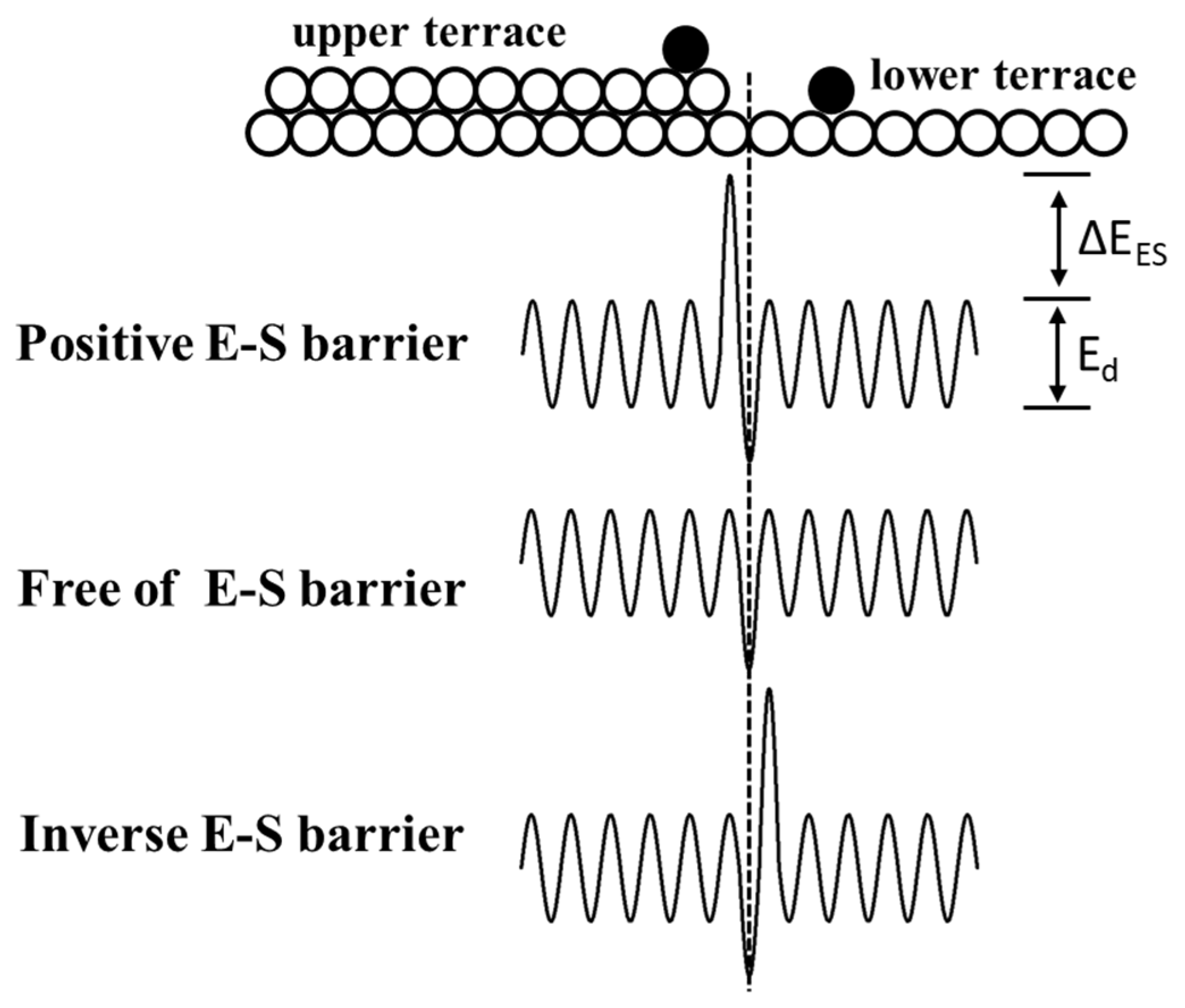
Nowadays, GaN is receiving more and more attention due to its application prospects in electronic and optoelectronic devices. The application of high-quality freestanding GaN substrate is essential in further improving device performance for devices such as laser diodes and vertical power diodes [1,2,3,4,5,6,7]. However, numerous studies have revealed that device performance deteriorates due to the rough surfaces induced by meandering steps and macro-steps tens of monolayers high. Kizilyalli et al. found that the wavy morphology of homo-epitaxially grown GaN Shottky diodes and p-n diodes grown via MOCVD caused large current non-uniformities [8]. Hayashi et al. discovered that a striped morphology induced a current-crowding effect in vertical GaN p-n junction diodes [9]. GaN layers are often used as the basis for low-dimensional InGaN/GaN heterostructures. Indium composition fluctuations caused by a rough surface have been observed by many researchers, using measurements such as cathodoluminescence mapping [10,11,12,13,14,15] and scanning near-field optical microscopy [16]. According to Bales and Zangwill, wavy surfaces including meandering and bunching steps are mostly caused by morphological instabilities under the effect of adatom incorporation asymmetry at the steps [17]. Generally, the energy barrier for adatom crossing over a step is called the E-S barrier and can be classified into three types, as shown in Figure 1 [18,19,20]. Many results based on Monte Carlo simulations have verified that steps under an inverse E-S barrier easily bunch to form macro-steps [21,22,23,24,25]. However, the relations among the E-S barrier, miscut, and step instabilities are rarely studied with a focus on the aspect of growth kinetics. In this work, we found the relations between miscut and step instabilities in unintentionally doped GaN grown via MOCVD. The step kinetics affected by the E-S barrier were studied based on the step motion model proposed by Schwoebel and Shipsey [20,26]. The steps with wider terraces and those propagating toward directions deviating from the m-axis were believed to be unstable.

Figure 1.
The energy barrier ΔEES for adatoms at the upper terrace (positive) or at the lower terrace (inverse) to overcome when incorporated into the step. There is no E-S barrier when the incorporation possibility for adatoms from both sides of the step is equal. Ed is the diffusion barrier energy.
2. Materials and Methods
The GaN substrate used in this paper has threading dislocation density of the about 106 cm−2 and bow of 15 μm. The misorientation angle (also called miscut angle) and directions are nonuniform across the 2-inch substrate due to the crystalline bowing during substrate epitaxy, and hence the miscut angle varies from 0.22° to 0.55°. Therefore, the effect of miscuts on homo-epi GaN morphology can be studied on such a GaN substrate with quite different miscuts in different areas. Unintentionally doped GaN (uGaN) films with a thickness of about 100 nm were grown twice, subsequently, at different growth temperatures using a metalorganic chemical vapor deposition (MOCVD) reactor. Trimethylgallium (TMGa) and ammonia were used as source gases, while hydrogen was used as carrier gas. The local miscut information was obtained via the analysis of XRD rocking curves by rotating the substrate around surface normal. Surface morphologies were studied using an atomic force microscope (AFM, Bruker Dimension ICON, Billerica, MA, USA) in tapping mode. AFM amplitude images were used to clearly show atomic step features even on a surface tens of microns large, with large height differences.
3. Results
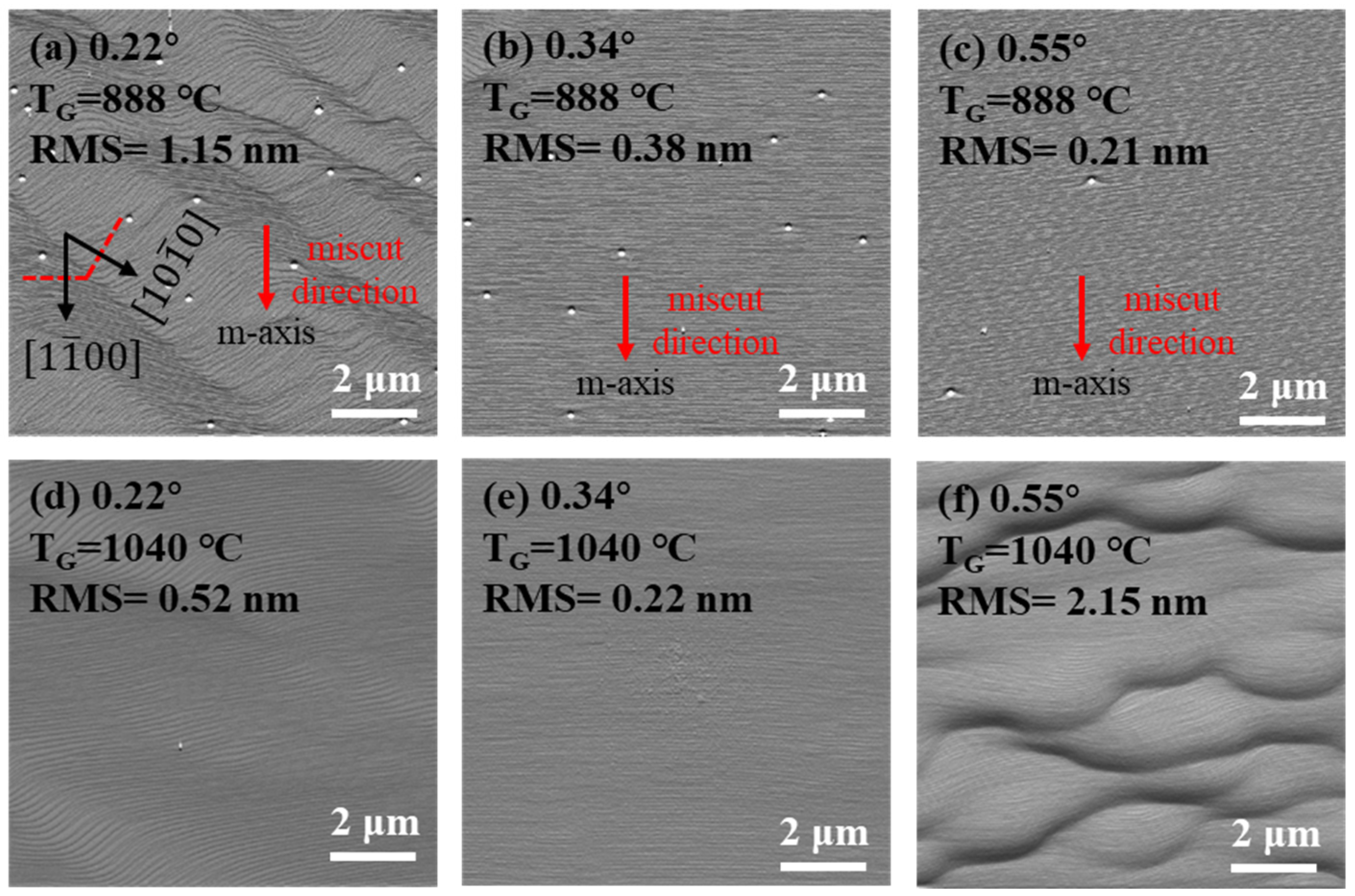
AFM images of samples grown at different temperature in the areas with a different miscut angle toward the m-direction are shown in Figure 2. At 888 °C, the surface morphology of uGaN in the area with a miscut angle of 0.22° features meandering steps, as shown in Figure 2a, which consist of steps perpendicular to the m-direction with a terrace width of about 45 nm and steps perpendicular to the m-direction with a terrace width of about 76 nm. The spacing between interlacing steps seems to be random. For the areas with a larger miscut angle, the surface morphologies show uniform and straight atomic steps, as shown in Figure 2b,c. The average terrace widths in both areas agree well with the miscut angle. For samples grown at 1040 °C, V-pits induced by threading dislocations disappear. The surface in the area with a miscut angle of 0.34° maintains a step-flow morphology and has a decrease in roughness due to the elimination of V-pits. The surface in the area with a miscut angle of 0.22° is smoother due to the suppression of the step-meandering phenomenon, as shown in Figure 2d. In contrast, step-bunching with a maximum step height of about 9.7 nm takes place in the area with a miscut angle of 0.55°, as shown in Figure 2f. This is a very common phenomenon for surfaces with narrower terraces due to the increased miscut angle.

Figure 2.
This figure shows 10 × 10 μm2 AFM amplitude images of uGaN surfaces at the areas with different miscut angles toward the m-direction. The first line of the images is taken after first growth at a growth temperature of 888 °C, while the second line is taken after second growth at 1040 °C. (a,d) 0.22°; (b,e) 0.34°; (c,f) 0.55°.
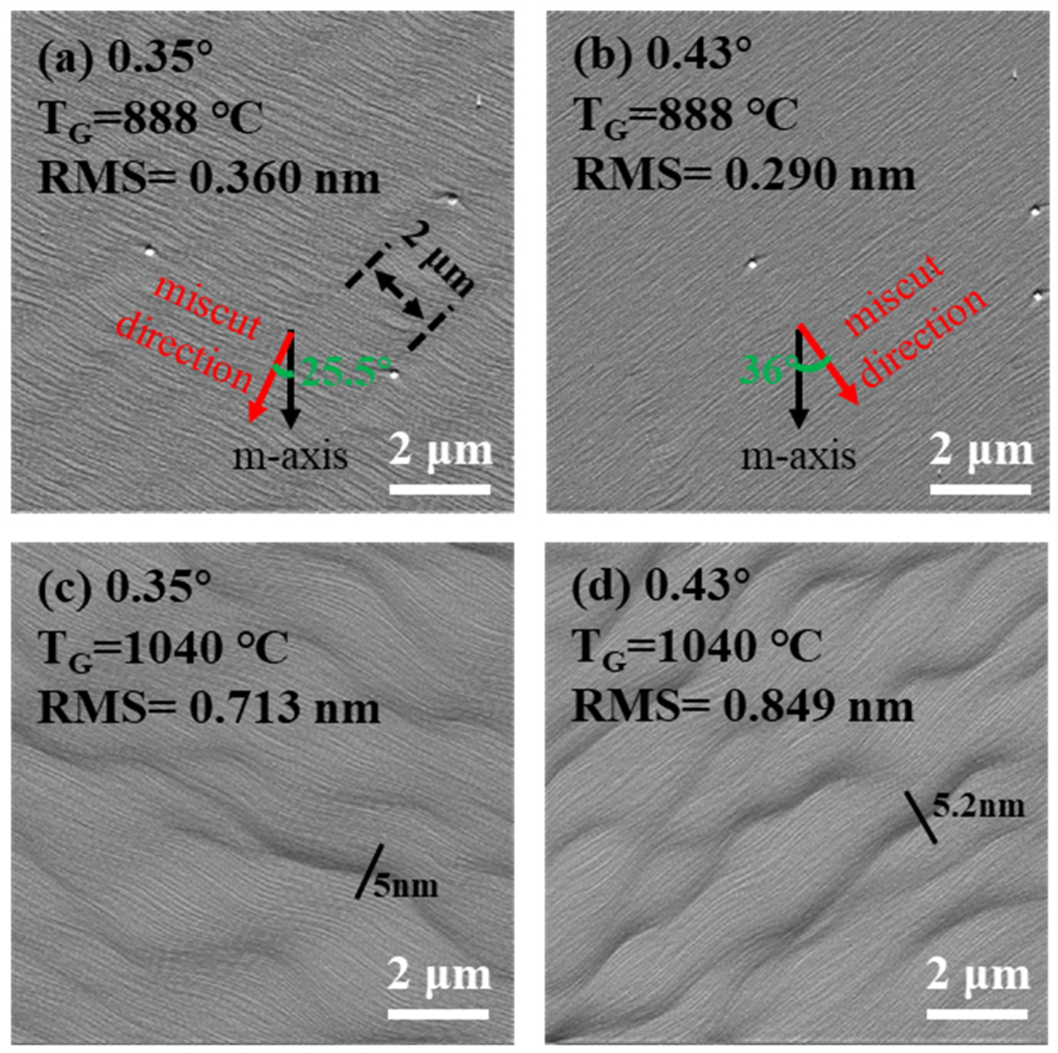
Figure 3 shows the morphology in the area misoriented toward the direction deviating from the m-direction. The wave-shaped steps in Figure 3a also suggests a slight step-meandering phenomenon with quite a uniform spacing of interlacing steps, of about 2 μm. For the area with a larger miscut angle (0.43°) misoriented toward the direction deviating 36° from the m-direction, the step-flow morphology with uniform and straight terraces is shown in Figure 3b. At the growth temperature of 1040 °C, both areas with miscut angles of 0.35° and 0.43° show a step-bunching morphology. The maximum height of bunched steps is 5 nm for the area with a miscut angle of 0.35° and 5.2 nm for the area with a miscut angle of 0.43°.

Figure 3.
This figure shows 10 × 10 μm2 AFM amplitude images of uGaN surfaces in the areas with different miscut angles deviated from the m-direction. The first line of the images is taken after first growth at a growth temperature of 888 °C, while the second line is taken after second growth at 1040 °C. (a,c) 0.34° toward (−a + m)-direction; (b,d) 0.43° toward (a + m)-direction.
By combining our analysis of Figure 2 and Figure 3, we can see that areas with a miscut angle larger than 0.34° all show a step-bunching morphology when grown at 1040 °C. The larger the miscut angle, the rougher the surface according to the RMS values. Moreover, the height differences of the bunched steps are bigger in the area with a larger miscut angle. Hence, the morphological instability induced by step bunching is more severe at a larger miscut angle. The morphological difference in Figure 2e and Figure 3c suggests that meandering steps are more easily bunched than straight steps under the same growth condition. Comparing all AFM images of uGaN grown at 888 °C, we can conclude that the step-meandering phenomenon easily occurs at the surfaces of steps with wider terraces or deviating from the m-direction and can be effectively suppressed by increasing the growth temperature.
4. Discussion
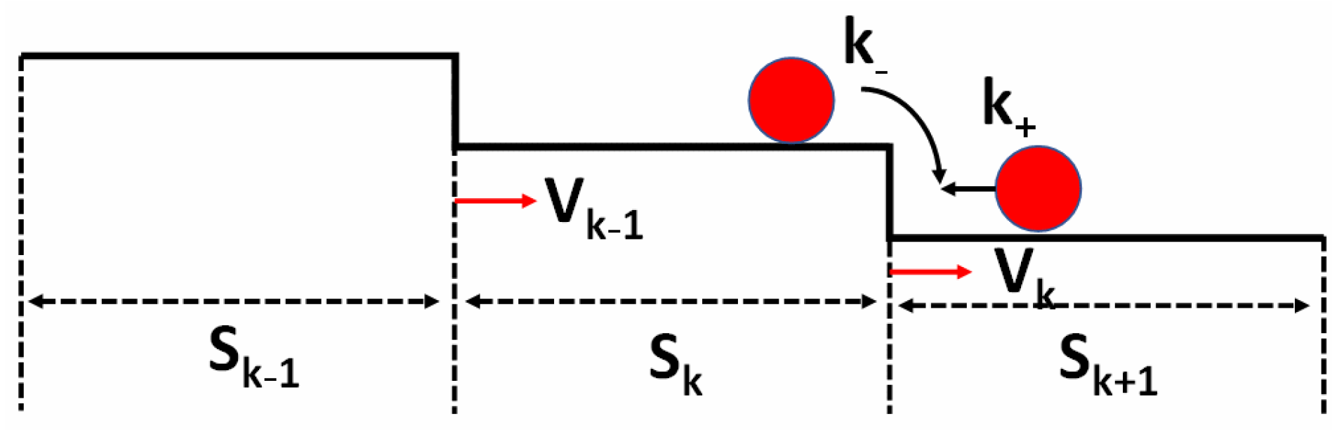
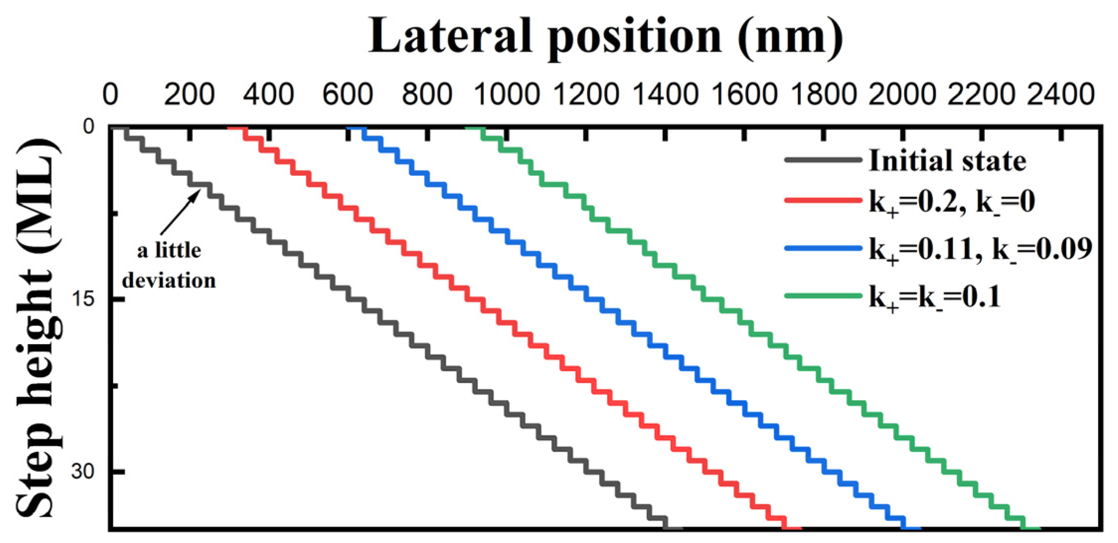
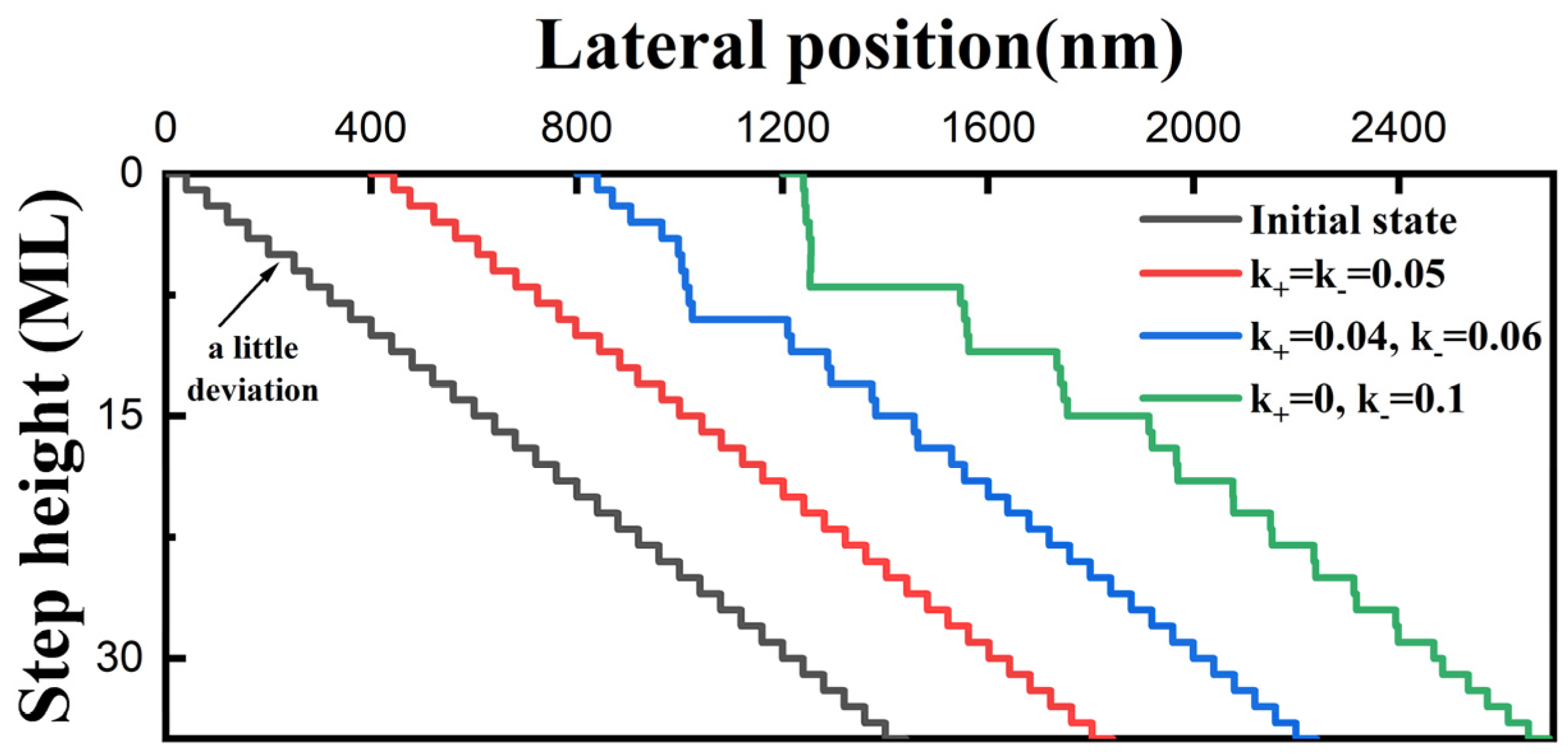
To explain the relations between the step-bunching morphology and the miscut angle, we applied the step motion model introduced by Schwoebel and Shipsey to study step kinetics under the effect of the E-S barrier [20]. The detailed simulated parameters can be found in our previous paper [27]. As shown in Figure 4, only a small portion of adatoms reaching the step can be incorporated into the step due to behaviors such as reflection from the step, transmission across the step, and diffusion along the step [28]. Hence, the incorporation probability of adatoms from the lower terrace is defined as k+, while that from the upper terrace is defined as k−. Under a positive E-S barrier, the adatoms from the upper terrace have more difficulty being incorporated at the step, which makes k+ larger than k−. While the E-S barrier occurs at the lower terrace (inverse), k+ is smaller than k−. There is no E-S barrier when k+ equals k−. When the widths of all terraces are equal at the initiate state, all steps advance at the same speed and remain unaffected by the E-S barrier and adatom diffusion length. However, the above ideal situation does not occur, and the terraces of steps fluctuate around the average value on the real surfaces. Therefore, a little deviation is applied to one of the steps to make it travel 1/4 of the average terrace width in the initial state.

Figure 4.
Step motion model on a vicinal surface. vk is the velocity of the kth step, while the width of its upper and lower terrace is sk and sk−1, respectively. k+ and k− represent the adatom incorporation probability from the lower and upper terraces, respectively. vk+1 and sk+1 represent the velocity of the (k + 1)th step and the width of its lower terrace.
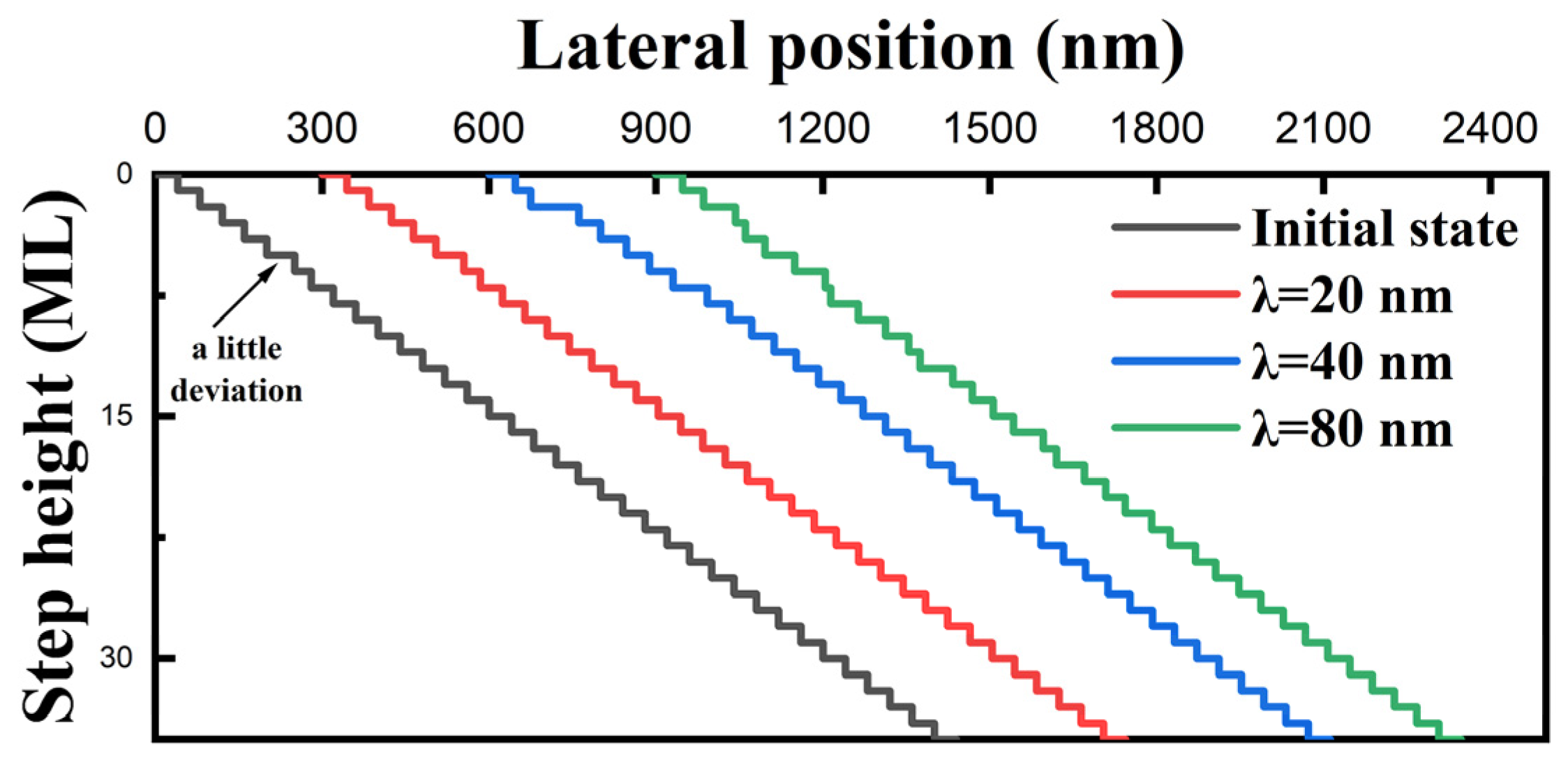
Figure 5 shows the simulated results under the circumstances of there being no E-S barrier with a different adatom diffusion length. When the adatom diffusion length is insufficient in the red line, the effect of the intentionally introduced deviation is concealed because the steps maintain the same speed. The terrace around the deviated step tends to broaden or narrow in the blue line when the adatom diffusion length is equal to the average terrace width. Step bunching occurs with a much larger adatom diffusion length, as shown via the green line. Therefore, the effects of the E-S barrier and the deviation in the terrace width are more significant with a larger adatom diffusion length.
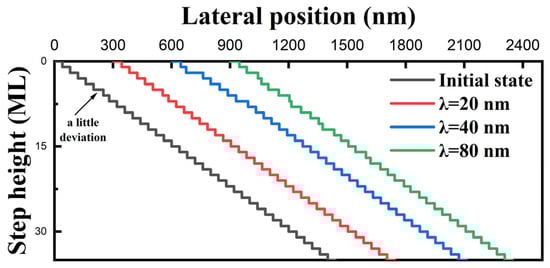
Figure 5.
Simulated results with a different adatom diffusion length when there is no E-S barrier (k+ = k− = 0.1).
In the following simulations, the adatom diffusion length is set to be double that of the average terrace width to clearly observe the effect of the E-S barrier. The higher the E-S barrier height, the greater the difference in adatom incorporation probability from the lower and upper terrace. Hence, we can adjust the value of k+ and k− to study the effect of different E-S barrier heights. As shown in Figure 6, step bunching occurs under the circumstance of a free E-S barrier (green line), while it disappears under the circumstance of a relatively low positive E-S barrier (blue line). When it comes to the extreme case that no adatoms at the upper terrace can overcome the E-S barrier (red line), the terrace widths of all steps become equal. This obviously shows that a relatively large positive E-S barrier is helpful in suppressing fluctuations in the terrace width and creates a stable surface morphology. In contrast, steps easily bunch with an inverse E-S barrier, as shown in Figure 7. The maximal layers of bunched steps rapidly increase with the height of the inverse E-S barrier (5 for the blue line and 8 for the green line).
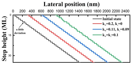
Figure 6.
Simulated results showing the effect of a positive E-S barrier on step motions (λ = 80 nm). The green line is under the circumstance that there is no E-S barrier, while the red line is under an extreme case when the energy barrier at the upper terrace is so large that no adatoms can cross over and be incorporated into the step. A relatively small E-S barrier is set for the blue line.
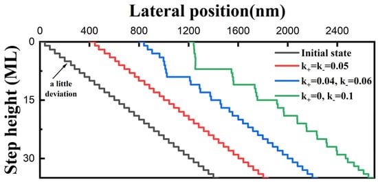
Figure 7.
Simulated results showing the effects of an inverse E-S barrier on step motions (λ = 80 nm). The red line is under the circumstance of there being no E-S barrier, while the green line is in an extreme case where the energy barrier at the lower terrace is so large that no adatoms can cross over and be incorporated into the step. A relatively small E-S barrier is set for the blue line.
According to many studies, both the adatom diffusion length λ and the E-S barrier are closely related to growth conditions, such as the temperature [29,30,31]. According to Einstein’s relation [32],
where D is the diffusion coefficient, τ is the mean time of surface diffusion, λ0 is a merged effective elementary jump distance, kB is the Boltzmann constant, T is the growth temperature, Ea is the absorption energy and equal to the barrier to be surmounted for desorption, and Ed is the energy barrier for diffusion. In MOCVD, GaN epitaxy is maintained in a diffusion-limited regime, which is grown at a low temperature, much lower than the temperature for evaporation. Therefore, Ea is usually much larger than Ed and also several times larger than the thermal energies kBT. The desorption of adatoms becomes negligible, and the residence time is large. Hence, λ is proportional to −Ed/(2kBT) and, consequently, the adatom diffusion length is positively related to the growth temperature. The positive E-S barrier can be lowered by an increased temperature and can lead to a growth mode transition from island to step-flow. Hence, the elevated growth temperature increases the adatom diffusion length and lowers the positive E-S barrier or even makes it inverse, resulting in more adatoms from the upper terrace being incorporated into the steps and forming a step-bunching morphology [33].
Regarding the step-meandering phenomenon, the one-dimensional step motion model mentioned above is not applicable, and hence it is discussed qualitatively. In general, meandered steps can be caused by extrinsic perturbations at the surface, such as defects, impurities, or local fluctuation, or by intrinsic perturbations, such as the E-S barrier and surface tension [11]. The extrinsic perturbations are irregular and randomly distributed, and thus we focus on the influence of the E-S barrier and surface tension. Numerous theoretical studies have shown that the existence of the E-S barrier aggravates the fluctuation of the step shape [17,34,35,36,37,38,39]. According to Jeong and Williams, the surface free energy γα can be described by the free energy of the terrace γ0, the free energy of the step β, and the step–step interaction g as a function of the miscut angle α in the following way [40]:
where h represents the atomic step height of a half-unit cell. For a misoriented surface, it can adjust the dangling bonds on the terraces and at the steps or modulate the kink distributions along the steps to make it energetically favorable in specific growth conditions. However, this kind of change may be insufficient sometimes, such as for surfaces covered by ultra-wide terraces or steps with a large amount of free energy. In this case, the surface will break up into facets of the neighboring orientations that are represented in the equilibrium crystal shape [41]. According to the crystal structure of GaN, steps toward the m-direction and its equivalent directions have the lowest energy [42]. Therefore, the free energy of steps deviated from the m-direction β’ is much larger than that toward the m-direction β. On the other hand, the free energy of terraces is proportional to their width. Hence, the free energy of wide terraces γ0′ is much larger than that of narrow terraces γ0. Therefore, steps deviated from the m-direction or with wide terraces are unstable and readily swerve into neighboring orientations or form meandering edges.
5. Conclusions
In summary, the surface morphologies of unintentionally doped GaN are observed in the freestanding substrate with different miscut angles and miscut directions. Step instabilities including step meandering and step bunching are found to be associated with the miscut angle, miscut direction, and growth temperature. Bunched steps are easily generated in samples with a large miscut angle or those grown at a high temperature. According to the simulated results, increasing the growth temperature results in a longer adatom diffusion length, accompanied by changes in the E-S barrier, which makes it easy for step bunching to occur. Steps with wide terraces or those deviating from m-direction are believed to have a higher free energy and, hence, easily meander. These findings indicate that a substrate miscut angle and direction and growth conditions are essential in obtaining a smooth surface.
Author Contributions
Conceptualization, H.Y. and M.I.; methodology, P.W., F.L., F.Z., X.L., B.Z. and X.R.; validation, A.T.; resources, W.Z.; writing—original draft preparation, P.W.; writing—review and editing, J.L.; supervision, H.Y. and J.L. All authors have read and agreed to the published version of the manuscript.
Funding
This work was supported by the National Key Research and Development Program of China (2022YFB2802801, 2017YFE0131500), the National Natural Science Foundation of China (61834008, U21A20493), and the Key Research and Development Program of Jiangsu Province (BE2020004, BE2021008-1).
Data Availability Statement
The data presented in this study are available on request from the corresponding author.
Acknowledgments
The authors are grateful for technical support from Nano-X and Nano Fabrication Facility from Suzhou Institute of Nano-Tech and Nano-Bionics, Chinese Academy of Sciences (SINANO).
Conflicts of Interest
The authors declare no conflicts of interest.
References
- Hu, L.; Ren, X.; Liu, J.; Tian, A.; Jiang, L.; Huang, S.; Zhou, W.; Zhang, L.; Yang, H. High-Power Hybrid GaN-Based Green Laser Diodes with ITO Cladding Layer. Photon. Res. 2020, 8, 279. [Google Scholar] [CrossRef]
- Tian, A.; Hu, L.; Zhang, L.; Liu, J.; Yang, H. Design and Growth of GaN-Based Blue and Green Laser Diodes. Sci. China Mater. 2020, 63, 1348. [Google Scholar] [CrossRef]
- Tian, A.; Hu, L.; Li, X.; Wu, S.; Xu, P.; Wang, D.; Zhou, R.; Guo, B.; Li, F.; Zhou, W.; et al. Greatly Suppressed Potential Inhomogeneity and Performance Improvement of C-Plane InGaN Green Laser Diodes. Sci. China Mater. 2022, 65, 543. [Google Scholar] [CrossRef]
- Jiang, L.; Liu, J.; Tian, A.; Cheng, Y.; Li, Z.; Zhang, L.; Zhang, S.; Li, D.; Ikeda, M.; Yang, H. GaN-Based Green Laser Diodes. J. Semicond. 2016, 37, 111001. [Google Scholar] [CrossRef]
- Kaneko, S.; Kuroda, M.; Yanagihara, M.; Ikoshi, A.; Okita, H.; Morita, T.; Tanaka, K.; Hikita, M.; Uemoto, Y.; Takahashi, S.; et al. Current-Collapse-Free Operations up to 850 V by GaN-GIT Utilizing Hole Injection from Drain. In Proceedings of the 2015 IEEE 27th International Symposium on Power Semiconductor Devices & IC’s (ISPSD), Hong Kong, China, 10–14 May 2015; pp. 41–44. [Google Scholar]
- Yamada, H.; Iso, K.; Saito, M.; Fujito, K.; DenBaars, S.P.; Speck, J.S.; Nakamura, S. Impact of Substrate Miscut on the Characteristic of M-Plane InGaN/GaN Light Emitting Diodes. Jpn. J. Appl. Phys. 2007, 46, L1117. [Google Scholar] [CrossRef]
- Lin, Y.-D.; Hardy, M.T.; Hsu, P.S.; Kelchner, K.M.; Huang, C.-Y.; Haeger, D.A.; Farrell, R.M.; Fujito, K.; Chakraborty, A.; Ohta, H.; et al. Blue-Green InGaN/GaN Laser Diodes on Miscut m-Plane GaN Substrate. Appl. Phys. Express 2009, 2, 082102. [Google Scholar] [CrossRef]
- Kizilyalli, I.C.; Bui-Quang, P.; Disney, D.; Bhatia, H.; Aktas, O. Reliability Studies of Vertical GaN Devices Based on Bulk GaN Substrates. Microelectron. Reliab. 2015, 55, 1654. [Google Scholar] [CrossRef]
- Hayashi, K.; Ohta, H.; Horikiri, F.; Narita, Y.; Yoshida, T.; Mishima, T. Direct Observation of High Current Density Area by Microscopic Electroluminescence Mapping in Vertical GaN p–n Junction Diodes. Phys. Status Solidi (a) 2018, 215, 1700501. [Google Scholar] [CrossRef]
- Kelchner, K.M.; Kuritzky, L.Y.; Fujito, K.; Nakamura, S.; DenBaars, S.P.; Speck, J.S. Emission Characteristics of Single InGaN Quantum Wells on Misoriented Nonpolar M-Plane Bulk GaN Substrates. J. Cryst. Growth 2013, 382, 80. [Google Scholar] [CrossRef]
- Kelchner, K.M.; Kuritzky, L.Y.; Nakamura, S.; DenBaars, S.P.; Speck, J.S. Stable Vicinal Step Orientations in M-Plane GaN. J. Cryst. Growth 2015, 411, 56. [Google Scholar] [CrossRef]
- Zeimer, U.; Jeschke, J.; Mogilatenko, A.; Knauer, A.; Kueller, V.; Hoffmann, V.; Kuhn, C.; Simoneit, T.; Martens, M.; Wernicke, T.; et al. Spatial Inhomogeneities in AlxGa1-xN Quantum Wells Induced by the Surface Morphology of AlN/Sapphire Templates. Semicond. Sci. Technol. 2015, 30, 114008. [Google Scholar] [CrossRef]
- Zhou, K.; Liu, J.; Ikeda, M.; Zhang, S.; Li, D.; Zhang, L.; Zeng, C.; Yang, H. Influence of Substrate Surface Defects on the Homoepitaxial Growth of GaN (0001) by Metalorganic Vapor Phase Epitaxy. J. Cryst. Growth 2015, 416, 175. [Google Scholar] [CrossRef]
- Nakamura, A.; Yanagita, N.; Murata, T.; Hoshino, K.; Tadatomo, K. Effects of Sapphire Substrate Misorientation on the GaN-based Light Emitting Diode Grown by Metalorganic Vapour Phase Epitaxy. Phys. Status Solidi (c) 2008, 5, 2007. [Google Scholar] [CrossRef]
- Kryśko, M.; Franssen, G.; Suski, T.; Albrecht, M.; Łucznik, B.; Grzegory, I.; Krukowski, S.; Czernecki, R.; Grzanka, S.; Makarowa, I.; et al. Correlation between Luminescence and Compositional Striations in InGaN Layers Grown on Miscut GaN Substrates. Appl. Phys. Lett. 2007, 91, 211904. [Google Scholar] [CrossRef]
- Uždavinys, T.K.; Marcinkevičius, S.; Mensi, M.; Lahourcade, L.; Carlin, J.-F.; Martin, D.; Butté, R.; Grandjean, N. Impact of Surface Morphology on the Properties of Light Emission in InGaN Epilayers. Appl. Phys. Express 2018, 11, 051004. [Google Scholar] [CrossRef]
- Bales, G.S.; Zangwill, A. Morphological Instability of a Terrace Edge during Step-Flow Growth. Phys. Rev. B 1990, 41, 5500. [Google Scholar] [CrossRef]
- Villain, J. Continuum Models of Crystal Growth from Atomic Beams with and without Desorption. J. Phys. I Fr. 1991, 1, 19. [Google Scholar] [CrossRef]
- Ehrlich, G.; Hudda, F.G. Atomic View of Surface Self-Diffusion: Tungsten on Tungsten. J. Chem. Phys. 1966, 44, 1039. [Google Scholar] [CrossRef]
- Schwoebel, R.L.; Shipsey, E.J. Step Motion on Crystal Surfaces. J. Appl. Phys. 1966, 37, 3682. [Google Scholar] [CrossRef]
- Kaufmann, N.A.K.; Lahourcade, L.; Hourahine, B.; Martin, D.; Grandjean, N. Critical Impact of Ehrlich–Schwöebel Barrier on GaN Surface Morphology during Homoepitaxial Growth. J. Cryst. Growth 2016, 433, 36. [Google Scholar] [CrossRef]
- Xie, M.H.; Leung, S.Y.; Tong, S.Y. What Causes Step Bunching—Negative Ehrlich–Schwoebel Barrier versus Positive Incorporation Barrier. Surf. Sci. 2002, 515, L459. [Google Scholar] [CrossRef]
- Krzyżewski, F.; Załuska-Kotur, M.; Krasteva, A.; Popova, H.; Tonchev, V. Step Bunching and Macrostep Formation in 1D Atomistic Scale Model of Unstable Vicinal Crystal Growth. J. Cryst. Growth 2017, 474, 135. [Google Scholar] [CrossRef]
- Turski, H.; Krzyżewski, F.; Feduniewicz-Żmuda, A.; Wolny, P.; Siekacz, M.; Muziol, G.; Cheze, C.; Nowakowski-Szukudlarek, K.; Xing, H.; Jena, D.; et al. Unusual Step Meandering Due to Ehrlich-Schwoebel Barrier in GaN Epitaxy on the N-Polar Surface. Appl. Surf. Sci. 2019, 484, 771. [Google Scholar] [CrossRef]
- Bellmann, K.; Pohl, U.W.; Kuhn, C.; Wernicke, T.; Kneissl, M. Controlling the Morphology Transition between Step-Flow Growth and Step-Bunching Growth. J. Cryst. Growth 2017, 478, 187. [Google Scholar] [CrossRef]
- Schwoebel, R.L. Step Motion on Crystal Surfaces. II. J. Appl. Phys. 1969, 40, 614. [Google Scholar] [CrossRef]
- Wu, P.; Liu, J.; Jiang, L.; Hu, L.; Ren, X.; Tian, A.; Zhou, W.; Ikeda, M.; Yang, H. Growth Behaviors of GaN on Stripes of Patterned C-Plane GaN Substrate. Nanomaterials 2022, 12, 478. [Google Scholar] [CrossRef] [PubMed]
- Burton, W.K.; Cabrera, N.; Frank, F.C. The Growth of Crystals and the Equilibrium Structure of Their Surfaces. Phil. Trans. R. Soc. Lond. A 1951, 243, 299. [Google Scholar] [CrossRef]
- Ohka, T.; Akiyama, T.; Pradipto, A.M.; Nakamura, K.; Ito, T. Effect of Step Edges on Adsorption Behavior for GaN(0001) Surfaces during Metalorganic Vapor Phase Epitaxy: An Ab Initio Study. Cryst. Growth Des. 2020, 20, 4358. [Google Scholar] [CrossRef]
- Bryan, I.; Bryan, Z.; Mita, S.; Rice, A.; Tweedie, J.; Collazo, R.; Sitar, Z. Surface Kinetics in AlN Growth: A Universal Model for the Control of Surface Morphology in III-Nitrides. J. Cryst. Growth 2016, 438, 81. [Google Scholar] [CrossRef]
- Liu, Z.; Nitta, S.; Robin, Y.; Kushimoto, M.; Deki, M.; Honda, Y.; Pristovsek, M.; Amano, H. Morphological Study of InGaN on GaN Substrate by Supersaturation. J. Cryst. Growth 2019, 508, 58. [Google Scholar] [CrossRef]
- Pohl, U.W. Epitaxy of Semiconductors: Physics and Fabrication of Heterostructures; Graduate Texts in Physics; Springer International Publishing: Cham, Switzerland, 2020; ISBN 978-3-030-43868-5. [Google Scholar]
- Kaufmann, N.A.K. Investigation of Indium-Rich InGaN Alloys and Kinetic Growth Regime of GaN; EPFL: Lausanne, Switzerland, 2013. [Google Scholar]
- Vladimirova, M.; Pimpinelli, A.; Videcoq, A. A New Model of Morphological Instabilities during Epitaxial Growth: From Step Bunching to Mounds Formation. J. Cryst. Growth 2000, 220, 631. [Google Scholar] [CrossRef]
- Sato, M.; Uwaha, M. Morphological Instability Caused by Asymmetry in Step Kinetics. Phys. Rev. B 1995, 51, 11172. [Google Scholar] [CrossRef] [PubMed]
- Fujikura, H.; Konno, T. Roughening of GaN Homoepitaxial Surfaces Due to Step Meandering and Bunching Instabilities and Their Suppression in Hydride Vapor Phase Epitaxy. Appl. Phys. Lett. 2018, 113, 152101. [Google Scholar] [CrossRef]
- Hibino, H.; Homma, Y.; Uwaha, M.; Ogino, T. Step Wandering Induced by Homoepitaxy on Si(111) during “1×1”–7×7 Phase Transition. Surf. Sci. 2003, 527, L222. [Google Scholar] [CrossRef]
- Tersoff, J.; Phang, Y.H.; Zhang, Z.; Lagally, M.G. Step-Bunching Instability of Vicinal Surfaces under Stress. Phys. Rev. Lett. 1995, 75, 2730. [Google Scholar] [CrossRef]
- Wang, S.C.; Ehrlich, G. Atom Incorporation at Surface Clusters: An Atomic View. Phys. Rev. Lett. 1991, 67, 2509. [Google Scholar] [CrossRef]
- Corso, M.; Schiller, F.; Fernández, L.; Cordón, J.; Ortega, J.E. Electronic States in Faceted Au(111) Studied with Curved Crystal Surfaces. J. Phys. Condens. Mat. 2009, 21, 353001. [Google Scholar] [CrossRef]
- Jeong, H.-C.; Williams, E.D. Steps on Surfaces: Experiment and Theory. Surf. Sci. Rep. 1999, 34, 171. [Google Scholar] [CrossRef]
- Xie, M.H.; Seutter, S.M.; Zhu, W.K.; Zheng, L.X.; Wu, H.H.; Tong, S.Y. Anisotropic Step-Flow Growth and Island Growth of GaN(0001) by Molecular Beam Epitaxy. Phys. Rev. Lett. 1999, 82, 2749. [Google Scholar] [CrossRef]
Disclaimer/Publisher’s Note: The statements, opinions and data contained in all publications are solely those of the individual author(s) and contributor(s) and not of MDPI and/or the editor(s). MDPI and/or the editor(s) disclaim responsibility for any injury to people or property resulting from any ideas, methods, instructions or products referred to in the content. |
© 2024 by the authors. Licensee MDPI, Basel, Switzerland. This article is an open access article distributed under the terms and conditions of the Creative Commons Attribution (CC BY) license (https://creativecommons.org/licenses/by/4.0/).