
The Influence of Magnetron Sputtering Process Temperature on ZnO Thin-Film Properties

 , and
, and
Abstract
:1. Introduction
2. Materials and Methods
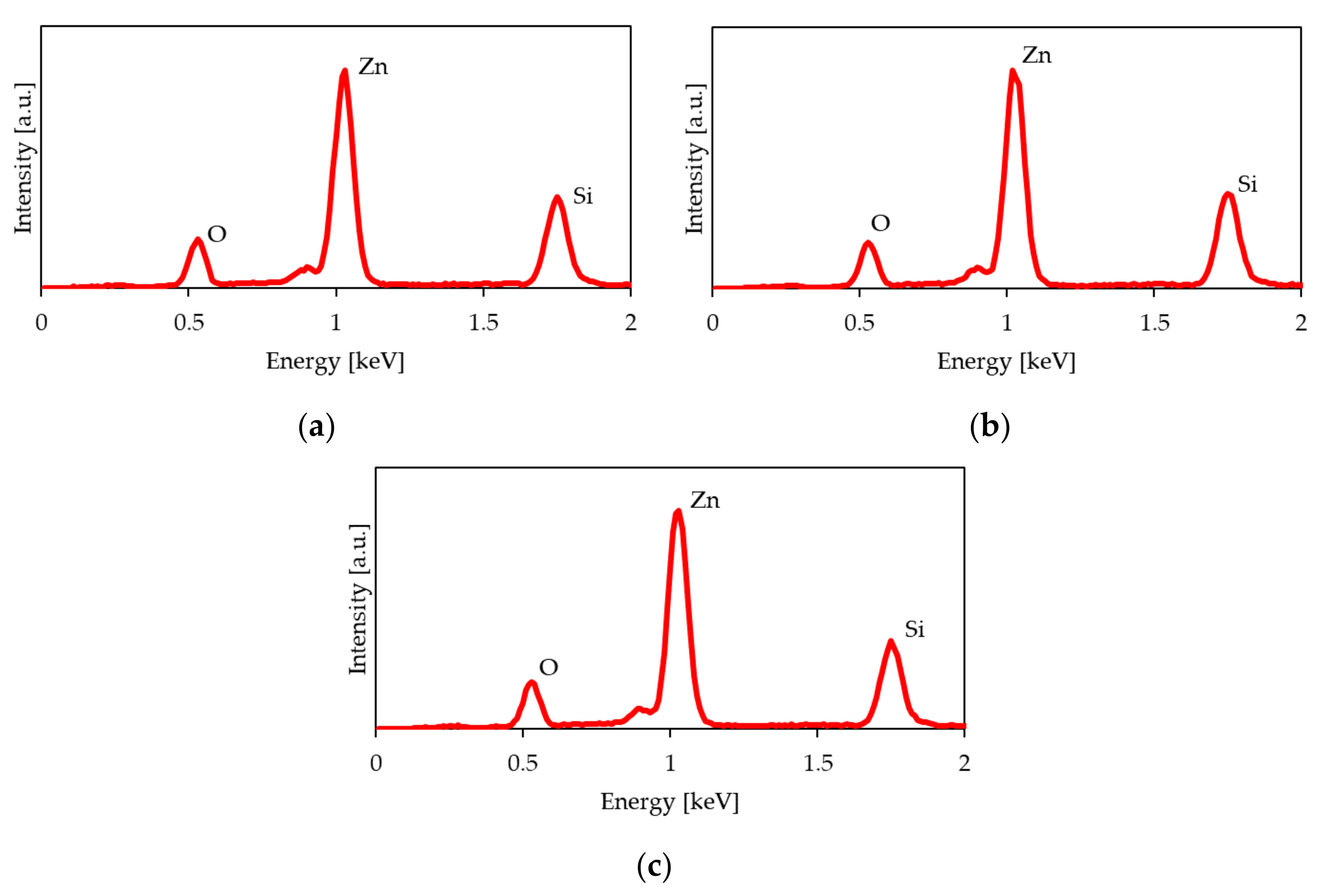
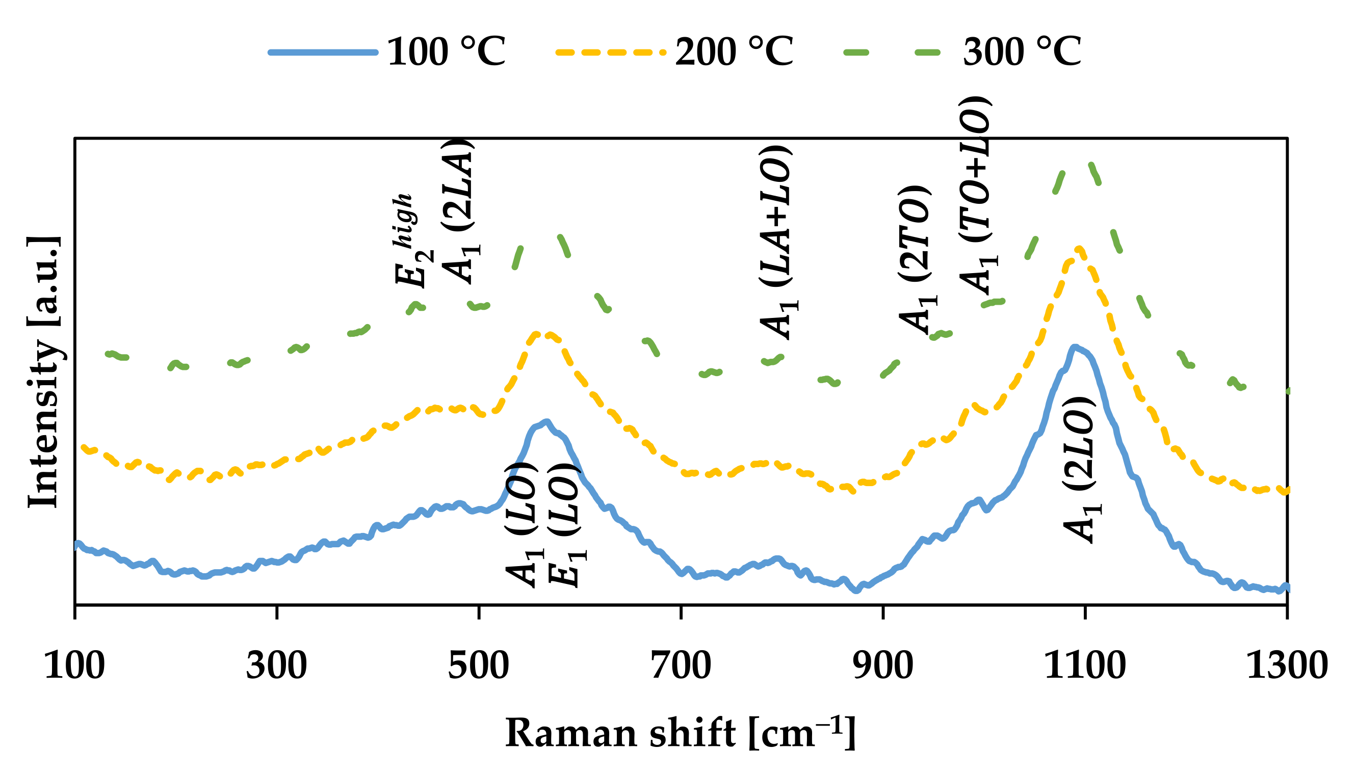
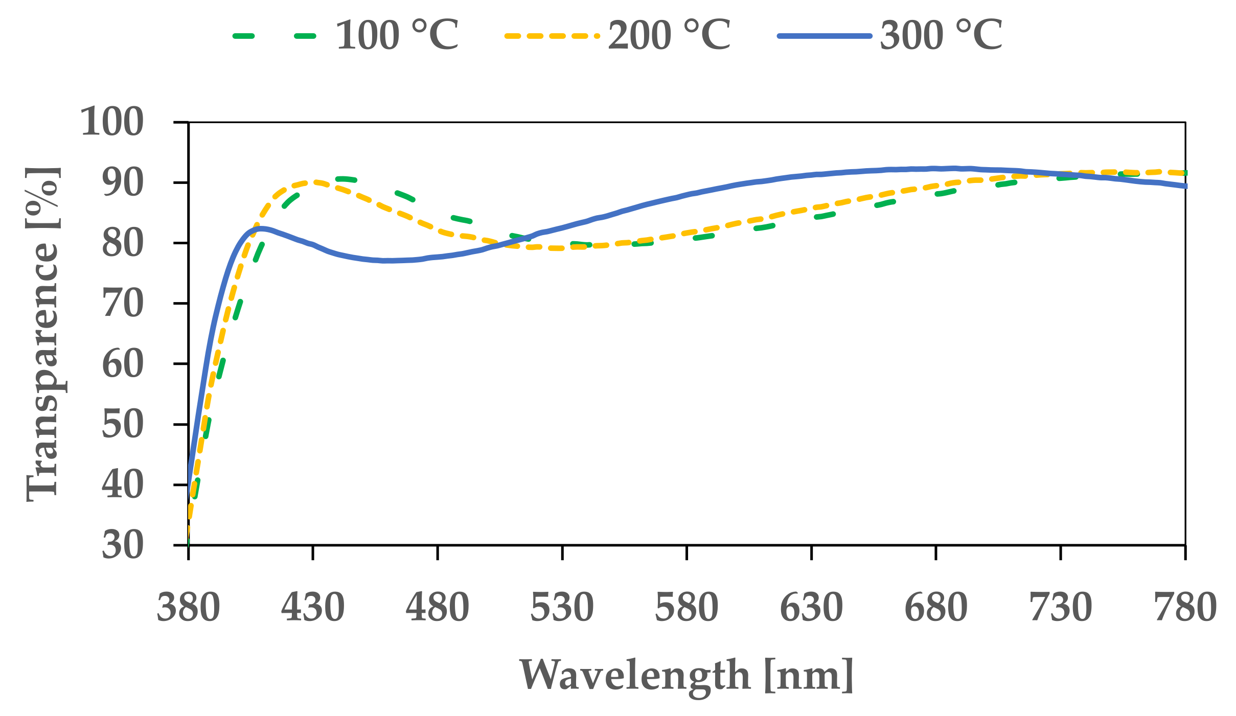
3. Results and Discussion
4. Conclusions
Author Contributions
Funding
Institutional Review Board Statement
Informed Consent Statement
Data Availability Statement
Conflicts of Interest
References
- Ali, H.M.; Mohamed, H.A.; Mohamed, S.H. Enhancement of the optical and electrical properties of ITO thin films deposited by electron beam evaporation technique. Eur. Phys. J. Appl. Phys. 2005, 31, 87–93. [Google Scholar] [CrossRef]
- Ellmer, K.; Andreas, K.; Bernd, R. Transparent Conductive Zinc Oxide. Basics and Applications in Thin Film Solar Cells; Springer: Berlin/Heidelberg, Germany, 2008. [Google Scholar]
- Hosono, H.; Ohta, H.; Orita, M.; Ueda, K.; Hirano, M. Frontier of transparent conductive oxide thin films. Vacuum 2002, 66, 419–425. [Google Scholar] [CrossRef]
- Stadlerh, A. Transparent conducting oxides—An up-to-date overview. Materials 2012, 5, 661–683. [Google Scholar] [CrossRef]
- Muchuweni, E.; Sathiaraj, T.S.; Nyakotyo, H. Synthesis and characterization of zinc oxide thin films for optoelectronic applications. Heliyon 2017, 3, e00285. [Google Scholar] [CrossRef] [Green Version]
- Ismail, A.; Abdullah, M.J. The structural and optical properties of ZnO thin films prepared at different RF sputtering power. J. King Saud Univ. Sci. 2013, 25, 209–215. [Google Scholar] [CrossRef] [Green Version]
- Faÿ, S.; Kroll, U.; Bucher, C.; Vallat-Sauvain, E.; Shah, A. Low pressure chemical vapour deposition of ZnO layers for thin-film solar cells: Temperature-induced morphological changes. Sol. Energy Mater. Sol. Cells 2005, 86, 385–397. [Google Scholar] [CrossRef] [Green Version]
- Silva, É.P.; Chaves, M.; Durrant, S.F.; Lisboa-Filho, P.N.; Bortoleto, J.R.R. Morphological and electrical evolution of ZnO:Al thin films deposited by RF magnetron sputtering onto glass substrates. Mater. Res. 2014, 17, 1384–1390. [Google Scholar] [CrossRef] [Green Version]
- Kim, S.; Yoon, H.; Kim, D.Y.; Kim, S.; Leem, J.Y. Optical properties and electrical resistivity of boron-doped ZnO thin films grown by sol–gel dip-coating method. Opt. Mater. 2013, 35, 2418–2424. [Google Scholar] [CrossRef]
- Smirnov, M.; Baban, C.; Rusu, G.I. Structural and optical characteristics of spin-coated ZnO thin films. Appl. Surf. Sci. 2010, 256, 2405–2408. [Google Scholar] [CrossRef]
- Wenas, W.W.; Yamada, A.; Takahashi, K. Electrical and optical properties of boron-doped ZnO thin films for solar cells grown by metalorganic chemical vapor deposition. J. Appl. Phys. 1991, 70, 7119–7123. [Google Scholar] [CrossRef]
- Kumar, G.; Kumar, R.; Kumar, A. ZnO thin films: Chemical vapour deposition, growth and functional properties. Rev. Adv. Sci. Eng. 2016, 5, 150–160. [Google Scholar] [CrossRef]
- Lontino Fomekong, R.; Saruhan, B. Influence of humidity on NO2-sensing and selectivity of spray-CVD grown ZnO thin film above 400 °C. Chemosensors 2019, 7, 42. [Google Scholar] [CrossRef] [Green Version]
- Petrella, A.J.; Deng, H.; Roberts, N.K.; Lamb, R.N. Single-source chemical vapor deposition growth of ZnO thin films using Zn4O(CO2NEt2)6. Chem. Mater. 2002, 14, 4339–4342. [Google Scholar] [CrossRef]
- Hamelmann, F.U. Thin film zinc oxide deposited by CVD and PVD. J. Phys. Conf. Ser. 2016, 764, 012001. [Google Scholar] [CrossRef] [Green Version]
- Fouad, O.A.; Ismail, A.A.; Zaki, Z.I.; Mohamed, R.M. Zinc oxide thin films prepared by thermal evaporation deposition and its photocatalytic activity. Appl. Catal. B Environ. 2006, 62, 144–149. [Google Scholar] [CrossRef]
- Bensmaine, S.; Benyoucef, B. Effect of the temperature on ZnO thin films deposited by r.f. magnetron. Phys. Procedia 2014, 55, 144–149. [Google Scholar] [CrossRef] [Green Version]
- Jimenez-Cadena, G.; Comini, E.; Ferroni, M.; Vomiero, A.; Sberveglieri, G. Synthesis of different ZnO nanostructures by modified PVD process and potential use for 1dye-sensitized solar cells. Mater. Chem. Phys. 2010, 124, 694–698. [Google Scholar] [CrossRef] [Green Version]
- Wu, H.W.; Yang, R.Y.; Hsiung, C.M.; Chu, C.H. Characterization of aluminum-doped zinc oxide thin films by RF magnetron sputtering at different substrate temperature and sputtering power. J. Mater. Sci. Mater. Electron. 2013, 41, 166–171. [Google Scholar] [CrossRef]
- Muchuweni, E.; Sathiaraj, T.S.; Nyakotyo, H. Physical properties of gallium and aluminium co-doped zinc oxide thin films deposited at different radio frequency magnetron sputtering power. Ceram. Int. 2016, 42, 17706–17710. [Google Scholar] [CrossRef]
- Assunção, V.; Fortunato, E.; Marques, A.; Águas, H.; Ferreira, I.; Costab, M.E.V.; Martins, R. Influence of the deposition pressure on the properties of transparent and conductive ZnO:Ga thin-film produced by r.f. sputtering at room temperature. Thin Solid Films 2003, 427, 401–405. [Google Scholar] [CrossRef]
- Boryło, P.; Matus, K.; Lukaszkowicz, K.; Kubacki, J.; Balin, K.; Basiaga, M.; Szindler, M.; Mikuła, J. The influence of atomic layer deposition proces temperaturę on ZnO. Appl. Surf. Sci. 2019, 474, 177–186. [Google Scholar] [CrossRef]
- Cuscó, R.; Alarcón-Lladó, E.; Ibáñez, J.; Artús, L.; Jiménez, J.; Wang, B.; Callahan, M.J. Temperature dependence of Raman scattering in ZnO. Phys. Rev. B 2007, 75, 165202. [Google Scholar] [CrossRef]
- Thangavel, R.; Moirangthem, R.S.; Lee, W.S.; Chang, Y.C.; Weia, P.K.; Kumar, J. Cesium doped and undoped ZnO nanocrystalline thin films: A comparative study of structural and micro-Raman investigation of optical phonons. J. Raman Spectrosc. 2010, 41, 1594–1600. [Google Scholar] [CrossRef]
- Jothilakshmi, R.; Ramakrishnan, V.; Thangavel, R.; Kumar, J.; Saruac, A.; Kuball, M. Micro-Raman scattering spectroscopy study of Li-doped and undoped ZnO needle crystals. J. Raman Spectrosc. 2009, 40, 556–561. [Google Scholar] [CrossRef]
- Paul, S.; Harris, P.G.; Pal, C.; Sharma, A.K.; Ray, A.K. Low cost zinc oxide for memristors with high On–Off ratios. Mater. Lett. 2014, 130, 40–42. [Google Scholar] [CrossRef]
- Cho, S. Effects of growth temperature on the properties of ZnO thin films grown by radio-frequency magnetron sputtering. Trans. Electr. Electron. Mater. 2009, 10, 185–188. [Google Scholar] [CrossRef] [Green Version]
- Yang, W.; Wang, F.; Guan, Z.; He, P.; Liu, Z.; Hu, L.; Chen, M.; Zhang, C.; He, X.; Fu, Y. Comparative study of ZnO thin grown on quartz glass and sapphire (001) substrates by means of magnetron sputtering and high-temperature annealing. Appl. Sci. 2019, 9, 4509. [Google Scholar] [CrossRef] [Green Version]
- Chaabouni, F.; Abaab, M.; Rezig, B. Effect of the substrate temperature on the properties of ZnO films grown by RF magnetron sputtering. Mater. Sci. Eng. B 2004, 109, 236–240. [Google Scholar] [CrossRef]


| Process Temperature | Spectroscopic Ellipsometry (nm) | Scanning Microscopy (nm) |
|---|---|---|
| 100 °C | 195 | 191 |
| 200 °C | 197 | 194 |
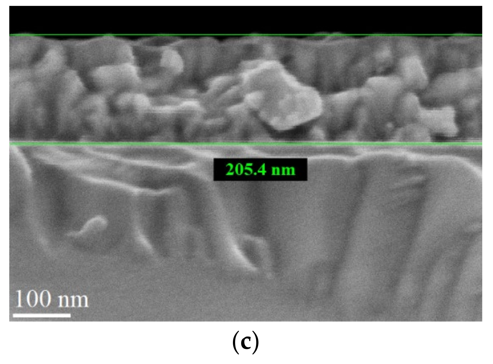
| 300 °C | 207 | 205 |
| Process Temperature | Rq (nm) | Ra (nm) |
|---|---|---|
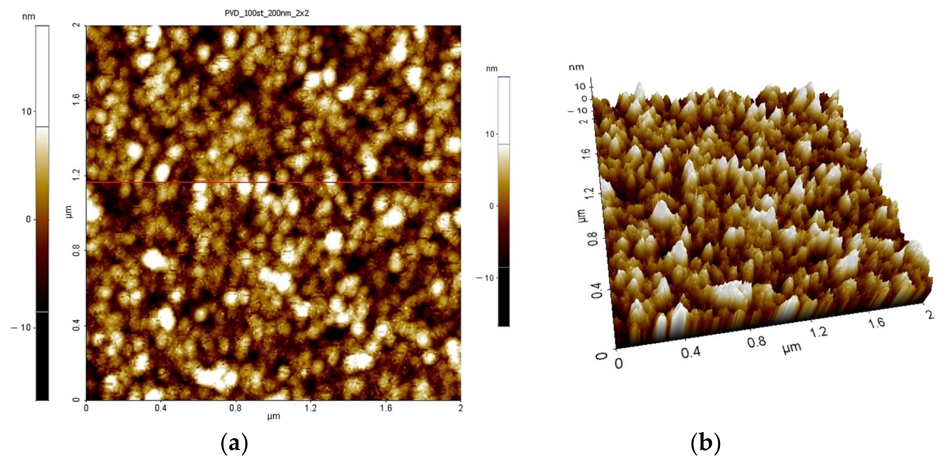
| 100 °C | 3.38 | 3.10 |
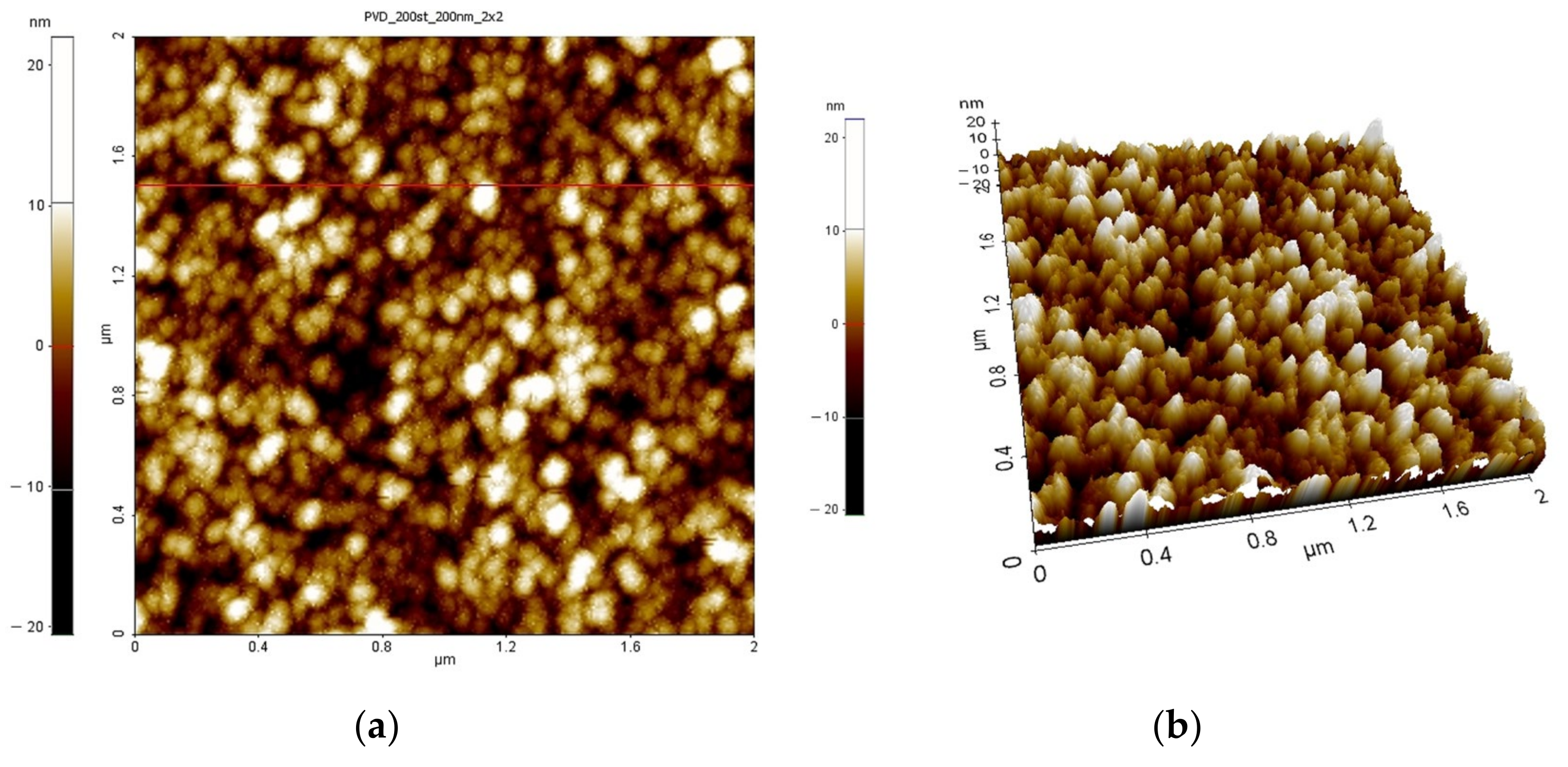
| 200 °C | 4.42 | 3.39 |
| 300 °C | 4.49 | 3.57 |
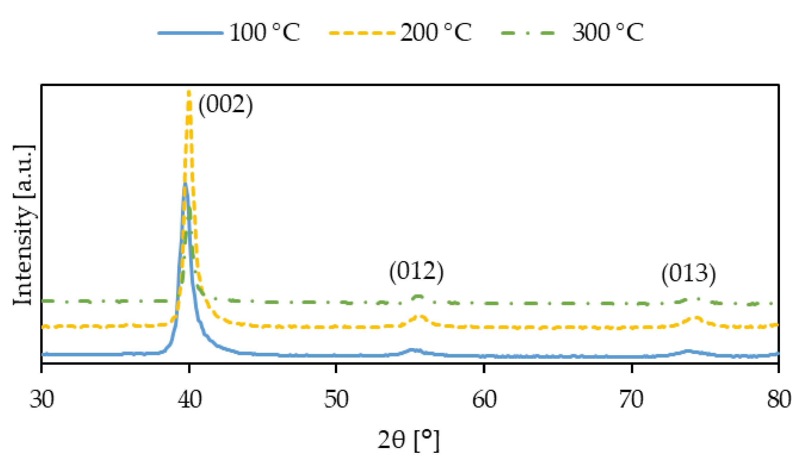
| Process Temperature | 2θ (°) | Crystallite Size, D (nm) |
|---|---|---|
| 100 °C | 39.75 | 49 |
| 200 °C | 39.95 | 51 |
| 300 °C | 39.95 | 62 |
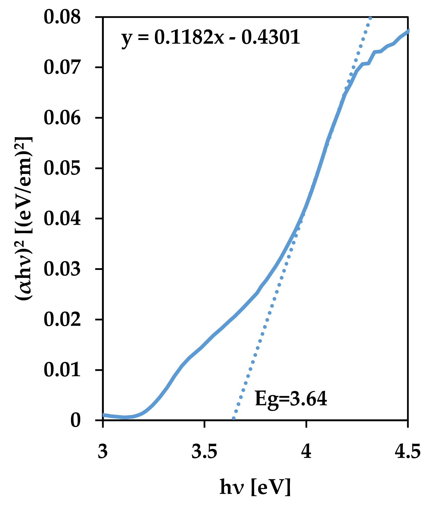
| Process Temperature | Optical Energy Bandgap, Eg (eV) |
|---|---|
| 100 °C | 3.64 |
| 200 °C | 3.62 |
| 300 °C | 3.56 |
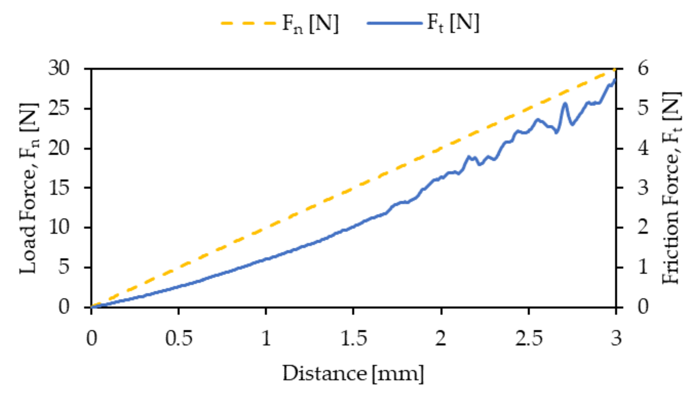
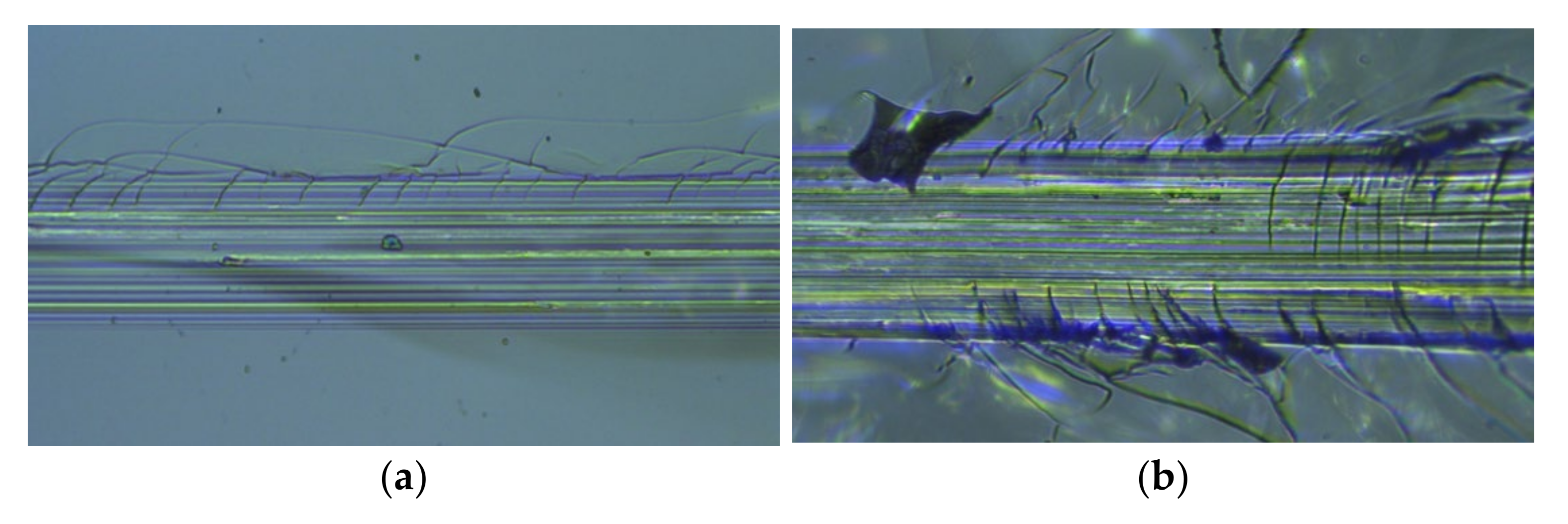
| Process Temperature | Critical Load LC1 (N) | Critical Load LC2 (N) |
|---|---|---|
| 100 °C | 3.7 | 17.7 |
| 200 °C | 7.4 | 22.6 |
| 300 °C | 16.6 | 26.1 |
Publisher’s Note: MDPI stays neutral with regard to jurisdictional claims in published maps and institutional affiliations. |
© 2021 by the authors. Licensee MDPI, Basel, Switzerland. This article is an open access article distributed under the terms and conditions of the Creative Commons Attribution (CC BY) license (https://creativecommons.org/licenses/by/4.0/).
Share and Cite
Kaim, P.; Lukaszkowicz, K.; Szindler, M.; Szindler, M.M.; Basiaga, M.; Hajduk, B. The Influence of Magnetron Sputtering Process Temperature on ZnO Thin-Film Properties. Coatings 2021, 11, 1507. https://doi.org/10.3390/coatings11121507
Kaim P, Lukaszkowicz K, Szindler M, Szindler MM, Basiaga M, Hajduk B. The Influence of Magnetron Sputtering Process Temperature on ZnO Thin-Film Properties. Coatings. 2021; 11(12):1507. https://doi.org/10.3390/coatings11121507
Chicago/Turabian StyleKaim, Paulina, Krzysztof Lukaszkowicz, Marek Szindler, Magdalena M. Szindler, Marcin Basiaga, and Barbara Hajduk. 2021. "The Influence of Magnetron Sputtering Process Temperature on ZnO Thin-Film Properties" Coatings 11, no. 12: 1507. https://doi.org/10.3390/coatings11121507