Article

Sputter Deposited Metal Layers Embedded in Composites—From Fundamentals to Applications

1
Department of Materials, Textiles and Chemical Engineering, Faculty of Engineering and Architecture, Ghent University, Technologiepark Zwijnaarde 46, B-9052 Zwijnaarde, Belgium
2
Department of Solid State Sciences, Ghent University Krijgslaan 281(S1), B-9000 Gent, Belgium
*
Author to whom correspondence should be addressed.
Coatings 2021, 11(2), 190; https://doi.org/10.3390/coatings11020190
Submission received: 6 January 2021 / Revised: 22 January 2021 / Accepted: 27 January 2021 / Published: 6 February 2021
(This article belongs to the Section Thin Films)

Abstract

:
Due to the low heat flux towards the substrate, magnetron sputter deposition offers the possibility to deposit thin films on heat sensitive materials such as fiber-reinforced polymers, also known as composite materials. Passive thermal probe measurements during the sputter deposition of metal layers show indeed that the temperature increase remains well below 25 °C for film thicknesses up to 600 nm. The latter thickness threshold is based on the influence of embedded metal films on the adhesion of the composite plies. Films thicker than this threshold deteriorate the mechanical integrity of the composite. The introduction of the uncured composite in the vacuum chamber strongly affects the base pressure by outgassing of impurities from the composite. The impurities affect the film properties as illustrated by their impact on the Seebeck coefficient of sputter deposited thermocouples. The restrictions to embed thin films in composites, as illustrated by both the heat flux measurements, and the study on the influence of impurities, are however not insurmountable. The possibility to use embedded thin films will be briefly demonstrated in different applications such as digital volume image correlation, thermocouples, and de-icing.

1. Introduction

Nowadays, the term composite material is mostly used to refer to fiber-reinforced polymers (FRPs). The most commonly used types of fibers are carbon, glass or aramid fibers, but also silicon carbide or inorganic oxide fibers (alumina/silica) can be encountered. Different fabrication procedures for the production of polymer composites are available. One of the approaches uses prepregs plies, that is, sheets of fibres pre-impregnated with partially cured resin. The plies of prepreg are stacked into a laminate. This stack is then consolidated into a single piece by applying heat, often assisted by an over-pressure environment which compacts the composite laminate and disables the formation of voids and bubbles in the resin. Over the years, FRPs have taken a strong position as a material choice for advanced applications and all-day use. FRPs are composite materials and exhibit some unique properties such as very high specific stiffness and strength, good fatigue durability, and good resistance against corrosion. Compared to metals, composites are an interesting alternative material choice with regard to weight savings, for example, for fuel efficiency in transport and aerospace industry. The Boeing 787 Dreamliner or Airbus A350 are passenger airliners for which the primary structure is composed—in addition to the more common materials such as titanium, aluminum and steel—for 50% out of FRPs [1,2]. Other examples are the use of composite materials for sports equipment such as lightweight racing bikes or tennis rackets, or for big engineering structures such as bridge decks [3] or wind turbine blades [4,5,6]. However, during both the production cycle and the exposure to impact and fatigue while in service, composite materials are prone to defects and internal damage. Of course, with the cost of material failure within these big and critical structures being unacceptably high, the widespread use of composite materials has pushed the demand for monitoring the production cycle, the structural health, and the environmental conditions during operation. Nowadays, sensors are used to monitor the curing cycle in the autoclave, or the environmental conditions during operation such as temperature, humidity, or mechanical strain. Some examples of embedded sensor approaches are optical fibers with Bragg gratings [7,8,9,10], polymer waveguides [11] to measure strain and temperature, piezoelectric sensor networks [12,13] or capacitive sensors [14] to monitor the dielectric properties of the polymer matrix during curing. A major constraint is that the embedded sensor can only add value or functionality, but cannot compromise on the structural properties of the host material. Therefore, it is necessary for the sensors to have restricted out-of-plane dimensions in order not to deteriorate the material structure [10]. As the individual composite plies have thicknesses of 120–150 micron (autoclave prepreg’s) up till 500–1000 micron (for heavy textiles and 3D woven fabrics), thin films of a few 100 nanometers have the potential to address this constraint. Furthermore, as illustrated by some examples in this paper, (see Section 3.4), the use of embedded thin films in composite materials is accompanied by a range of possible applications.
Magnetron sputtering is widely used deposition technique. It benefits from its relatively low heat flux towards the substrate enabling deposition on plastic foils, and on other heat sensitive substrates. Moreover, the transfer from laboratory results to industrial applications is rather straightforward because magnetron sources can easily be upscaled. Depositions are performed however in a high vacuum chamber which sets some requirements to materials used within the deposition environment, including the substrate. Strongly outgassing substrates should be avoided and/or treated with special care. For example, in roll-to-roll coaters the (un)winding of the foil is typically performed in an extra vacuum chamber only connected to the deposition chamber via a narrow gap to avoid unwanted species to enter the deposition chamber. It is well known that impurities can affect the film microstructure/texture, and hence the envisaged film properties. To embed thin films in the FRP or composite, the sputter deposition must occur on a prepreg ply which will degas in the vacuum system. This can induce curing but will also affect the impurity content in the deposited thin film. The effect of both processes can be reduced by a shorter deposition time, or stated differently by a high deposition rate. The required higher discharge power will however increase the heat flux towards the substrate causing melting (for thermoplastics) or curing (for thermosets) of the prepreg ply. In this work, the boundary conditions for sputter deposition on composites are investigated. First, the impact of the embedded thin film on the mechanical strength of the composite is studied (see Section 3.1). In Section 3.2, the temperature increase of the sample as function of time is estimated based on a measurement of the heat capacity of the used composite material, and the heat flux towards the sample. The measurement of the impurities, and their influence on some film properties is presented Section 3.3. Finally, some possible applications such as embedded thermocouples, digital volume correlation and deicing are discussed in Section 3.4.

2. Experimental

Composite laminates were produced from MTC275 out-of-autoclave glass fiber based prepreg plies (Castro Composites). All laminates were produced by a unidirectional lay-up of 32 plies of prepreg where the treated prepreg plies occupy the midplane. The recommended temperature cycle for curing is given by a dwell step at 85 °C for 2 ± 0.5 h reached at a ramp rate of 1 °C per minute, followed by 1 h at 130 °C reached at a ramp rate of 2 °C per minute.
The impact of the embedded thin films on the mechanical properties of the laminate was evaluated based on the ASTM D2344 standardized test [15]. The choice for this test is based on the fact that the films are deposited at the interface between neighboring plies. Hence, it can be expected that mainly the interfacial adhesion between the composite layers will be affected. Indeed, the test, known as the short-beam shear test, is a bending test with a strongly reduced span. In such a way, the transverse shear stresses become much more important, compared to the bending stresses. This test is commonly used to characterize the quality of the interfaces between the different layers of a composite, because the shear stress between the different layers might lead to delamination or decohesion. Following the described procedure, a short beam with dimensions of 12 mm × 32 mm × 6 mm was placed on two supports that allow lateral motion. The span length was set at 24 mm. The laminate specimen is oriented with the fiber direction in the span direction, and is center-loaded until fracture occurs.
Depositions were performed in a stainless steel cuboid vacuum chamber with a volume of 0.259 m3, pumped by a combination of rotary and turbomolecular pump. The residual gas pressure was below 4 × 10 4 Pa as measured with CompactFullrange Gauge (Pfeiffer Vacuum, PKR 251). The sputter gas pressure was measured by means of a capacitance gauge (Pfeiffer Vacuum, CMR 274). The depositions were performed in a pressure range between 0.3 to 1.2 Pa. Two inch diameter circular targets were mounted on a home-built magnetron powered by a DC power supply operating in constant current mode (Hüttinger 1500 DC). Deposition were performed on three different types of substrates. Depositions for thin film analysis are typically performed on silicon cleaned occording the RCA (Radio Corporation of American) procedure. For the electrical characterization, that is, film resistivity and thermoelectric properties, deposition is performed on glass substrates. Finally, the aforementioned prepreg plies were also used as substrate. The procedure to deposit thermocouples is described in [16].
The energy flux towards the substrate during the DC magnetron sputtering process was measured using a calorimetric probe [17]. This probe consists of a K-type thermocouple welded on the back of a sensing element with a diameter of 10 mm. The heat capacity of the sensor was 0.048 J/K. The output of the calorimetric probe is connected to the computer through a data-acquisition unit (National Instruments) and a software package determines the energy flux towards the substrate by fitting the heating and cooling temperature curves with the Levenberg-Marquardt algorithm. The probe was installed in front of the cathode surface and energy fluxes were measured for different deposition conditions. The standard deviation on the measurements is 1 mW/cm 2 .
Differential scanning calorimetry (DSC1/700, Mettler-Toledo) was performed to determine temperature dependence of the heat capacity of uncured (carbon/expoxy) prepreg material.
The deposition rate, and the atomic flux towards the substrate, are calculated from the film thickness, the deposition time, and the film density. The film thickness was measured by means of contact profilometry (Talystep Taylor-Hobson). The profilometry is performed on a partially coated (RCA cleaned) silicon substrate. The step between the coated and the uncoated substrate is measured by the profilometer tip and determines the thickness of the layer. The thickness was always measured at four different steps on the sample and afterwards the different measurements are averaged. The standard deviation on the thickness measurements is around 30 nm. In order to measure the density, X-ray reflectivity (XRR) was consulted on a Bruker D8 Advance with a scintillation detector and CuK α radiation. The density could be determined based on the critical angle seen from the obtained pattern, taking into account the chemical composition of the samples.
The outgassing of prepreg plies in the vacuum chamber was studied using a quadrupole mass spectrometer (Hiden Analytical, EQP 1000) with an orifice of 300 μ m in residual gas analysis mode.
In the context of the deicing application, infrared inspection of the surface of the studied composites was performed by mean of a high-end thermographic camera (FLIRA6750sc). A black spray coating was therefore applied onto the surface in order to set the emissivity of the surface close to one.

3. Results and Discussion

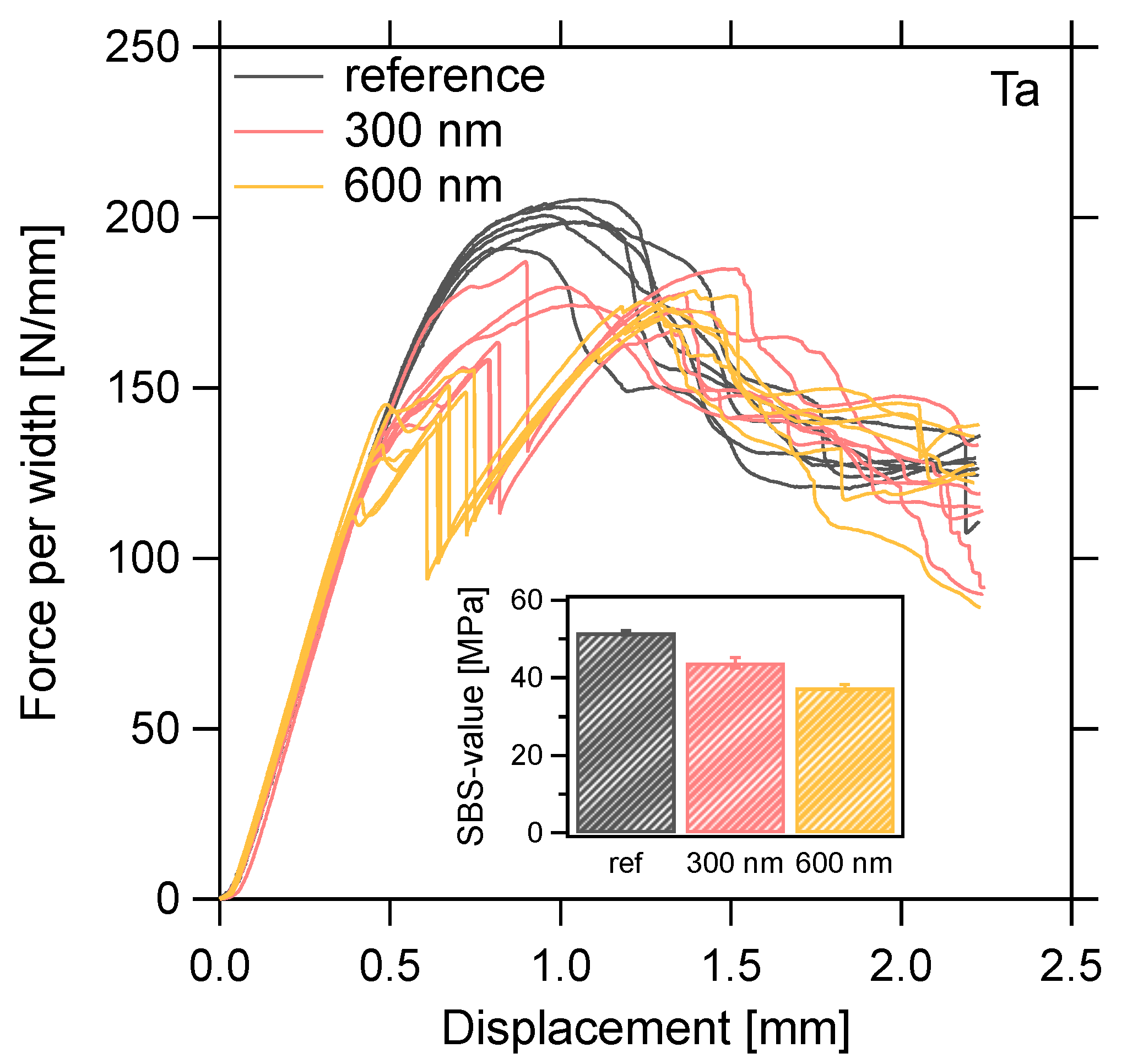
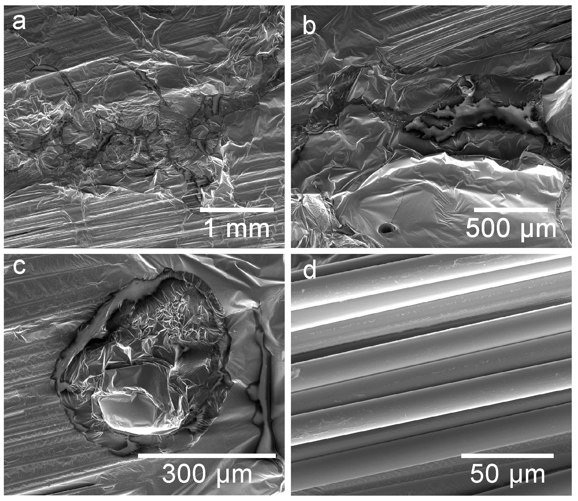
3.1. Mechanical Strength

For a first series of experiments, four unidirectional laminates are produced with different conditions for the mid-plane prepreg ply (Figure 1): a reference ply, a fully coated prepreg ply, a prepreg ply coated with lines of 2 mm width, and a prepreg ply without any deposition but with an exposure to vacuum for the same amount of time as the coated samples, that is, 300 s pre-vacuum at ∼1 Pa and 210 s in a high vacuum at ∼4 × 10 4 Pa. The applied coatings were 150 ± 30 nm thick sputter-deposited constantan (Cu 55 Ni 45 ) films. From the different laminates, representative samples were cut. The short-beam shear test, as prescribed by the standard [15], requires a span-to-thickness ratio of 4, and test specimens with a length of 6 × thickness and a width of 2 × thickness. With the thickness of the laminates ∼6 mm, the span length was 24 mm and the dimensions of the specimens in our case were 12 mm × 36 mm. The coated surface area fractions within the test samples are 0, 100, 17, and 0% respectively.
An overview of all the results of the mechanical tests is presented in Figure 1. Each sample was tested multiple times to verify the reproducibility of the results. The behavior between the different samples is very comparable in the elastic regime. The onset for fracture however is different. The fracture load, interpreted as the first attained maximum load, is taken as a measure for the apparent shear strength of the material. The insert in Figure 1 compares the average short-beam-shear (SBS) strength values obtained for the reference, full area coated, the line patterned and the vacuum exposed samples are respectively given by 42.6 ± 0.3, 34.2 ± 0.1, 37.9 ± 1.0, and 39.6 ± 1.2 MPa. It is clear that there is an influence for both the presence of a coating on the prepreg as for the exposure of the prepreg to vacuum. The mechanical behavior and the SBS-values obtained for both the uncoated (vacuum exposed) sample and the sample with lines are however very comparable. This indicates that the exposure of the prepreg to the vacuum has a distinct influence on the SBS-value compared to the reference, but the influence of the limited surface coverage (∼17%) of the coating on the prepreg does not significantly affect the SBS-value.
A possible explanation for the reduced short-beam shear (SBS) strength after vacuum exposure is the reduced adhesion to other prepreg plies due to dehydration of the epoxy in vacuum. When we increase the surface coverage from 17% to 100%, the mechanical behavior is remarkably different. A relaxation occurs at around 75% of the SBS-value of the reference. This relaxation can be attributed to the onset of delamination under influence of interlaminar shear. Basically, after relaxation, the sample can be seen as two separate samples with only half the thickness placed on top of one another. The cross-sectional moment of inertia I of the beam-like specimen determines the resistance to displacement under influence of stress or torque, and depends on the laminate thickness h as I h 3 . As a delamination occurs in the midplane, the moment of inertia of the specimen is strongly affected and offers less resistance against deformation. This is marked by the sudden drop in the load-displacement curve.
To investigate the impact of the film thickness, a similar experiment as described above was performed for laminates produced by vacuum assisted resin transfer molding [18]. Three sets of laminates were tested, consisting of a layup of six unidirectional fiber mats impregnated in epoxy with different conditions for the fiber mat in the midplane—a reference set, a set with a 300 nm tantalum (Ta) film applied over the entire fiber-surface in the midplane, and a set with a 600 nm tantalum (Ta) film, also applied over the entire fiber-surface in the midplane. The results are presented in Figure 2 and the obtained SBS-values are respectively given by 51.6 ± 0.5, 43.9 ± 1.3, and 37.4 ± 0.8 MPa. The failure behavior of the samples with the fully coated fibers is very similar to the behavior of the samples discussed in Figure 1 with the fully coated prepreg surface, indicating failure due to the formation of a delamination in the midplane. The samples however show a remarkable post-critical strength recovery as the sustained load increases above the fracture load. The decrease in SBS-value for the samples with increased layer thickness can probably be related to the decreased interdiffusion of the epoxy through porosities in the coating causing a restricted adhesion.
Based on the two series of experiments, it is possible to conclude that the impact of the embedded films remains limited, especially in the elastic regime and that the embedded thin films do not to compromise the structural integrity of the host material under typical loads. Possible effects can however not be excluded at more extreme loadings. Moreover, the structural integrity is not solely defined by the static interlaminar shear strength. Further research will be needed to evaluate the influence of the thin film deposition under for example dynamic loading conditions.

3.2. Heat Capacity and Heat Flux Measurements
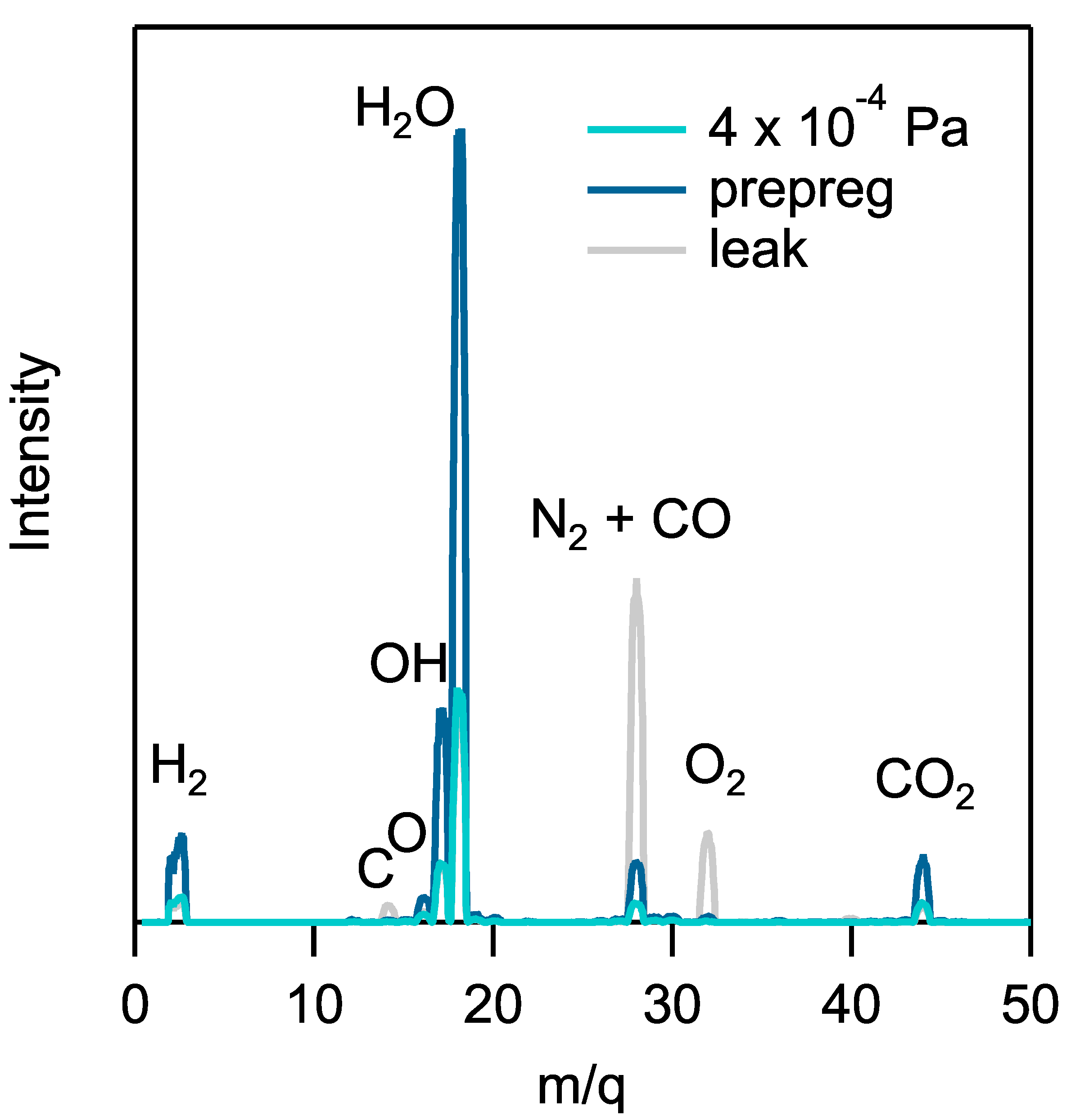
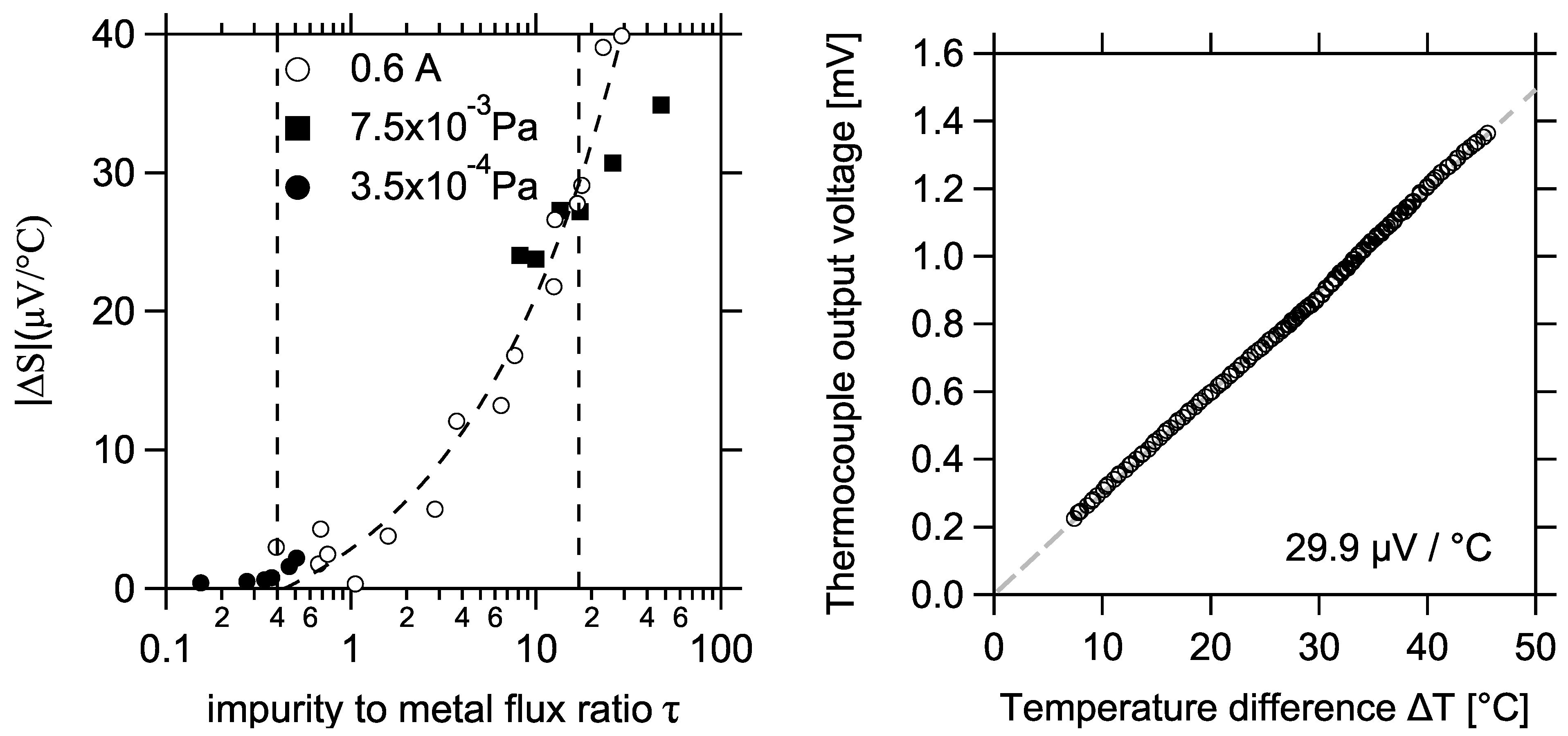
A too high heat load towards the composite prepreg substrate during deposition can cause local curing or deteriorate the adhesion between prepreg sheets in a laminate. This introduces weak spots in the laminate which are prone to delamination. As the impact of the deposition on the structural properties of the laminate must be limited as much as possible, it is important to study the heat flux during sputter deposition in order to control the heat load towards the substrate.
The results of the heat flux measurements are presented in Figure 3 (left) during the deposition of chromel (Ni90Cr10) and constantan (Cu55Cr45). When the discharge current is doubled, the energy flux or dissipated power at the substrate is in good approximation doubled. We can understand this behavior based on the description of the IV-characteristic for a magnetron discharge. The IV-curve is steep and therefore when the current is doubled, the discharge voltage only varies over a small amount. As an example, for a given argon pressure of 0.3 Pa and a target-to-substrate of 10 cm, the discharge voltage varied respectively from 392 V to 416 V in the case of chromel and from 396 V to 419 V in the case of constantan, when the discharge current was varied from 0.3 A to 0.6 A. From this, we calculate the variation in dissipated power from 118 W to 250 W for chromel and from 119 W to 251 W for constantan. This calculation confirms that the dissipated power in the vacuum system approximately doubles when the discharge current is doubled. Therefore, also the power density, or energy flux, at the substrate will be doubled. Also the target-to-substrate distance has a clear influence on the energy flux. For a target-to-substrate distance varying over a factor three, that is, from 5 cm to 15 cm, the energy flux measured at a discharge current of 0.3 A almost decreased over an order of magnitude, that is, from approximately 100 mW/cm2 to 10 mW/cm2 and in the range of 200 mW/cm2 to 20 mW/cm2 at a discharge current of 0.6 A. This strong effect of the target-to-substrate distance on the energy flux is expected as on the one hand, the target-to-substrate distance plays a role in the thermalization process and on the other hand, the dissipated energy originating from the vicinity of the target surface is distributed over the solid-angle for which the area holds a quadratic relationship to the distance from the target (see Figure 3 (right)). This quadratic relationship with the target-to-substrate distance can—by approximation—be found in the data. Within our experimental range, the influence of the argon pressure on the overall energy flux is small. For an argon pressure varied over a factor three, that is, from 0.3 Pa to 0.9 Pa, the total energy flux decreased maximally by 25 percent for the largest pressure-distance product, P × d , combinations. The inconclusive trend of P × d on the total energy flux results from the fact that P × d only affects a fraction of the total energy flux, that is, the energetic contributions related to massive particles. In order to properly understand the film density, it is essential to disentangle energy effects and effects related to momentum transfer [19].
Figure 3 (right) represent the sputtered particle flux as function of the target-to-substrate distance, the argon pressure and the discharge current. The dependencies of the sputtered particle flux on the process conditions are very similar to the case of the energy flux discussed above. Doubling the discharge current doubles the amount of ionic bombardment events per second on the target. The associated change in discharge voltage is limited because of the steep IV-curve. As the sputter yield Y depends in good approximation linearly on the discharge voltage in a restricted voltage range [20,21,22], only a small variation in sputter yield is expected when the discharge current is doubled. Therefore, at doubled discharge current, the rate of particles ejected from the target is in good approximation also doubled. The particles are ejected from the target surface according to a (under-)cosine distribution. If there were no gas atoms present, the particle density in a given direction θ at a distance r from the (center) of the target surface would approximately be ∼ c o s ( θ ) / r 2 . Again, this quadratic relation with the distance from the origin is approximately found in the experimental data. Due to collision events with the atoms of the sputter gas during transport of the sputtered atoms towards the substrate, the initial angular distribution of the sputtered particles evolves towards a more uniform angular distribution of the particles arriving at the substrate. Within our experimental range, however, the observed effect of the argon pressure on the deposition rate is small. When the pressure is increased over a factor 3, from 0.3 Pa to 0.9 Pa, the material flux decreases at maximum by 15% again for the largest P × d -value, whereas an increase of the target-to-substrate distance over a factor 3, from 5 cm to 15 cm, approximately decreases the arriving material flux by an order of magnitude, that is, 90%.
The DSC measurements on the studied prepreg plies show that, in the range between 10 °C and 70 °C, the behavior of the heat capacity at constant pressure C p as a function of temperature is linear,
C p T = 4.53 ± 0.03 × 10 3 T + 0.866 ± 0.001
with an R-square value of 0.998. The glass transition temperature equaled 117.6 °C (onset temperature: 112.5 °C). Similar values and behavior have been reported by Kalogiannakis et al. [23].
With the knowledge of the heat capacity of the prepreg ply, the heat flux, and the deposition rate (Figure 3), an estimation of the total temperature increase on 1 cm thick sample for a deposition of a specified thickness can be given by
Δ T = F E v D ρ p p C p Δ T d ,
with F E the energy flux, v D the deposition rate, ρ p p the density of the carbon/epoxy prepreg, C p , the temperature dependent heat capacity as determined by DSC, and d the film thickness. The density of the carbon prepreg was calculated as 1.6 g/cm 3 for a fiber-to-volume fraction of 65%, with values for the density of 1.8 g/cm 3 for the carbon fiber and 1.2 g/cm 3 for the epoxy matrix. The calculated temperature increase is an estimate because in reality the sample is thinner, leading to a higher temperature, but it is placed on a stainless steel holder with a much larger mass acting as a heat sink. The calculated temperature increase Δ T as function of the layer thickness d is shown in Figure 4.
Both the heat load towards the substrate during deposition, and the mechanical properties of the final composite are affected by the film thickness. It is thus of importance to restrict the film thickness as much as possible. However, as will be discussed in Section 3.4, decreasing the overall layer thickness comes at a cost of deteriorated (thermo-)electrical film properties. Determining the optimal layer thickness requires a compromise between a restricted heat load and good film properties. Anticipating the results, once the layer thickness exceeds 100 nm, a more bulk-like behavior of the film is observed. Therefore, at least a 100 nm film is required if no compromise on film properties is allowed. An additional constraint to be considered is related to the intrinsic roughness of an (uncured) prepreg surface due to the presence of both fibers and the resin. Scanning electron microscopy (SEM) images of coated uncured prepregs shows a high degree of macroscopic surface roughness of the prepreg substrate as can be observed in Figure 5. When deposited on such a rough surface, a too thin film risks to be discontinuous. Of course, this is detrimental when aiming for electrical applications. Furthermore, as the mobility of the polymer chains increases with temperature, local displacement of the epoxy is observed which can also deteriorate the continuity of the film. Moreover, the probability for a breakage of the film pattern decreases with an increasing film thickness. Studies on the strain-to-rupture show indeed that thicker thin film can withstand larger strains [24]. Values for the strain-to-rupture larger than 20% are reported for film thicker than 200 nm. Hence, from the perspective of film continuity and stability, somewhat thicker films are thus preferred. Based on the DSC-measurements, it is necessary to prevent the substrate temperature to exceed 70 C in order not to induce any phase transitions. If we preventively restrict the calculated temperature of the substrate by 20 degrees underneath the temperature barrier for a phase transition, a maximum temperature increase of 28 C is allowed (room temperature ≈ 22 C). This upper limit has no scientific ground, but is rather based on the practical experience obtained during this work. The constraints discussed above, are presented as colored areas on Figure 4. As such, a region appears which fulfills all constraints and where deposition is allowed without affecting the mechanical properties of the composite, the properties of the film, or risking breaking of the film pattern. The preferential region in which depositions are mostly performed in this work is indicated by the green box.

3.3. Impurities

Figure 6 show the residual gas analysis for three experimental conditions: the pumped high vacuum chamber (base pressure 4 × 10 4 Pa, the same vacuum chamber with a prepreg substrate introduced, and the vacuum chamber with an intentionally leak to the atmosphere. The presence of the five layer prepreg laminate substrate (6 × 27 × 0.1 cm3 into the vacuum chamber causes a strong increase of the water vapor into the vacuum chamber.
Although the prepreg was taken out of storage at −18 °C and left for over an hour to acclimatize, the water vapor is most likely the result of traces of condensation and adsorbed gases. Indeed, similar results are obtained in a study on the outgassing of cured (fiber-reinforced) epoxy resins in vacuum as measured by an electrobalance [25]. The latter study reports on a decreasing weight loss of the vacuum-exposed epoxy sample with time. A second vacuum exposure of the sample, after again nine days of exposure to the air, showed an identical weight loss, which indicates that the origin of the outgassing products are ad- or absorbed gases. Similar to our measurement presented in Figure 6, the outgassing products were identified by mass spectrometry measurements as mainly water vapor and small amounts of nitrogen, oxygen and carbon dioxide. H2O is the main source of the H2 and OH species present in the chamber [26,27,28]. The presence of these species during deposition will effectively influence the microstructure and film properties [28,29,30,31,32,33]. The role of impurities on the nucleation density during reactive magnetron sputtering was previously investigated by our team [34]. It was shown that the presence of O2, N2, or H2O species during deposition can severely affect thin film growth.
The impact of impurities on the film growth was evaluated from the impurity-to-metal impingement ratio τ , that is, the relative amount of impurities impinging on the surface per arriving adatom. It was shown that, in the low-impurity regime, that is, when τ < 1 , the domain size was not significantly or consistently affected by the presence of impinging impurities. This was understood as the spatial distribution between chemisorbed impurity species is larger than the characteristic length of the metal adatoms. For larger impurity-to-metal ratios, that is, τ > 1 , the spatial distribution between the chemisorbed species will be smaller than the characteristic length of the diffusing adatoms. In this case, the explored diffusion area of the adatom is restricted by the presence of different nucleation sites within this area, promoting nucleation and consequently grain-refinement. A power-law behavior D τ α is observed, which describes the decrease in domain size with increasing impurity-to-metal ratio τ for all materials studied in [34]. When the exponent α is averaged over the different materials, a value α = 0.50 ± 0.07 was found. This material-independent power-law behavior was also successfully simulated by means of a kinetic Monte Carlo code for a nucleation-dominated growth model. This power law behavior was also illustrated for the resistivity of constantan (Cu55Ni45 and chromel (Ni90Cr10) thin films [35]. The same behavior is observed for the Seebeck coefficient as shown in Figure 7 (left) [16].

3.4. Examples of Some Possible Applications

3.4.1. Single Alloy Embedded Thermocouple

Due to its simplicity, the structure of a thermocouple, that is, a couple of two dissimilar conductors, has remained unquestioned and invariant for a long time. More recently, Liu et al. [36] proposed a very simple, alternative approach for the production of thin film thermocouples (TFTCs) constituted out of the same material, that is, a single metal thermocouple. They demonstrated that the size-effect in metallic thin films can be exploited to fabricate TFTCs constituted of films of the same material, but with different thermoelectric properties. As such, a single-metal TFTC was constructed, composed of two sputter-deposited Ni thin films with different spatial dimensions and with sensitivities around 1 μ V/ C. Zhang et al. [37] also demonstrated that the thinner the films used in the TFTC, the faster the response time (≈52 ns). However, given the constraint on the layer thickness due to the intrinsic roughness of the prepreg substrate (see discussion related to Figure 4), the approach for the production of single-metal thermocouples based on the size-effect seems not applicable for the deposition on composites.
However, based on the results presented in Section 3.3, an alternative approach can be proposed. Indeed, the results summarized in Figure 7 shows that the film Seebeck coefficient deviates from its bulk value according to | Δ S | τ 1 / 2 . An increased impurity concentration present in the vacuum chamber during deposition can thus be used to tune the thermoelectric properties of the film. Or stated differently a single-metal TFTC can be created by combining two thermocouple legs of the same material, but with one leg deposited in the low-impurity regime, and another leg in the high-impurity regime. Figure 7 indicates that the presence of the composite in the vacuum is already a source of impurities itself. Therefore, whereas initially the outgassing related to the presence of the composite was considered as a negative situation, the usage of the high-impurity regime in the deposition process of a single-metal thermocouple allows for an opportunity to turn the outgassing into a useful tool for tuning film properties.
Following the deposition procedure described in [16] one thermocouple leg was deposited on a laminate stacking of 2 prepreg layers. The deposition was performed immediately after the introduction of the substrate in the vacuum chamber, that is, after 20 s after introduction. The deposition occurred at τ value of approximately 17. After the deposition of the first thermocouple leg, the system was given sufficient time to move into a low impurity regime. Here, at τ = 0.4, the second leg of the thermocouple, that is, again a 300 nm constantan film, is deposited. The expected sensitivity of the single metal thermocouple is given by the difference between the thermoelectric properties of the first thermocouple leg deposited in the high-impurity regime, and the second thermocouple leg deposition in the low impurity regime. From Figure 7 (left), the sensitivity of the single-alloy thermocouple is estimated as | Δ S | 27 μ V/ C. Figure 7 (right) shows the experimentally measured thermocouple output voltage as a function of the applied temperature difference. From the measurement, the sensitivity of the thermocouple is found to be 29.9 μ V/ C, which is very close to the predicted value of 27 μ V/ C. It is thus possible to fabricate single-metal thin film thermocouples by tuning the thermoelectric properties of the films by means of impurities. The obtained sensitivity is in the same range as the sensitivity of bulk K- and E-type thermocouples [38]. Single-metal TFTCs allow for a much simpler fabrication process compared to bimetallic thermocouples as only one magnetron source has to be used which is easier to control the process and reduces the production costs.

3.4.2. Deicing

Ice formation on a plane during flight causes an increased weight and drag and decreases the lift of the plane. Many accidents with airplanes could be attributed to effects directly or indirectly related to ice accumulation on the plane’s surfaces. The primary objective of anti-icing and de-icing is therefore to prevent or (periodically) remove accumulated ice formation on the plane surfaces. Icing may be categorized as light, moderate, and severe [39]. In severe icing conditions, the rate of formation (>4 cm per hour) is such that anti-icing and deicing may fail to control the ice accumulation. In moderate icing, the rate of ice formation (approximately 2 to 4 cm per hour) is such that there is potential for a hazardous situation. Light icing is usually not a problem unless the aircraft is exposed for a lengthy period (rate of ice formation approx. 0.1 to 2 cm per hour). Some common approaches for de-icing are either based on pneumatic boot systems, that is, a rubber membrane attached to the wing is inflated by means of compressed air in order to break the formed ice layer, on chemical fluids, or on electrical heating system (electro-thermal deicing).
For electro-thermal deicing applications on parts such as the airplane wings, it is not necessary to evaporate or to melt all of the impinging droplets on the surface. By periodic melting of the surface-air interface, typically with a power on-time of 9 s and an off-time of 3 min, the ice droplets no longer adhere to the surface and the accumulated ice is consequently removed by aerodynamic forces. In order to melt the ice, energy has to be supplied to heat the ice first to the zero point, and afterwards latent heat has to be applied to melt the ice. According the prescriptions of the Society of Automotive Engineers (SAE) standards AIR 1168/4 [40] the heating system must be able to deliver 34.10 kW/m 2 ), or 3.4 W/cm 2 .
Thin film heaters offer a light-weight advantage. Hence, a test is performed in order to evaluate if these prescribed power densities are feasible for thin film heaters.Experiments were first performed with thin film lines with a thickness of 100 nm as heating elements, but the main limitation of this approach are points of enhanced resistance in the heating element. These can originate from non-uniformities in the film thickness, but also due to the high surface roughness which can lead to discontinuities. As a consequence, these points limit the total current in the heating system, becomes a hot spot and is detrimental for the uniformity of the generated heat flux in the composite. Therefore, although it perhaps compromises on the structural integrity, a third test was performed with a fully coated (350 nm) prepreg ply as heating element, in order to reduce the impact of the points of enhanced resistance. The fully coated (350 nm) prepreg ply was integrated in the midplane of 10 layer laminate (approx. 30 cm 2 ). The film was all deposited under the following conditions: I = 0.6 A, P = 0.6 Pa, d T S = 10 cm, v d = 1 nm/s, and P B = 2 × 10 3 Pa. Copper was chosen as the deposited material because of the good electrical properties. A higher background pressure was however chosen in order to add some resistance to the heating circuit in order to prevent a short-circuit. After curing the samples, the contacting to the thin films was obstructed by a thin layer of epoxy. Copper tape was therefore applied onto the contact and perforated through the epoxy film in order to make electrical contact with the film. The power to the thin films was provided by means of a home-built DC voltage supply. The evolution of the surface temperature in case of a full coated heater ply is shown in Figure 8. It can indeed be observed that the surface temperature is rather homogeneously distributed. However, regions of elevated temperature are still observed at the ends of the electrode. A voltage of 40 V was applied over the 8.4 Ω heating film, resulting in a circuit current of 4.6 A. Consequently, the dissipated power by the heater is approximately 180 W, or expressed as a power density dissipated over the samples surface yields 5.9 W/cm 2 . The dissipated power density in this case, in contrast to the previous cases, clearly fulfills the requirements as outlined by the SAE standard (AIR 1168/4) [40]. Therefore, power densities in accordance to the prescription of the SAE standard (AIR 1168/4) [40] can indeed be dissipated by the thin film heating elements. Although these first results and numbers are thus in favor, currently the main challenges towards application are related to the homogeneity of the deposited film and the electrical contacting to the film. Contacting is a major obstacle for embedded applications in general [41,42,43,44,45]. In case of physical electrical contacting to the film, the film has to come out of the laminate stacking and needs to be exposed at the surface in one way or another. This creates film inhomogenities due to local pressure points during the curing process. As a consequence, this point limits the total current in the heating system, and becomes a hot spot which is detrimental for the uniformity of the generated heat flux in the composite. A much more convenient approach would be based on passive heating elements and a wireless power transfer through induction instead of physical contacting. In this case, the elements can be completely embedded in the composite which reduces the chances for the initiation of delamination and neutralizes the problem of the pressure points during curing. Further research on this inductive approach is performed and preliminary experiments demonstrate that film discontinuity is also no longer an obstacle for electrical heating as eddy currents can be generated within the film patches embedded in the composite.

3.4.3. Digital Volume Correlation

Digital image correlation (DIC) is a camera-based optical system, that, after calibration of the optical system, takes digital images of a reference pattern on the surface of the object. DIC permits to measure the in-plane and out-of-plane (using stereovision) deformation of a specimen surface under influence of an external load [46]. Subsequent spatial derivation of the measured deformation field yields the local strain field. When a random gray intensity distribution is present, the natural surface texture can simply be used as a reference pattern, but quite often a speckle pattern is applied on the surface. Even the feasibility of thin film patterns was already evaluated in this context [47]. DIC only allows to derive the strain at the surface but provides no information on the strain field components in the bulk of the material. For a better understanding of how damage forms and initiates in complex materials, information on the internal strain fields is required. Digital volumetric image correlation [48,49] (DVC) is a tomographic extension of DIC. X-ray micro-computed tomography is used to generate digital volume images of a sample. The material microstructure itself or internal markers such as the cross-sectional arrangement of the fibers, or pores within the sample can be used to provide a unique reference subset [50]. However, the visualization of the internal structure with X-ray micro-computed tomography (CT) suffers from poor contrast [18], and the less artifacts present in the composite, the more challenging it becomes to obtain a reference subset sufficient in size and contrast. Furthermore, it is generally hard to distinguish between the indications of porosities and those given by the formation of cracks [50]. This is understood since the images obtained in computed tomography basically represent variations in X-ray attenuation. In order to facilitate the allocation of a reference subset with an enhanced contrast within the CT-images, a thin film speckle pattern of a high-density material could be embedded in the material. With the thickness dimension of thin films in the range of nanometers up to a micron, thin films are an attractive candidate of being embedded with a restricted impact on the structural properties of the final composite. Figure 9a,b show a 300 nm thin film pattern of tantalum deposited on dry glass fibers, and Figure 9c,d show their respective reconstructed patterns from the CT-scans after the patterned fibers are integrated in a 1.2 cm thick composite plate. It is interesting to remark that the films are visible, despite the fact that the voxel size of the CT images is much larger than the thickness of the films. Clearly, this approach is promising as the patterns—even with sub-millimeter in-plane dimensions—appear with high contrast, are geometrically stable, and can be easily extracted from the reconstructed CT-images.

4. Conclusions

In this paper the feasibility of some potential applications of sputter deposited thin films on composites was presented. The paper shows that the film deposition on composites is a trade-off between reducing the heat flux, avoiding an influence on the composite properties, and depositing a sufficient high quality thin film. The goal of this paper was to demonstrate the benefits of a fundamental understanding of thin film growth with regard to embedded functionalities for composite materials. As an example, the outgassing products of the composite were employed to tune the thermoelectric properties of a metallic film for the fabrication of single-metal thermocouples. Thin films were also used for the fabrication of heating elements. Knowledge and proper control of the resistance will here be essential for providing calibrated heat fluxes or desired power outputs. The possibility to apply thin films for digital volume correlation measurements was also demonstrated.

Author Contributions

Conceptualization, F.C. and D.D.; methodology, F.C.; writing—original draft preparation, F.C. and D.D.; writing—review and editing, D.D., W.V.P. and M.K.; supervision, D.D., M.K. and W.V.P.; funding acquisition, D.D. and W.V.P. All authors have read and agreed to the published version of the manuscript.

Funding

This research was funded by the Special Research Fund (BOF) of Ghent University through the GOA project “ENCLOSE”.

Conflicts of Interest

The authors declare no conflict of interest.

References

  1. Gaynor, G. Boeing and the 787 Dreamliner. In Decisions; John Wiley & Sons, Inc.: Hoboken, NJ, USA, 2015; pp. 187–218. [Google Scholar] [CrossRef]
  2. Jens, B.; Hidalgo, C.; Bricout, S. Environmental analysis of innovative sustainable composites with potential use in aviation sector: A life cycle assessment review. Sci. China Technol. Sci. 2017, 60, 1301–1317. [Google Scholar] [CrossRef] [Green Version]
  3. Bakis, C.E.; Bank, L.C.; Brown, V.L.; Cosenza, E.; Davalos, J.F.; Lesko, J.J.; Machida, A.; Rizkalla, S.H.; Triantafillou, T.C. Fiber-Reinforced Polymer Composites for Construction: State-of-the-Art Review. J. Compos. Constr. 2002, 6, 73–87. [Google Scholar] [CrossRef] [Green Version]
  4. Brøndsted, P.; Lilholt, H.; Lystrup, A. Composite materials for wind power turbine blades. Annu. Rev. Mater. Res. 2005, 35, 505–538. [Google Scholar] [CrossRef]
  5. Griffin, D.; Zuteck, M. Scaling of composite wind turbine blades for rotors of 80 to 120 meter diameter. J. Sol. Energy Eng. 2001, 123, 310–318. [Google Scholar] [CrossRef]
  6. Veers, P.; Ashwill, T.; Sutherland, H.; Laird, D.; Lobitz, D.; Griffin, D.; Mandell, J.; Musial, W.; Jackson, K.; Zuteck, M. Trends in the design, manufacture and evaluation of wind turbine blades. Wind Energy 2003, 6, 245–259. [Google Scholar] [CrossRef]
  7. Luyckx, G.; Voet, E.; Lammens, N.; Degrieck, J. Strain measurements of composite laminates with embedded fibre Bragg gratings: Criticism and opportunities for research. Sensors 2011, 11, 384–408. [Google Scholar] [CrossRef] [Green Version]
  8. Zhou, G.; Sim, L.M. Damage detection and assessment in fibre reinforced composite structures with embedded fibre optic sensors: Review. Smart Mater. Struct. 2002, 11, 925. [Google Scholar] [CrossRef]
  9. Rumsey, M. An evaluation of sensing technologies in a wind turbine blade: Some issues, challenges and lessons learned. In Proceedings of the Industrial and Commercial Applications of Smart Structures Technologies 2011, San Diego, CA, USA, 7–8 March 2011; International Society for Optics and Photonics: Washington, DC, USA, 2011; Volume 7979. [Google Scholar] [CrossRef]
  10. Lammens, N.; Luyckx, G.; Paepegem, W.V.; Degrieck, J. Finite element prediction of resin pocket geometries around arbitrary inclusions in composites: Case study for an embedded optical fiber interrogator. Compos. Struct. 2016, 146, 95–107. [Google Scholar] [CrossRef]
  11. Missinne, J.; Teigell, B.; Lamberti, A.; Chiesura, G.; Luyckx, G.; Mattelin, M.; Van Paepegem, W.; Van Steenberge, G. Thin and flexible polymer photonic sensor foils for monitoring composite structures. Adv. Eng. Mater. 2018, 20, 1701127. [Google Scholar] [CrossRef]
  12. Qing, X.P.; Beard, S.J.; Kumar, A.; Li, I.; Lin, M.; Chang, F.K. Stanford Multiactuator-Receiver Transduction (SMART) Layer Technology and Its Applications. In Encyclopedia of Structural Health Monitoring; American Cancer Society: Atlanta, GA, USA, 2009; Chapter 78; pp. 1–25. [Google Scholar] [CrossRef]
  13. Bekas, D.; Sharif-Khodaei, Z.; Aliabadi, M. An Innovative Diagnostic Film for Structural Health Monitoring of Metallic and Composite Structures. Sensors 2018, 18, 2084. [Google Scholar] [CrossRef] [Green Version]
  14. Yang, Y.; Chiesura, G.; Vervust, T.; Bossuyt, F.; Luyckx, G.; Degrieck, J.; Vanfleteren, J. Design and fabrication of a flexible dielectric sensor system for in situ and real-time production monitoring of glass fibre reinforced composites. Sens. Actuators A Phys. 2016, 243, 103–110. [Google Scholar] [CrossRef]
  15. ASTM. Standard Test Method for Short-Beam Strength of Polymer Matrix Composite Materials and Their Laminates; ASTM D2344/D2344M-16; ASTM: West Conshohocken, PA, USA, 2016. [Google Scholar] [CrossRef]
  16. Cougnon, F.; Depla, D. The Seebeck Coefficient of Sputter Deposited Metallic Thin Films: The Role of Process Conditions. Coatings 2019, 9, 299. [Google Scholar] [CrossRef] [Green Version]
  17. Thornton, J. Substrate heating in cylindrical magnetron sputtering sources. Thin Solid Film. 1978, 54, 23–31. [Google Scholar] [CrossRef]
  18. Sioen, L. Assessment of Embedded Metallic Substances for the Enhancement of Micro-Computed Tomography Images of Fibre Reinforced Composites. Master’s Thesis, Ghent University, Gent, Belgium, 2019. [Google Scholar]
  19. Mahieu, S.; Depla, D. An in-situ monitor to measure the momentum flux during physical vapour deposition. Surf. Coatings Technol. 2010, 204, 2085–2088. [Google Scholar] [CrossRef]
  20. Matsunami, N.; Yamamura, Y.; Itikawa, Y.; Itoh, N.; Kazumata, Y.; Miyagawa, S.; Morita, K.; Shimizu, R.; Tawara, H. Energy dependence of the ion-induced sputtering yields of monatomic solids. At. Data Nucl. Data Tables 1984, 31, 1–80. [Google Scholar] [CrossRef]
  21. Yamamura, Y.; Tawara, H. Energy dependence of ion induced sputtering yields from monoatomic solids at normal incidence. At. Data Nucl. Data Tables 1996, 62, 149–253. [Google Scholar] [CrossRef]
  22. Möller, M.; Eckstein, W. Tridyn—A TRIM simulation code including dynamic composition changes. Nucl. Instrum. Methods Phys. Res. Sect. B Beam Interact. Mater. Atoms 1984, 2, 814–818. [Google Scholar] [CrossRef]
  23. Kalogiannakis, G.; Van Hemelrijck, D.; Van Assche, G. Measurements of Thermal Properties of Carbon/Epoxy and Glass/Epoxy using Modulated Temperature Differential Scanning Calorimetry. J. Compos. Mater. 2004, 38, 163–175. [Google Scholar] [CrossRef]
  24. Lu, N.; Suo, Z.; Vlassak, J.J. The effect of film thickness on the failure strain of polymer-supported metal films. Acta Mater. 2010, 58, 1679–1687. [Google Scholar] [CrossRef]
  25. Brown, R. Outgassing of epoxy resins in vacuum. Vacuum 1967, 17, 168. [Google Scholar] [CrossRef]
  26. Schneider, J.; Anders, A.; Hjörvarsson, B.; Petrov, I.; Macák, K.; Helmersson, U.; Sundgren, J. Hydrogen uptake in alumina thin films synthesized from an aluminum plasma stream in an oxygen ambient. Appl. Phys. Lett. 1999, 74, 200–202. [Google Scholar] [CrossRef]
  27. Schneider, J.; Larsson, K.; Lu, J.; Olsson, E.; Hjörvarsson, B. Role of hydrogen for the elastic properties of alumina thin films. Appl. Phys. Lett. 2002, 80, 1144–1146. [Google Scholar] [CrossRef]
  28. Dutta, P.; Wilman, H. Crystal growth and orientations in vacuum-condensed silver films and their systematic dependance on the residual air pressure, film thickness, rate of deposition and substrate temperature. J. Phys. D Appl. Phys. 1970, 3, 839. [Google Scholar] [CrossRef]
  29. Shojik, F.; Sumitomo, K.; Kinoshita, T.; Tanaka, Y.; Oura, K.; Katayama, I. Hydrogen Adsorption Effects on Thin Film Growth Mode Studied by Ion Scattering. MRS Proc. 1991, 237. [Google Scholar] [CrossRef]
  30. Wang, F.; Yang, C.; Liou, J.; Chen, I. Effects of Hydrogen on the Optical and Electrical Characteristics of the Sputter-Deposited Al2O3-Doped ZnO Thin Films. J. Nanomater. 2014, 2014, 857614. [Google Scholar] [CrossRef]
  31. Zhang, K.; Zhu, F.; Huan, C.; Wee, A. Effect of hydrogen partial pressure on optoelectronic properties of indium tin oxide thin films deposited by radio frequency magnetron sputtering method. J. Appl. Phys. 1999, 86, 974–980. [Google Scholar] [CrossRef]
  32. Schneider, J.; Hjörvarsson, B.; Wang, X.; Hultman, L. On the effect of hydrogen incorporation in strontium titanate layers grown by high vacuum magnetron sputtering. Appl. Phys. Lett. 1999, 75, 3476–3478. [Google Scholar] [CrossRef]
  33. Kakati, K.; Wilman, H. The development of oriented crystal growth during condensation of gold, silver and copper films in vacuum, and its systematic dependence on the residual gas pressure and adsorption, and the film thickness, atomic mobility and chemical reactivity. J. Phys. D Appl. Phys. 1973, 6, 1307. [Google Scholar] [CrossRef]
  34. Cougnon, F.; Dulmaa, A.; Dedoncker, R.; Galbadrakh, R.; Depla, D. Impurity dominated thin film growth. Appl. Phys. Lett. 2018, 112, 221903. [Google Scholar] [CrossRef] [Green Version]
  35. Cougnon, F.; Schramm, I.; Depla, D. On the electrical properties of sputter deposited thin films: The role of energy and impurity flux. Thin Solid Films 2019, 690, 137540. [Google Scholar] [CrossRef]
  36. Liu, H.; Sun, W.; Xu, S. An extremely simple thermocouple made of a single layer of metal. Adv. Mater. 2012, 24, 3275–3279. [Google Scholar] [CrossRef]
  37. Zhang, X.; Choi, H.; Datta, A.; Li, X. Design, fabrication and characterization of metal embedded thin film thermocouples with various film thicknesses and junction sizes. J. Micromech. Microeng. 2006, 16, 900. [Google Scholar] [CrossRef]
  38. Haynes, W. CRC Handbook of Chemistry and Physics, 93rd ed.; Taylor & Francis: Abingdon, UK, 2012. [Google Scholar]
  39. Politovich, M. Aviation meteorology and Aircraft Icing. In Encyclopedia of Atmospheric Sciences; Elsevier: Amsterdam, The Netherlands, 2015; pp. 160–165. [Google Scholar] [CrossRef]
  40. SAE Committee AC-9C. Air Craft Icing Technology. In SAE Aerospace Applied Thermodynamics Manual, Ice, Rain, Fog, and Frost Protection; Technical Report; SAE International: Warrendale, PA, USA, 2014. [Google Scholar] [CrossRef]
  41. Ong, K.; Grimes, C. A resonant printed-circuit sensor for remote query monitoring of environmental parameters. Smart Mater. Struct. 2000, 9, 421. [Google Scholar] [CrossRef]
  42. Su, Z.; Wang, X.; Chen, Z.; Ye, L.; Wang, D. A built-in active sensor network for health monitoring of composite structures. Smart Mater. Struct. 2006, 15, 1939. [Google Scholar] [CrossRef]
  43. Das, N.; Khorrami, F.; Nourbakhsh, S. New integrated piezoelectric-dielectric microstrip antenna for dual wireless actuation and sensing functions. In Proceedings of the Smart Structures and Materials: Smart Electronics and MEMS, San Diego, CA, USA, 1–5 March 1998; International Society for Optics and Photonics: Washington, DC, USA, 1998; Volume 3328, pp. 133–147. [Google Scholar] [CrossRef]
  44. Abot, J.L.; Song, Y.; Vatsavaya, M.S.; Medikonda, S.; Kier, Z.; Jayasinghe, C.; Rooy, N.; Shanov, V.N.; Schulz, M.J. Delamination detection with carbon nanotube thread in self-sensing composite materials. Compos. Sci. Technol. 2010, 70, 1113–1119. [Google Scholar] [CrossRef]
  45. Sebastian, J.; Schehl, N.; Bouchard, M.; Boehle, M.; Li, L.; Lagounov, A.; Lafdi, K. Health monitoring of structural composites with embedded carbon nanotube coated glass fiber sensors. Carbon 2014, 66, 191–200. [Google Scholar] [CrossRef]
  46. Pan, B.; Qian, K.; Xie, H.; Asundi, A. Two-dimensional digital image correlation for in-plane displacement and strain measurement: A review. Meas. Sci. Technol. 2009, 20, 062001. [Google Scholar] [CrossRef]
  47. Schroyen, D. Application of Digital Image Correlation on the Micro-Scale of Composites. Master’s Thesis, TU Delft, Delft, The Netherlands, 2018. [Google Scholar]
  48. Bay, B.K.; Smith, T.S.; Fyhrie, D.P.; Saad, M. Digital volume correlation: Three-dimensional strain mapping using X-ray tomography. Exp. Mech. 1999, 39, 217–226. [Google Scholar] [CrossRef]
  49. Bay, B.K. Methods and applications of digital volume correlation. J. Strain Anal. Eng. Des. 2008, 43, 745–760. [Google Scholar] [CrossRef]
  50. Sause, M. In Situ Monitoring of Fiber-Reinforced Composites: Theory, Basic Concepts, Methods, and Applications; Springer: Berlin/Heidelberg, Germany, 2016; Volume 242. [Google Scholar] [CrossRef]
Figure 1. Left. Photograph of the short beam test set-up showing the sample before and after the test. Please note the delamination due to interlaminar shear at the mid-plane between the fully coated and the uncoated laminae. Middle. Representation of the different treatments for the mid-plane prepreg ply of the laminates used for mechanical testing: reference sample (still covered by the blue release film to symbolize the prepreg itself is untreated), fully coated area, line pattern (line width 2 mm), and uncoated prepreg but exposed to vacuum for the same duration as the coated samples. The coatings are constantan films with a thickness of 150 ± 30 nm. The white rectangle represents the 12 mm × 36 mm region cut from the laminate to perform the mechanical test. Right. Overview of the load-displacement curves of the short beam shear test for laminates with different conditions for the midplane prepreg ply (reference, fully coated by a 150 nm constantan (Cu 55 Ni 45 ) film, partially (17%) coated by lines of constantan of 2 mm width and 150 nm thick, and uncoated but vacuum exposed). Each sample was tested multiple times. The inset shows the average short-beam shear (SBS) strength. The error on these measurement is small as can be evaluated from the small error bars.
Coatings 11 00190 g001
Figure 2. Overview of the load displacement curves of the short beam shear test for laminates produced by VARTM with different conditions for the midplane fiber mat:untreated reference, fully coated by a 300 nm tantalum film, fully coated by a 600 nm tantalum film. Each sample was tested at least four times. The error on these measurement is small as can be evaluated from the small error bars.
Coatings 11 00190 g002
Figure 3. The total energy flux (left) and material flux (right) as function of the target-to-substrate distance for three argon pressures (0.3, 0.6, and 0.9 Pa) and two discharge currents (0.3 A (closed markers) and 0.6 A (open markers)). The two top panels present the data for chromel (Ni90Cr10). The bottom panels shows the same data for constantan (Cu55Ni45). The lines are a guide for the eye.
Coatings 11 00190 g003
Figure 4. The calculated temperature increase of a carbon/epoxy prepreg as function of the deposited layer thickness for different deposition conditions, calculated using Equation (2). The colored areas are based on the constraints discussed in the text. The heat load (yellow) set an upper temperature boundary to avoid curing of the prepreg ply. Too-thick films deteriorate the mechanical properties (orange) as discussed in Section 3.1. Due to the surface roughness of the prepreg ply, and the deteriorated (thermo-)electrical film properties, the film thickness should exceed at minimum thickness of 100 nm (red). The green box represents the region in which the deposition are mostly performed for the materials discussed in Section 3.4.
Coatings 11 00190 g004
Figure 5. Scanning electron microscopy (SEM) micrographs of coated uncured prepreg layers. On the prepreg surface, fiber-rich and resin-rich areas can be observed. Especially the epoxy-rich areas show a high degree of surface roughness (see (a)). Outgassing of voids and bubbles contained in the epoxy can cause perforations of the epoxy (see (b)). Craters of different dimensions can also be observed on the surface (see (c)). The individual fibers, exposed at the surface of the prepreg are shown. On the fibers itself, the roughness is less pronounced (see (d)).
Coatings 11 00190 g005
Figure 6. Residual gas analysis for a background pressure of 4 × 10 4 Pa, a vacuum with a prepreg substrate introduced and a leak of atmospheric gas into the vacuum chamber. The vacuum chamber had a total volume of 0.125 m3 and was sealed by means of rubber O-rings.
Coatings 11 00190 g006
Figure 7. Left. The absolute difference of the thin film Seebeck coefficient and the bulk Seebeck coefficient for constantan (Cu55Ni45) thin films as a function of impurity-to-metal flux ratio τ . Experiments were performed at two different base pressures (full markers). The flux ratio was modified by changing the discharge current which affects the material flux (Figure 3. An additional set of experiments were performed at constant discharge current (0.6 A, open markers), but at different impurity pressures. To increase the impurity pressure, air was leaked into the chamber. Taken data from [16]. The striped line is a power law fit through with an exponent equal to 0.5. The choice of the latter is based on the correlation between the domain size and τ as reported in [34]. The lines indicate τ regimes used to deposit a single alloy thermocouple. Right. The temperate-voltage output of a single alloy thermocouple. The Seebeck coefficient equals 29.9 μ V/°C.
Coatings 11 00190 g007
Figure 8. Infrared inspection (top) and the temperature profile at the surface of a 300 nm fully coated prepreg ply (bottom). The applied voltage was 40 V, the resistance of the line heating pattern 8.4 Ω and the current in the circuit was 4.6 A. The total amount of dissipated power by the heater is calculated as approximately 180 W. Averaged over the total surface area of the sample, the average dissipated power density by the heating element yields 5.9 W/cm 2 .
Coatings 11 00190 g008
Figure 9. (a,b) show a 300 nm thin film pattern of tantalum deposited on dry glass fibers. The adherence of the films on the fibers was good, and the patterns remained geometrically stable along the resin infusion and curing process. (c,d) show their respective reconstructed patterns from the computed tomography-scans after the patterned fibers are integrated in a 1.2 cm thick composite plate. Figures adapted from [18].
Coatings 11 00190 g009
Publisher’s Note: MDPI stays neutral with regard to jurisdictional claims in published maps and institutional affiliations.

