1. Introduction
In the past decades, the growth of the global microelectronics industry has mainly relied on the demand for electronic devices such as computers and smartphones, as well as the expansion of technology applications such as the Internet of Things and cloud computing [
1]. The growth trend of the global microelectronics industry is expected to continue into the next decade [
2].
To maximize transistor density, the feature size of microelectronic devices is further reduced [
3], and the density of wires on the chip is increased. However, higher resistance of the wires and their capacitive coupling cause the signal delay of the circuit itself (called RC delay) to become increasingly serious [
4]. The challenge is the transmission of power and the distribution of clock signals to control time and synchronize operations. This challenge involves material properties, technology, and system architecture [
5,
6]. RC delay, power consumption, and crosstalk between wires can be achieved by reducing the dielectric constant (k) of the interlayer dielectric (ILD) [
7]. Compared with the Al/SiO
2 technology, adoption of copper and low-k dielectrics have reduced the capacitance and the resistivity between wires [
8].
The dielectric constant k (relative permittivity ε
r) is the ratio of the original applied electric field (in vacuum) to the electric field in the final medium. There are two ways to reduce k: one is to reduce the number of dipoles in the material, the other is to reduce the polarizability of the material [
9]. This means that materials with less polarizable chemical bonds than Si-O or lower density can be considered as low-k substitutes for SiO
2 [
10,
11]. By using almost completely non-polar bonds (such as C–C) in materials such as organic polymers, the dielectric constant of the material is further reduced. A challenge with the polymers is, however, reaching sufficiently low leakage characteristics.
Aluminum fluoride has a low refractive index (1.36–1.40 [
12]) and a wide bandgap >10 eV [
13] but reports on its dielectric constant range from 2.8 [
14] to 6 [
15]. This variation might be due to different history, preparation, and physical properties (crystallinity and amorphous) of the samples. In lithium ion batteries, aluminum fluoride is used as a solid electrolyte interface layer [
12].
Polyimide (PI) is one of the organic polymer materials with intriguing properties, its long-term use temperature range is 200–300 °C. PI has also good insulating properties and is used in the field of microelectronics [
16,
17,
18,
19]. For example, PI has been used as an insulating interlayer material [
20]. Dielectric constants of common polyimides have been reported to range between 2.8 and 3.5, generally being ~3 [
19,
21].
In the IC industry, there are two main methods for depositing low dielectric constant materials: spin coating and chemical vapor deposition (CVD) [
22]. CVD is mainly used for k > 2.5, and spin coating is mainly used for porous films with k < 2.5 [
23]. Atomic layer deposition (ALD) is a method where precursor gases or vapors are alternately pulsed onto the substrate surface [
24,
25,
26]. Surface reactions in ALD are all self-limiting [
27]. While ALD is often considered being limited to inorganic coatings, molecular layer deposition (MLD) is a corresponding technique for vapor deposition of organic and hybrid films, which is also based on continuous self-limiting surface reactions. [
28,
29,
30,
31].
This paper attempts to combine aluminum fluoride with polyimide to prepare new inorganic-organic low-k materials by using ALD and MLD, or more shortly ALD. Both AlF
3 [
12] and PI [
20] have been deposited earlier by ALD and therefore the main focus here is in combination of AlF
3 and PI into a nanolaminate structure and characterisation of these. Also, while the ALD AlF
3 films were reported to have low refractive index of 1.36–1.40, no electrical measurements on them were done prior to this work.
2. Materials and Methods
ALD depositions were carried out by using an ASM Microchemistry F120 reactor. Nitrogen (99.999%) was used as the carrier and purging gas. Halide precursors of AlCl
3 (99%, Acros Organics, Morris Plains, NJ, USA) and TiF
4 (98%, Sigma-Aldrich, Saint Louis, MO, USA) were used for the AlF
3 deposition as reported earlier [
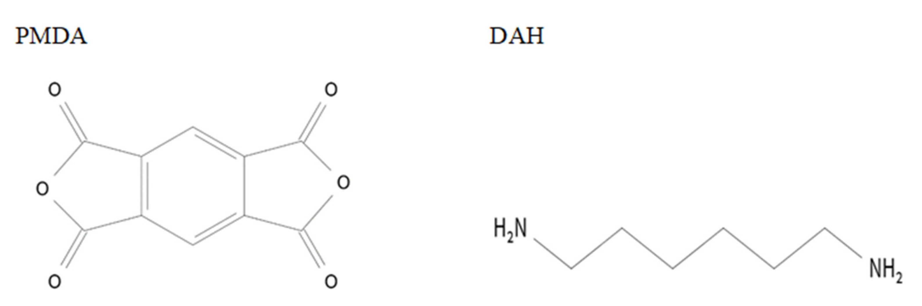
12]. Polyimide layers were deposited from 1,2,3,5-benzenetetracarboxylic anhydride (97%, pyromellitic dianhydride, PMDA, Sigma-Aldrich) and 1,6-diaminohexane (98%, DAH, Sigma-Aldrich) (
Figure 1) as described earlier [
20]. The source temperatures were 79 °C for AlCl
3, 135 °C for TiF
4, 160 °C for PMDA, and 40 °C for DAH. The substrates were either 5 cm × 5 cm Si wafer pieces or 5 cm × 5 cm ITO (indium tin oxide) covered glass.
PI films have reasonable deposition rates below 200 °C [
20] and AlF
3 thin films can be deposited in the range of 160–340 °C [
12]. At 170 °C the deposition rate of AlF
3 on Si substrate is ~2.75 Å/cycle, while the deposition rate of PI is ~5.4 Å/cycle. These both are close to their maximum deposition rates. In addition, AlF
3 films deposited at 170 °C are amorphous and thus relatively smooth, thus avoiding extensive roughening of the nanolaminate stack structures. Therefore, 170 °C was chosen as the deposition temperature for the AlF
3 and PI nanolaminates.
Two kinds of nanolaminates with different bilayer orders were prepared (
Figure 2), starting the depositions with either AlF
3 or PI. In total 5 PI/AlF
3 bilayers were deposited, where the nominal single layer thicknesses were 10 nm. The samples therefore had a structure of 5 × (10 nm PI + 10 nm AlF
3)/substrate and 5 × (10 nm AlF
3 + 10 nm PI)/substrate. The films with the AlF
3 as the bottom layer and PI as the top layer are denoted more shortly PI-AlF
3, and the films with PI as the bottom layer and AlF
3 as the top layer are denoted AlF
3-PI. The total thicknesses of these nanolaminates were approximately 100 nm. In order to compare differences in the electrical properties, thinner 60 nm nanolaminate films with three bilayers were also prepared as 3 × (10 nm PI + 10 nm AlF
3)/substrate.
Based on the earlier experiments [
12,
20], the pulsing sequence for the AlF
3 deposition was selected as: 0.5 s pulse and 1.0 s N
2 purge for AlCl
3, 1.0 s pulse and 1.5 s N
2 purge for TiF
4. At the deposition temperature of 170 °C, a deposition rate of 2.75 Å/cycle was measured for AlF
3. Uniform PI films were obtained when the PMDA pulsing time was 1.5–7.0 s and the DAH pulsing time was 1.0–5.0 s at 170 °C. Considering the uniformity and integrity of the PI films, 2.0 s pulse and 3.0 s N
2 purge for DAH, and 5.0 s pulse and 5.0 s N
2 purge for PMDA were selected resulting in a deposition rate of 5.4 Å/cycle.
A Hitachi S-4800 (Hitachi High-Technologies Corporation, Tokyo, Japan) field emission scanning electron microscope (FESEM) and an Oxford INCA 350 (Oxford Instruments, Abingdon, UK) energy dispersive X-ray spectrometer (EDX) were used to image and analyze the composition of the nanolaminate films. Approximately 2 nm Au-Pd was sputtered onto the samples using a Cressington 208HR High Resolution Sputter Coater (Cressington Scientific Instruments, Watford, UK) to obtain clearer cross-section images from the nanolaminates. X-ray reflectivity (XRR) was measured with a PANalytical X’Pert Pro MPD X-ray diffractometer (Malvern Panalytical, Malvern, UK) to analyze the true thicknesses of the single layers in the nanolaminate stacks. The measured data was fitted using Reflex v44 [
32]. The overall thickness of the nanolaminate was measured by a FS-1™ Multi-Wavelength Ellipsometer from Film-Sense (Kurt J. Lesker Company, Frankfurt, Germany).
Atomic force microscopy (AFM) images to analyze surface roughness and morphology were recorded using a Veeco Multimode V instrument (Veeco Instruments, Plainview, NY, USA). A silicon probe with a nominal tip radius of 10 nm and a nominal spring constant of 3 N/m (Bruker RFESP-75, Billerica, MA, USA) was used to capture images in the air. Images were flattened to remove artifacts caused by sample tilt and scanner bow. Roughnesses were calculated as a root-mean-square value (Rq) as an average of 3 to 5 images per sample. The final images were obtained by scanning at a frequency of 0.5 Hz from a scanning area of 500 nm × 500 nm without any other image processing.
For electrical measurements, capacitors were made with the nanolaminate as a dielectric and ITO and Al films as the electrodes. The nanolaminate films were deposited on ITO films on glass, and Al electrodes were patterned on top by evaporating aluminum through a shadow mask by an Electron Beam Evaporator IM9912 (Telemark, Battle Ground, WA, USA). A contact to the bottom ITO electrode was made in the corner of the sample by scratching through the nanolaminate and soldering a wire. The capacitance C of the nanolaminate film was measured at zero to ±2 V bias with a 4284 A Precision LCR Meter from Hewlett Packard (Hewlett Packard, Palo Alto, CA, USA). From the measured capacitance the dielectric constant ε
r (also called as k) was calculated as
where d is the thickness of the entire nanolaminate film, ε
o is the dielectric constant of vacuum, and A is the area of the top Al electrode (2.04 × 10
−7 m
2). Leakage measurements were carried out by a Keithley 2450 Source Meter (Keithley Instruments, Cleveland, OH, USA) with ±50 V as the measurement voltage range for the 5 bilayer films and ±25 V for the 3 bilayer films.
3. Results and Discussion
3.1. Film Deposition
First it was verified that AlF
3 and PI can be deposited on top of each other at 170 °C with the same growth rates as they grow on Si substrates. On this basis it was calculated that 35 cycles of the AlF
3 process and 20 cycles of the PI process would result in a nanolaminate where the individual layer thicknesses would be 10 nm. Such bilayers were repeated for five times (
Figure 2) and with an ellipsometer it was verified that the total thicknesses of the nanolaminates were close to the targeted 100 nm.
It was observed with FESEM that the films were of lower quality if no delay time was introduced between the processes. Therefore, we tested 0, 1, 3, and 5 min breaks between the AlF3 and PI film depositions, which allows for a comparison of the effect of the delay time on the properties of the nanolaminate film, as will be described in the following.
3.2. Film Structure and Morphology Analysis
Because of the low deposition temperature all the films were amorphous. In the previous study on the ALD of AlF
3 first small signs of crystallization were observed only at 280 °C [
12].
FESEM was used to examine surface morphology of the nanolaminate films.
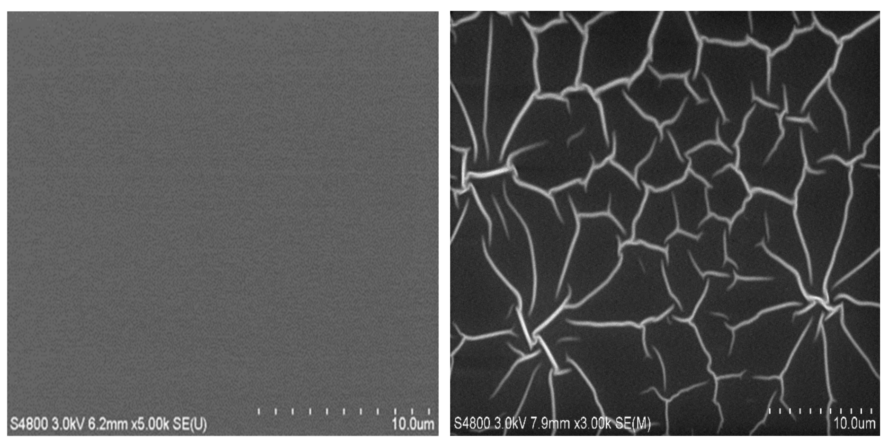
Figure 3 and
Figure 4 show the effect of the ambient atmosphere to the film surface. It can be seen that right after the deposition the nanolaminate film has a featureless surface as characteristic to amorphous films, but with a prolonged exposure to air the film surface becomes uneven as some lines appear on the surface. This was not observed in the case of 100 nm thick AlF
3 and PI films alone but in the nanolaminates it occurred regardless whether the top layer was AlF
3 or PI. The effect of the air exposure to the film morphology can be seen also from the cross-sectional images (
Figure 5). In the sample exposed for 3 min to the ambient atmosphere, all the layers, including the top PI film, are smooth, while pronounced buckling of the layers and discontinuity of the topmost layer can be seen after one day exposure. However, all the other layers except the topmost one remain continuous which is crucial for the insulating properties as seen later. It is expected that when the stacks were exposed to air, the topmost 10 nm film would be too thin to resist compressive stress.
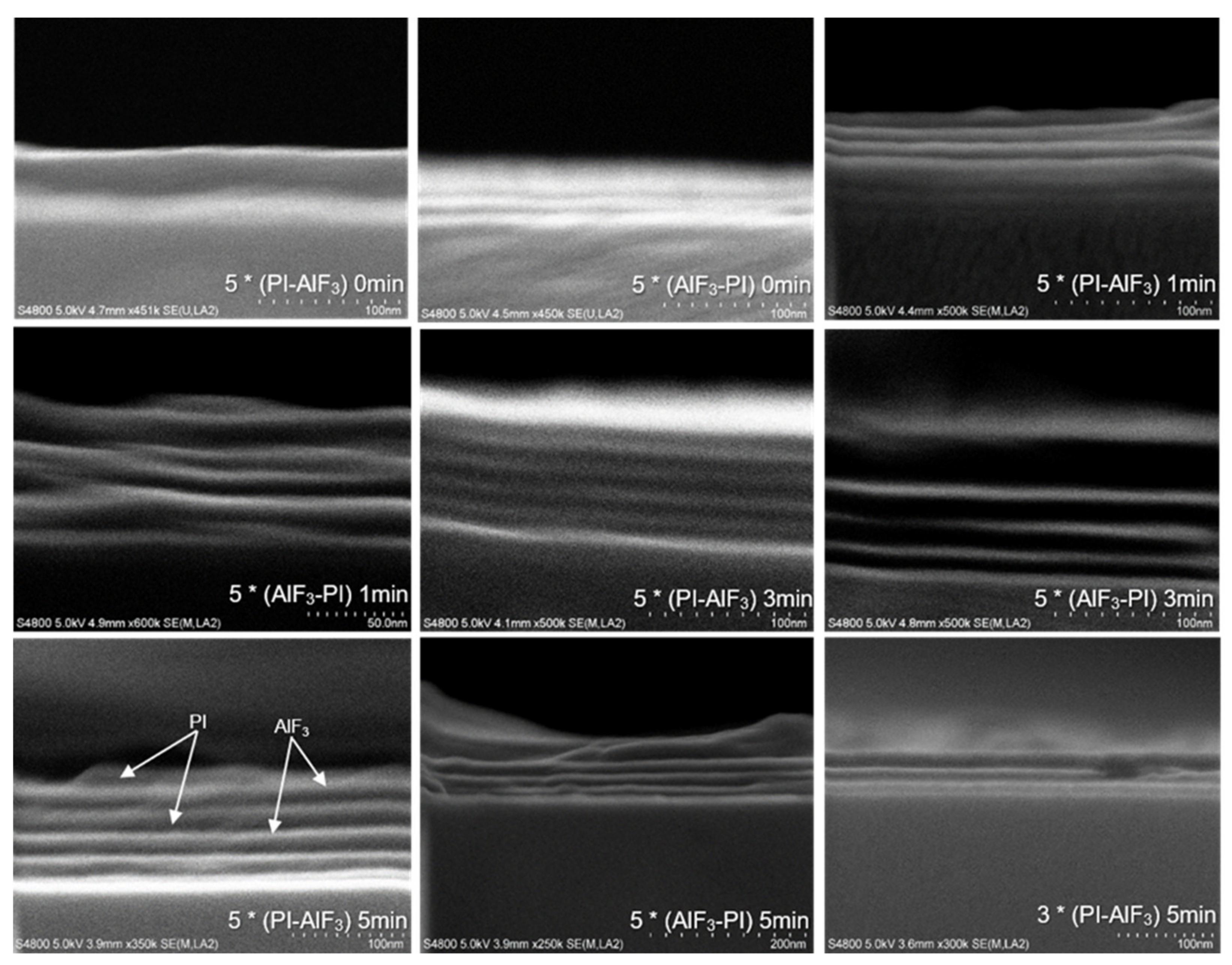
Each layer can be distinguished clearly in most of the SEM cross-section images (
Figure 6). The pictures show the effect of delay time on the nanolaminate structure. Only when there was no delay time in between the AlF
3 and PI depositions, the multilayer structure is hard to resolve. When the delay time was increased from 0 min to 5 min, the interfaces between the AlF
3 and PI layers became clearer.
EDX measurements revealed that both the PI-AlF
3 and AlF
3-PI films contained Al, F, C, O as major constituents as expected. Chlorine impurities were also detected from the nanolaminate films deposited with short delay times between the PI and AlF
3 processes. The most probable reason for the chlorine is the presence of unreacted or only partially reacted AlCl
3 precursor or byproducts originating from AlCl
3. The amount of chlorine decreased with increasing delay time, which seems to link to the improved morphology and purity of the films. However, the growth rates remained the same even if sufficient delay times were applied between the processes. As shown in
Figure 6, the number of bilayers (3 or 5) does not affect the cross-section structure.
AFM images (
Figure 7) reveal that the nanolaminate films are smooth when measured from 500 nm × 500 nm areas between the buckle lines. Roughnesses of all the ~100 nm thick films were in the range of 0.3–0.5 nm. The deposition sequence of AlF
3 and PI was found to affect only slightly the roughness of the films. Generally, the AlF
3-PI nanolaminates were slightly rougher than the PI-AlF
3 counterparts. The roughest films (R
q ≈ 0.5 nm) were AlF3-PI deposited without any delay between the processes, and the smoothest film (R
q ≈ 0.3 nm) was PI-AlF
3 deposited with 5 min delay. Although the deposition temperature of 170 °C is below the AlF
3 crystallization temperature of 280 °C [
12], AlF
3 appears to have grainier structure than PI.
The delay time between the processes also affected the roughness of the film surface. As the delay time was increased, the film surface became smoother. The total thickness of the film affects the roughness of the surface only slightly; the film with three bilayers is only slightly smoother than the films with five bilayers.
Despite the buckled lines, the amorphous nanolaminates had low enough roughness for XRR to resolve the nanolaminate stack structure (
Figure 8). In the patterns, the high frequency oscillation comes from the total thickness whereas the lower frequency oscillation arises from the single layers.
As expected from the FESEM images, clear differences were seen in the XRR curves. A 5 min delay time between the depositions of the layers resulted in more regular structures. Overall, when shorter delay times were applied, the XRR curves became more irregular. This indicates that the layered structure is not so well defined. Comparing the PI-AlF3 and AlF3-PI structures, it can be observed that a sharper nanolaminate structure was obtained when the deposition was initiated with AlF3 (PI-AlF3). With the optimized process parameters, the nanolaminate structure was retained regardless of the number of AlF3/PI bilayers. However, there were always some imperfections apparently due to less sharp interfaces and film buckling.
The XRR curve of the PI-AlF
3 nanolaminate deposited with 5 min delay in between the PI and AlF
3 processes was analyzed in detail (
Figure 9 and
Table 1). The total thickness of the nanolaminate film was 95.2 nm, which is only slightly less than the targeted 100 nm. It can be seen from
Table 1 that as the number of the deposited layers increases, the roughnesses of the interfaces generally increase. The scattering length density (SLD) of AlF
3 is from 2.2–2.3 × 10
−5 Å
−2 and also for PI SLD varies in only a narrow range of 1.2–1.4 × 10
−5 Å
−2. These equal to mass densities of 2.7–2.8 g/cm
3 for the AlF
3 stoichiometry and 1.4–1.5 g/cm
3 for PI when a repeating monomeric unit of C
16H
14N
2O
4 [
20] is used for the calculation.
The thicknesses of the first AlF
3 and PI layers on the Si substrate were somewhat less than expected from the growth rates measured at the steady-state growth conditions. Further layers deposited on top of each other had constant thicknesses and hence deposition rates. These thicknesses were not exactly 10 nm, however, indicating slight differences from the growth on silicon. When evaluating the nanolaminate stack structure as a function of a location of a given bilayer, it was seen that the thickness of the AlF
3 layer tends to stabilize at 9.5 nm (~0.5 nm lower than the expected 10 nm) regardless of the layer position in the stack. On the other hand, the PI layers were always slightly thicker than the preceding PI layers in the stack (0.3–1 nm) with the exception of the topmost layer that was much thinner (2.3 nm). This is due to the shrinkage when the sample is exposed to air for a long time, as also seen in FESEM images (
Figure 3 and
Figure 4).
3.3. Electric Properties
Dielectric constants and leakage properties of selected structures were measured by depositing the nanolaminates onto ITO films on glass substrates. Al evaporated through a shadow mask was used as the top electrode for the capacitor. The total thicknesses and dielectric constants of different structures are shown in
Table 2.
For a bare 75 nm AlF3 film, a dielectric constant of 3.4 was measured, and the bare PI film has a dielectric constant 3.8. Thicknesses of the measured five bilayer nanolaminate stacks were 90–100 nm. Interestingly the dielectric constants of the nanolaminate films are within 3.8–4.8, being higher than those of AlF3 film (3.4) and PI film (3.8) alone, whereas an intermediate value would be expected as the first approximation. A plausible explanation for the higher than expected dielectric constant is interface polarisation within the nanolaminate structures, which in turn may arise from the leaky nature of the PI films (see below).
Generally, the dielectric constants of the nanolaminate stacks with PI as the top layer are smaller compared to the AlF3-PI stack. As the delay times between the AlF3 and PI processes were increased, the dielectric constant showed an increasing trend, closely attributed to the improved layered structure of the nanolaminates.
Leakage currents and breakdown voltage of the nanolaminates deposited with 5 min delay were measured from the samples deposited onto ITO films and completed by the Al top electrodes. Bare AlF
3 and PI films were also measured for comparison, as shown in
Figure 10.
The bare 75 nm thick AlF3 exhibited good insulating properties: a high breakdown voltage of 96 V and low leakage current density (<10−6 A/cm2) up to the breakdown voltage which are characteristics of good inorganic insulating materials. The leakage current density of the bare PI by contrast was very high and breakdown voltage low. All the nanolaminates exhibit leakage properties that are closer to AlF3 than PI, i.e., low leakage current densities and high breakdown voltages. For such thin films deposited at low temperature and containing organic constituent, leakage current densities less than 10−5 A/cm2 and breakdown voltages of more than 50 V are excellent results. As can be expected, the thinner nanolaminate film (PI-AlF3 5 min, with three bilayers) has a lower breakdown voltage and a higher leakage current density than the thicker nanolaminates. Replotting the results as a function of electric field instead of absolute voltage would bring it together with the other nanolaminates, however.
The leakage current density through the bare AlF
3 film was more stable than through the nanolaminate films, which is the most obvious within the 0–10 V range (
Figure 11). In this regard, we conducted several sets of comparison experiments where the leakage measurement was repeated several times. The five and three bilayer nanolaminates were measured repeatedly within ±40 V and ±25 V, respectively. Upon repetition the leakage level increased and the noise decreased. This refers to a growth and stabilization of leakage paths that in the first measurements cause the noisy behavior. Because of the high leakage of PI, low leakage of AlF
3, and the lack of noisy leakage in bare AlF
3, it is obvious to relate the instability to the PI layers in the nanolaminates.


 ,
, 


