Abstract
Resistive random-access memory (RRAM) devices are noticeable next generation memory devices. However, only few studies have been conducted regarding RRAM devices made of alloy. In this paper, we investigate the resistive switching behaviors of an Au/Ti/HfTiOx/p-Si memory device. The bipolar switching is characterized depending on compliance current under DC sweep mode. Good retention in the low-resistance state and high-resistance state is attained for nonvolatile memory and long-term memory in a synapse device. For practical switching operation, the pulse transient characteristics are studied for set and reset processes. Moreover, a synaptic weight change is achieved by a moderate pulse input for the potentiation and depression characteristics of the synaptic device. We reveal that the high-resistance state and low-resistance state are dominated by Schottky emissions.
1. Introduction
Over the years, traditional memory devices such as dynamic random-access memory (DRAM) and NAND flash devices have had an enormous impact on the development of Information Technology (IT). However, downscaling the size of DRAM has faced physical limitations and NAND flash has a slow operation speed, so there is a growing need for new memory devices with high performances [1]. To overcome these kinds of challenges, resistance-based memory devices have been invented. These include magnetic random-access memory (MRAM) [2], phase-change random-access memory (PRAM) [3], and resistive random-access memory (RRAM) devices. Among these new types of memory, RRAM is in the spotlight thanks to numerous advantages such as fast switching, low power consumption, complementary metal-oxide semiconductor (CMOS) compatibility, and high-density integration with three dimensional (3D) vertical structures [4,5,6]. A RRAM stack is usually of a metal–insulator–metal (MIM) or metal–insulator–semiconductor (MIS) structure akin to a capacitor [7]. It can be divided into two states: a high-resistance state (HRS) and low-resistance state (LRS), which can indicate 0 and 1 as the state of the memory device [8,9,10]. The initial state of RRAM is a HRS. When voltage is applied to the RRAM, a soft breakdown occurs in the insulator and this lowers the resistance of RRAM, hence this leads to a the LRS. There are two typical switching behaviors: one is unipolar switching and the other is bipolar switching [11]. Under unipolar switching, the set and reset processes occur at the same voltage polarity and the amplitude of voltage is the main factor for the resistive switching. Usually, the set process occurs at a higher voltage amplitude than the reset process. Under bipolar switching, the set and reset processes occur at the opposite voltage polarity and here the polarity is the main factor for resistive switching. The common resistive switching behavior of RRAM nowadays due to its superior resistive switching performances, such as endurance and low-current operation. There are several common uses for RRAM. Storage-class memory (SCM) can reduce the latency gap between CPU and DRAM [12]. RRAM can mimic the synapses of the human brain for neuromorphic computing [13,14,15]. The appropriate RRAM for each application is determined by the switching characteristics and the switching mechanism can determine the resistive switching. The mechanism of resistive switching of filamentary type RRAM is the formation and rupturing of conduction filament (CF). The CF type RRAM can be divided into three categories [16,17,18]. The first is an electrochemical metallization mechanism (ECM). In this type of RRAM, the conduction filament is made of metal active electrodes, such as Ag or Cu. The metal filament is formed when the top electrode (TE) is subjected to positive voltage and it is ruptured vice versa [19]. The second is the valence change mechanism (VCM) [19]. In this case, the oxygen vacancy serves for the formation and rupturing of the filament. Under a positive voltage, oxygen ions drop from their original position and causes oxygen vacancy. The last one is a thermochemical mechanism (TCM) [20]. The main reason of resistive switching is Joule heating. The formation of CF is caused by pyrolysis of memory medium. The reset process can be achieved by melting of CF by heating. The best way to determine if RRAM is CF type is to check the DC I-V curve. These kinds of RRAM I-V curves show at least one abrupt resistive switching between set and reset [21]. The resistance switching in the interface type is overall, while that of CF type is localized. This means it has better uniformity than CF type RRAM. The main reason for the resistive switching of interface type RRAM is the modulation of oxygen ions. This happens at the interface between the metal electrode and the oxide due to the modulation of the Schottky barrier [22]. The narrowing of the tunneling barrier enables resistive switching. To verify the resistive switching mechanism of the interface type conducting path, a bunch of switching models have been issued, such as electrochemical migration of oxygen vacancies, trapping of charge carriers (hole or electron), and a Mott transition induced by carriers doped at the interface [23]. These kinds of RRAM I-V curves show gradual resistive switching for both set and reset processes [21]. Although a filamentary RRAM can also ensure multilevel conductance by switching compliance current, it is even easier to achieve this with interface type RRAM, thanks to this gradual resistive switching feature [24]. This means it can be used for biological synapsis for neuromorphic computing. Neuromorphic computing is the new computing system for substituting traditional von Neumann computing. Von Neumann computing has an enormous impact on the development of IT but it has the bottleneck problem owing to physical separation [25]. However, neuromorphic computing can undertake storing and computation at the same time so it is a likely substitution of von Neumann computing. When using an RRAM device as an artificial synapse, the MLC capability of RRAM is important. In other words, having multiple states of the applied pulse improves the performance of the neuromorphic system when performing a task such as pattern recognition [21].
In this paper, the resistive switching behaviors of a Ti/HfTiOx/p++-Si RRAM device are investigated. The synaptic properties of an alloyed type high-k material such as HfTiOx have seldom been reported in the past. Theoretical works of HfTOx and HfAlOx-based RRAM systems were studied, which reveals that resistive switching can be altered by the dopant concentration and dopant material [26,27]. Additionally, the measurement results including the variability and retention were reported in HfAlOx-based RRAM devices [28,29,30]. The silicon bottom electrode has some advantages over the metal electrode. First, the resistive switching behavior can be changed by the doping concentration of silicon surface [31]. Second, for embedded memory, the silicon bottom electrode can be directly connected to the source or drain of the MOSFET [32].
2. Experiments
RRAM devices were fabricated on the commercially available highly doped (>1019 cm−3) p-Si/SiO2 (~300 nm) substrate. Initially two different areas of 10 × 10 µm2 and 25 × 25 µm2 SiO2 (hole structures) were etched via a conventional photolithography process for adjacent top (TE) and bottom contact (BE), respectively, for the RRAM devices. SiO2 was completely etched by 160 s wet etching in buffer oxide etchant (BOE) for the hole structures. A switching layer was deposited by the atomic layer deposition technique with 7 supercycles of 10 laminated alternate cycles of HfO2 (7.4 Å with a growth rate of 0.74 Å/cycle) and TiO2 (2.3 Å with a growth rate of 0.23 Å/cycle), respectively. Tetrakis (ethylmethylamino), hafnium (TEMAHf) and titanium tetraisopropoxide (TTIP) were used as Hf and Ti precursors with H2O as the oxidant at a deposition temperature of 280 °C. For bottom electrode contact, laminated HfTiO layers were etched by BOE. Finally, top and bottom electrodes were fabricated via photolithography and e-beam deposition of Ti (5 nm)/Au (50 nm) with lift-off process in acetone with areas of 50 × 50 µm2 and 100 × 100 µm2, respectively.
Fabrication flow is depicted in 5 steps in Figure 1a–e. All the resistive switching properties were obtained by a Keithley 4200 SCS semiconductor parameter analyzer along with pulse generator with sweeping voltage on the TE keeping BE to the ground.
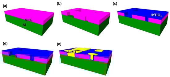
Figure 1.
Fabrication process of Au/Ti/HfTiOx/p-Si device in contact hole structure: (a) SiO2 deposition as mold layer; (b) etching process after patterning; (c) HfTiOx layer deposition; (d) etching process of bottom electrode; (e) Au/Ti deposition into contact hole.
3. Results and Discussion
The 5 nm thick Ti layer in the Au/Ti/HfTiOx/p-Si device can act as a scavenger of oxygen. Ti is easily oxidized, bringing oxygen to the layer of HfTiOx and leading to oxygen vacancies at the HfTiOx layer. Figure 2a,b show the I-V curve of the Au/Ti/HfTiOx/p-Si device. The set and reset processes are observed in DC sweep mode under different compliance current (CC) conditions of 100 μA and 1 mA. The set process was performed at a positive voltage while the reset process was performed at a negative voltage. The LRS variation occurred due to the current overshoot during the set process. The conducting filament growth was not perfectly controlled even though the same CC was applied to the device. On the other hand, the HRS variation was of a stochastic nature when the filament ruptured. The current dropped abruptly under switching and the final HRS was reached in several steps under other switching. The resistive switching failure is depicted in Figure 2c. The full reset of the device happened when the current overshoot occurred with a negative bias. The conducting filament can be fully ruptured when strong Joule heating occurs [33]. It is difficult to conduct the set process again after the full reset occurs.
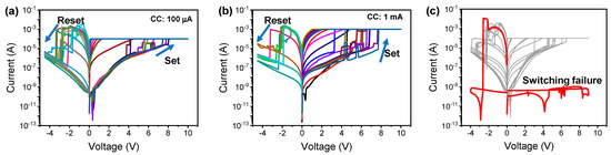
Figure 2.
I-V characteristics of Au/Ti/HfTiOx/p-Si device with compliance current (CC) of (a) 100 μA and (b) 1 mA. (c) Resistive switching failure by full reset process.
Figure 3a,b show the set voltage (VSET) and reset voltage (VRESET) distributions of Au/Ti/HfTiOx/p-Si device as a function of CC. VSET and VRESET are not particularly affected by CC. However, the reset current (IRESET) is slightly increased with increasing CC, indicating that in general a larger conducting filament is formed at a larger CC.
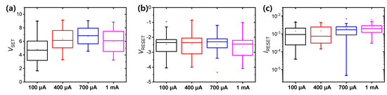
Figure 3.
(a) Set voltage, (b) reset voltage, and (c) reset current distributions of Au/Ti/HfTiOx/p-Si device.
Figure 4 shows the retention property of the Au/Ti/HfTiOx/p-Si device in the LRS and HRS. The LRS and HRS were extracted at a read voltage of 0.5 V. Two states did not change significantly for 10,000 s, indicating this device has nonvolatile memory.
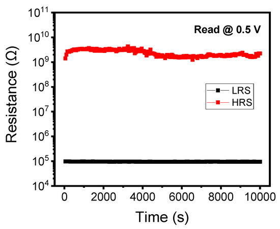
Figure 4.
Retention test of Au/Ti/HfTiOx/p-Si device in the low-resistance state (LRS) and high-resistance state (HRS) for 10,000 s.
Next, we investigated the pulse operation of the Au/Ti/HfTiOx/p-Si device. The pulse with positive voltage of 6 V and pulse width of 300 μs was applied to the device for the set operation in Figure 5a. About 100 μs after the set pulse was applied, the current started to increase rapidly and overshot up to more than 7 mA. The increased current level was detected by read pulses with 1 V before and after the set pulse. The reset pulse with −4 V and read pulse with 1 V were used for the reset process in Figure 5b.
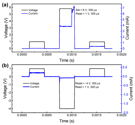
Figure 5.
Pulse transient characteristics of Au/Ti/HfTiOx/p-Si device for (a) set process and (b) reset process.
Next, the potentiation and depression were conducted in the Au/Ti/HfTiOx/p-Si device by applying repetitive pulses. For the potentiation, 36 consecutive pulses with an amplitude of 3 V were applied to the device in Figure 6a. The conductance was extracted by the read pulse with 0.5 V after each pulse for potentiation or depression in Figure 6a,b. Although the conductance decreases or maintains at a few points, in most cases, the conductance value gradually increased with repeated pulses. Similarly, for the depression, the 36 consecutive pulses with a pulse voltage of −2.2 V decreased the conductance linearly. Of the 36 pulse responses, only four cases show the opposite tendency and others were all decreased with pulses. To evaluate the linear update of the conductance in the potentiation and depression, nonlinearity (NL) is defined by the formula NL = average (|(G − Glinear)/G| × 100), where G is the conductance value and Glinear is the conductance of the ideal case. The NLs of potentiation and depression are 29.25% and 7.29%, respectively, in Figure 6c.
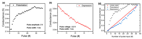
Figure 6.
(a) Potentiation, (b) depression, and (c) normalized conductance characteristics of the Au/Ti/HfTiOx/p-Si device.
Finally, we discuss the conductance mechanism of the Au/Ti/HfTiOx/p-Si device. The I-V curves in the LRS and HRS follow the fitting for Schottky emissions rather than Ohmic conduction as the slope changed with the voltage. Figure 7a shows ln(I) versus V1/2 for Schottky emissions in which LRS and HRS are linear for this fitting except for the low-voltage region (low-electric-field region). The fitting result indicates that the electric field enhanced thermionic emission of the electron can be a main conduction of Au/Ti/HfTiOx/p-Si device. The thermionic emission equation is defined as
where J is the current density, A is the effective Richardson constant, T is the absolute temperature, q is elementary charge, ΦB is the Schottky barrier height, E is the electric field at the interface, kB is Boltzmann’s constant, εr is the dynamic dielectric constant, and ε0 is the permittivity of free space [34]. The possible conducting filament model of the Au/Ti/HfTiOx/p-Si device is depicted in Figure 7b,c. There could be an insulated gap region between the top electrode and the filament in both HRS and LRS. In the LRS by the SET process, the conducting filament will grow more, so the conductivity and Schottky barrier can be modulated.
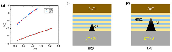
Figure 7.
(a) ln(I) versus V1/2 fitting curve of Au/Ti/HfTiOx/p-Si device in the LRS and HRS. (b) Filament evolution and gap region between Au/Ti and filament in (b) HRS and (c) LRS.
4. Conclusions
In this work, we characterize the resistive switching of an alloyed type HfTiOx-based memory device with different compliance currents. The failure mechanism for the full reset process is revealed. The device shows robust retention which is suitable for nonvolatile memory and long-term memory in synaptic devices. The set and reset transient characteristics are conducted the set pulse, reset pulse, and read pulse. The multilevel characteristics are demonstrated by multiple identical pulses, which is emulated for synaptic potentiation and depression in a neuromorphic system. Finally, the conduction mechanism is presented by the fitting process and conducting filament model.
Author Contributions
Formal analysis, B.K., C.M., H.R., M.I. and S.K.; funding acquisition, B.-D.Y.; investigation, S.K.; resources, B.-D.Y.; supervision, B.-D.Y. and S.K.; writing—review and editing, B.K., B.-D.Y. and S.K. All authors have read and agreed to the published version of the manuscript.
Funding
This work was supported in part by the National Research Foundation of Korea (NRF), grant funded by the Korean government (MSIP) under Grant 2021R1C1C1004422 and by Korea Institute of Energy Technology Evaluation and Planning (KETEP) and the Ministry of Trade, Industry & Energy (MOTIE) of the Republic of Korea (No.20194030202320).
Institutional Review Board Statement
Not applicable.
Informed Consent Statement
Not applicable.
Data Availability Statement
Not applicable.
Conflicts of Interest
The authors declare no conflict of interest.
References
- Frank, D.; Dennard, R.; Nowak, E.; Solomon, P.; Taur, Y.; Wong, H. Device scaling limits of Si MOSFETs and their application dependencies. Proc. IEEE 2001, 89, 259–288. [Google Scholar] [CrossRef]
- Maffitt, T.; DeBrosse, J.; Gabric, J.; Gow, E.; Lamorey, M.; Parenteau, J.; Willmott, D.; Wood, M.; Gallagher, W. Design consideration for MRAM. IBM J. Res. Dev. 2006, 50, 25. [Google Scholar] [CrossRef]
- Liu, T.; Zhao, Y.; Xue, C.; Li, M. Power-aware varialbe partitioning for DSPs with hybrid PRAM and DRAM main memory. IEEE Trans. Signal Proc. 2013, 61, 3509. [Google Scholar] [CrossRef]
- Li, T.; Long, S.; Liu, Q.; Lu, H.; Liu, S.; Liu, M. An overview of resistive random access memory devices. Chin. Sci. Bull. 2011, 56, 3072. [Google Scholar] [CrossRef]
- Kim, S.; Kim, H.; Hwang, S.; Kim, M.; Chang, Y.; Park, B. Analog synaptic behavior of a silicon nitride memristor. ACS Appl. Mater. Interfaces 2017, 9, 46. [Google Scholar] [CrossRef] [PubMed]
- Kim, S.; Chang, Y.; Park, B. Understanding rectifying and nonlinear bipolar resistive switching characteristics in Ni/SiNx/p-Si memory devices. RSC Adv. 2017, 7, 17882. [Google Scholar] [CrossRef]
- Maestro, M.; Martin-Martinez, J.; Diaz, J.; Crespo-Yepes, A.; Gonzalez, M.; Rodriguez, R.; Campabadal, F.; Nafria, M.; Aymerich, X. Analysis of set and reset mechanisms in Ni/HfO2-based RRAM with fast ramped voltages. Microelectron. Eng. 2015, 147, 176. [Google Scholar] [CrossRef][Green Version]
- Akihito, S. Resistive switching in transition metal oxides. Mater. Today 2008, 11, 28. [Google Scholar]
- Wong, H.; Lee, H.; Yu, S.; Chen, Y.; Wu, Y.; Chen, P.; Lee, B.; Chen, F.; Tsai, M. Metal-oxide RRAM. Proc. IEEE. 2012, 100, 1951–1970. [Google Scholar] [CrossRef]
- Chang, T.; Chang, K.; Tsai, T.; Chu, T.; Sze, S.M. Resistance random access memory. Mater. Today 2016, 19, 254–264. [Google Scholar] [CrossRef]
- Zhu, L.; Zhou, J.; Guo, Z.; Sun, Z. An overview of materials issues in resistive random access memory. J. Mater. 2015, 1, 285. [Google Scholar] [CrossRef]
- Liu, J.; Hsu, C.; Wang, I.; Hou, T. Categorization of multilevel-cell storage-class memory: An RRAM example. IEEE Trans. Electron Devices 2015, 62, 2510. [Google Scholar]
- Wu, W.; Wu, H.; Gao, B.; Deng, N.; Yu, S.; Qian, H. Improving analog switching in HfOx-based resistive memory with a thermal enhanced layer. IEEE Electron Dev. Lett. 2017, 38, 1019. [Google Scholar] [CrossRef]
- Wang, R.; Shi, T.; Zhang, X.; Wang, W.; Wei, J.; Lu, J.; Zhao, X.; Wu, Z.; Cao, R.; Long, S.; et al. Bipolar analog memristors as artificial synapses for neuromorphic computing. Materials 2018, 11, 2102. [Google Scholar] [CrossRef] [PubMed]
- Moon, K.; Lim, S.; Park, J.; Sung, C.; Oh, S.; Woo, J.; Lee, J.; Hwang, H. RRAM-based synapse device for neuromorphic systems. Faraday Discuss. 2019, 213, 421. [Google Scholar] [CrossRef] [PubMed]
- Shen, Z.; Zhao, C.; Qi, Y.; Xu, W.; Liu, Y.; Mitrovic, I.; Yang, L.; Zhao, C. Advances of RRAM devices: Resistive switching mechanisms, materials and bionic synaptic application. Nanomaterials 2020, 10, 1437. [Google Scholar] [CrossRef] [PubMed]
- Zahoor, F.; Zulkifli, T.; Khanday, F. Resistive random access memory (RRAM): An overview of materials, switching mechanism, performance, multilevel cell (MLC) storage, modeling, and applications. Nanoscale Res. Lett. 2020, 15, 90. [Google Scholar] [CrossRef] [PubMed]
- Wang, H.; Yan, X. Overview of resistive random access memory (RRAM): Materials, filament mechanisms, performance optimization, and prospects. Phys. Status Solidi RRL 2019, 13, 1900073. [Google Scholar] [CrossRef]
- Wu, M.; Ting, Y.; Chen, J.; Wu, W. Low power consumption nanofilamentary ECM and VCM cells in a single sidewall of high-density VRRAM arrays. Adv. Sci. 2019, 6, 1902363. [Google Scholar] [CrossRef]
- Choi, H.; Paik, S.; Kim, Y.; Kim, M.; Kang, Y.; Lee, S.; Jho, J.; Park, J. Facilitation of the thermochemical mechanism in NiO-based resistive switching memories via tip-enhanced electric fields. J. Ind. Eng. Chem. 2021, 94, 233. [Google Scholar] [CrossRef]
- Kim, S.; Chen, J.; Chen, Y.; Kim, M.; Kim, H.; Kwon, M.; Hwang, S.; Ismail, M.; Li, Y.; Miao, X.; et al. Neuronal dynamics in HfOx/AlOy-based homeothermic synaptic memristors with low-power and homogeneous resistive switching. Nanoscale 2019, 11, 237. [Google Scholar]
- Park, J.; Biju, K.; Jung, S.; Lee, W.; Lee, J.; Kim, S.; Park, S.; Shin, J.; Hwang, H. Multibit operation of TiOx-based ReRAM by Schottky barrier height engineering. IEEE Electron Device Lett. 2011, 32, 476. [Google Scholar] [CrossRef]
- Wang, Y.; Kang, K.; Kim, M.; Lee, H.; Waser, R.; Wouters, D.; Dittmann, R.; Yang, J.; Park, H. Mott-transition-based RRAM. Mater. Today 2019, 28, 63. [Google Scholar] [CrossRef]
- Khan, S.; Kim, S. Comparison of diverse resistive switching characteristics and demonstration of transitions among them in Al-incorporated HfO2-based resistive switching memory for neuromorphic applications. RSC Adv. 2020, 10, 31342. [Google Scholar] [CrossRef]
- Pavan, P.; Puglisi, F.; Zanotti, T. Smart logic-in-memory architecture for low-power non von Neumann computing. IEEE J. Electron Devices Soc. 2020, 8, 757. [Google Scholar]
- Zhao, L.; Clima, S.; Magyari-kope, B.; Jurczak, M.; Nishi, Y. Ab initio modeling of oxygen-vacancy formation in doped-HfOx RRAM: Effects of oxide phases, stoichiometry, and dopant concentrations. Appl. Phys. Lett. 2015, 107, 13504. [Google Scholar] [CrossRef]
- Zhou, H.; Wei, X.; Wei, W.; Ye, C.; Zhang, R.; Zhang, L.; Xia, Q.; Huang, H.; Wang, B. On the origin of enhanced resistive switching behaviors of Ti-doped HfO2 film with nitrogen annealing atmosphere. Surf. Coat. Technol. 2019, 359, 150–154. [Google Scholar] [CrossRef]
- Perez, E.; Grossi, A.; Zambelli, C.; Olivo, P.; Roelofs, R.; Wenger, C. Reduction of the cell-to-cell variability in Hf1−xAlxOy based RRAM arrays by using program algorithms. IEEE Electron Device Lett. 2017, 38, 175–178. [Google Scholar] [CrossRef]
- Traore, B.; Blaise, P.; Vianello, E.; Grampeix, H.; Jeannot, S.; Perniola, L.; De Salvo, B.; Nishi, Y. On the origin of low-resistance state retention failure in HfO2-based RRAM and impact of doping/alloying. IEEE Trans. Electron Device 2015, 62, 4029–4036. [Google Scholar] [CrossRef]
- Mahata, C.; Kim, S. Modified resistive switching performance by increasing Al concentration in HfO2 on transparent indium tin oxide electrode. Ceram. Int. 2021, 47, 1199. [Google Scholar] [CrossRef]
- Kim, S.; Cho, S.; Park, B.G. Fully Si compatible SiN resistive switching memory with large-rectification ratio. AIP Adv. 2016, 6, 015021. [Google Scholar] [CrossRef]
- Wu, Y.H.; Wu, J.R.; Hou, C.Y.; Lin, C.C.; Wu, M.L.; Chen, L.L. ZrTiOx-based resistive memory with MIS structure formed on Ge layer. IEEE Electron Device Lett. 2012, 33, 435–437. [Google Scholar] [CrossRef]
- Ielmini, D.; Nardi, F.; Cagli, C. Physical models of size-dependent nanofilament formation and rupture in NiO resistive switching memories. Nanotechnology 2011, 22, 254022. [Google Scholar] [CrossRef] [PubMed]
- Chang, Y.F.; Fowler, B.; Chen, Y.C.; Chen, Y.T.; Wang, Y.; Xue, F.; Zhou, F.; Lee, J.C. Intrinsic SiOx-based unipolar resistive switching memory. II. Thermal effects on charge transport and characterization of multilevel programing. J. Appl. Phys. 2014, 116, 043709. [Google Scholar] [CrossRef]


Publisher’s Note: MDPI stays neutral with regard to jurisdictional claims in published maps and institutional affiliations. |
© 2021 by the authors. Licensee MDPI, Basel, Switzerland. This article is an open access article distributed under the terms and conditions of the Creative Commons Attribution (CC BY) license (https://creativecommons.org/licenses/by/4.0/).