Article

Effect of Annealing Temperature on Microstructure and Resistivity of TiC Thin Films

School of Physics and Technology, Xinjiang University, Urumqi 830046, China
*
Author to whom correspondence should be addressed.
Coatings 2021, 11(4), 457; https://doi.org/10.3390/coatings11040457
Submission received: 18 March 2021 / Revised: 8 April 2021 / Accepted: 12 April 2021 / Published: 15 April 2021
(This article belongs to the Special Issue Advanced Ceramic Films and Coatings)

Abstract

:
Titanium carbide (TiC) thin films were prepared by non-reactive simultaneous double magnetron sputtering. After deposition, all samples were annealed at different temperatures under high-vacuum conditions. This paper mainly discusses the influence of deposition methods and annealing temperatures on microstructure, surface topography, bonding states and electrical resistivity of TiC films. XRD (X-ray diffraction) results show that TiC thin films can still form crystals without annealing, and the crystallinity of thin films is improved after annealing. The estimated grain size of the TiC films varies from 8.5 nm to 14.7 nm with annealing temperature. It can be seen from SEM (scanning electron microscope) images that surfaces of the films are composed of irregular particles, and when the temperature reaches to 800 °C, the shape of the particles becomes spherical. Growth rate of film is about 30.8 nm/min. Oxygen-related peaks were observed in XPS (X-ray photoelectron spectroscopy) spectra, which is due to the absorption of oxygen atoms on the surface of the film when exposed to air. Raman spectra confirm the formation of TiC crystals and amorphous states of carbon. Resistivity of TiC films decreases monotonically from 666.73 to 86.01 μΩ·cm with the increase in annealing temperature. In brief, the TiC thin films prepared in this study show good crystallinity, thermal stability and low resistivity, which can meet the requirements of metal gate applications.

1. Introduction

As the size of the metal oxide semiconductor field effect transistor (MOSFET) continues to decrease, two fatal problems arise. One is related with thinning of gate dielectric, and the other is related to short channels. A high dielectric constant (K > 3.9) and metal gate technology can solve the first problem. To solve the second problem, device architecture has to be changed [1]. However, the content of this article addresses only the first issue.
As aforementioned, in order to solve the first problem, metal gate materials are used as gate electrodes, and high-k dielectric materials are used as insulators. The requirement criteria for metal gates include suitable work functions (WF), easy to fabricate, thermal stability, compatibility with dielectric layer and low resistivity [2]. Metal gate materials can be divided into two groups: pMOS (positive MOSFET) metal gate (WF is about 4.8–5.3 eV) and nMOS (negative MOSFET) metal gate (WF is about 4.0–4.5 eV) [3]. The candidate materials for metal gate can be divided into three groups: universal mid-gap metal gate, dual work function metal gate and metal gate with tunable work functions [4]. Generally, pMOS metals are too expensive and difficult to etch, while nMOS metals will be too reactive [5]. Therefore, finding cheap and stable metal gate materials has become a research hotspot. Among the candidate metal gate materials, titanium carbide (TiC) may be one of the most suitable refractories for nMOS gates [6]. It has many unique advantages, such as being relatively inexpensive [7], having high thermal stability (melting point of 3067 °C) [8], low electrical resistivity (about 68 μΩ·cm) [9], high oxidation resistance (it oxidizes slowly in air at 800 °C), excellent chemical resistance (TiC is only attacked by HNO3 and halogens) [10] and tunable work function (4.45–5.24 eV) [8]. There are a large number of carbon vacancies in TiC, and the stability range of TiCx is very large (where x varies in the range of 0.47–0.97 without any structural changes) [11,12]. In this way, the thin film properties can be changed by alternation of the atomic fraction without any structural transition [11].
However, metal gate materials have problems of their own. One of the serious problems is threshold voltage variability due to the variability of gate work function. The variation of work function is due to the difference of preferred orientation, large grains and polycrystalline structure in electrodes [13]. Therefore, one of the most effective methods to reduce the variation of threshold voltage is to prepare metal gates with small grain sizes or amorphous states [14]. Therefore, in order to satisfy the above requirements for metal gates, many studies have been carried out. Ohmori et al. [15] expounded that the threshold voltage variation in TiN metal gate can be reduced by doping C into it to reduce the crystal size and transform it into an amorphous state. Grubbs et al. prepared Ta–W–Si–C amorphous metal gate thin films to reduce the threshold variation [16].
The deposition method and conditions influence the properties of thin films, such as films structure, phase, orientation, composition and film thickness [14]. TiC thin films have been deposited by numerous physical and chemical methods, such as chemical vapor deposition [16], reactive magnetron sputtering [17,18], non-reactive magnetron sputtering [7,19], magnetron co-sputtering [20], laser ablation [21], sol-gel method [22], atomic layer deposition [8] and electron beam evaporation [23]. Although many authors have studied these methods, few people have tried to prepare TiC thin films at low temperature by non-reactive simultaneous co-sputtering [7,24]. There are a lot of advantages of this method, such as being a simple process, inexpensive [25], low temperature deposition [7] and easy to produce for further industrial applications [26]. In addition, the structure and electrical properties of the thin film are related to the C/Ti ratio [27,28,29]. Therefore, in this method, the percentage of elements in the thin film can be conveniently determined by changing the sputtering power applied to each target, which can improve the thin film performance.
The main goal of this study is to prepare TiC thin films with small grain size, which leads the reduction in the threshold voltage variation. When the gate dimension is comparable to the grain size of the metal gate, the gate of the MOSFET device is only composed of several grains with different orientations (lead to different work functions). This causes the threshold voltage to vary from device to device since the threshold voltage is directly related to the gate work functions, which is called threshold voltage variations. Therefore, the variation of threshold voltage can be reduced by reducing the grain size. Because, in this case, when the grain size is much smaller than the gate size, the gate electrode can cover a large number of grains, and the average work function of grains contained in each gate is almost equal; thus, the difference of threshold voltage between gates can be reduced. However, too small a grain size will lead to the increase in metal gate resistivity, and it is very important to keep the balance between film resistivity and grain size by changing deposition methods and process parameters.
In this study, TiC thin films with low grain size (to reduce the change of threshold voltage) were prepared by magnetron sputtering. After deposition, all samples (Ti to C ratio of 0.74 and thickness of 610 nm) were annealed (for the sake of increasing crystallinity and eliminating defects) at different temperatures (400 to 800 °C for 20 min) under high-vacuum conditions. In the end, the effects of deposition condition and annealing temperatures on the film properties have been discussed systematically.

2. Experiment

2.1. Preparation

The TiC thin films were deposited on SiO2-coated Si substrate through non-reactive simultaneous dual magnetron sputtering (JGP450, Shenyang Zhongke Instrument, Shenyang, China) using carbon (C) and titanium Ti targets in pure argon atmosphere (purity of 99.99%). The RF (radio frequency) source was applied on the C target, while the DC (direct current) source was applied on the Ti target. The power applied to both targets was 300 W (the corresponding ratio of Ti to C atoms is Ti/C = 0.74). The growth time of thin films was set at 20 min (corresponding film thickness for this deposition time is about 610 nm). Each target was columnar in shape, 5 mm thick, 60 mm in diameter and 99.99% pure. Each target was tilted 45° relative to the substrate. The distance between the substrate and the target (Ti, C) was about 5 cm. The pressure in the reaction chamber before deposition was about 1.3 × 10⁻⁴ Pa and about 0.5 Pa during deposition. The argon flow rate for all samples was set at 10 sccm, and no heating or substrate bias was applied during deposition. After deposition, some samples were annealed at 400, 500, 600, 700 and 800 °C for 20 min under high-vacuum conditions (~10−3 pa).

2.2. Characterization

The crystal structure of the film was determined by grazing incident X-ray diffractometer (GIXRD, D8 ADVANCE, Bruker, Karlsruhe, Germany) with an incidence angle of 2°. The scanning was conducted from 20° to 90°, and the sweep rate was 5°/min. The Scherrer formula [30] was used to estimate the grain size of the film,
D = 0.9   λ β cos θ
where D is grain size, β is the full-width at half maximum (FWHM) of the Bragg peak, λ is the X-ray wave length and θ is the Bragg reflection angle.
A scanning electron microscope equipped with energy dispersion spectra (SEM/EDS, SU8010, Hitachi, Japan) was used to characterize the surface morphology, thickness and atomic percentage of the film. Atomic force microscopy (AFM, Bruker Dimension ICON, Bruker, Chicago, WI, USA) was used to measure the surface morphology and surface roughness. X-ray photoelectron spectroscopy (XPS, ESCALAB 250Xi, Thermo Fisher, Waltham, IL, USA) was used to characterize the chemical bonding state and atomic percentage of elements. A Raman spectrometer (Raman, LabRAM HR Evolution, HORIBA Scientific, Paris, France) was used to characterize the composition and state of the film. The sheet resistances were measured by a Four Point Probe (RTS-8, Suzhou Lattice Electronics Co., Ltd., Suzhou, China).

3. Results and Discussions

3.1. Structure Analysis

Figure 1 shows the GIXRD patterns of TiC thin films with thickness of 610 nm, before (as-deposited) and after annealing. For the as-deposited film, only two weak diffraction peaks (111) and (200) could be observed, indicating poor crystallinity of the film, which was because the atoms could not obtain enough energy to combine to form a crystalline state [31]. With the increase in annealing temperature, other diffraction peaks TiC (220), TiC (311) and TiC (222) of the TiC crystal began to appear. In addition, the peak (111) moved to the low diffraction angle, and it matched with the standard TiC crystal (JCPDS No.65-8805) when the temperature reached to 700 °C [9]. Furthermore, at intensity, all peaks became strengthened, and the width of them narrowed with the increase in annealing temperature compared with as-deposited thin film due to the fact that crystallinity of film was better [32]. Meanwhile, the strength of the TiC (200) peak became stronger with the increase in annealing, and the intensity of it exceeded that of the (111) peak while the temperature reached at 800 °C. The changes in intensity of these two peaks can be attributed to the competition between surface and strain energies at different temperatures [33]. In the end, one more extra peak appeared at 55.66°, which was related with TiO2 when the annealing temperature reached to 800 °C, but it could not be observed under other conditions, which may be due to the fact that at this high temperature titanium reacts with oxygen and forms crystals [11]. The average grain size of the TiC films estimated by Scherrer formula ranged from 8.5 nm to 14.7 nm. In conclusion, the annealing temperature improved the crystallinity of TiC thin films, but it did not lead to phase transition, which indicates that TiC thin films have good thermal stability.

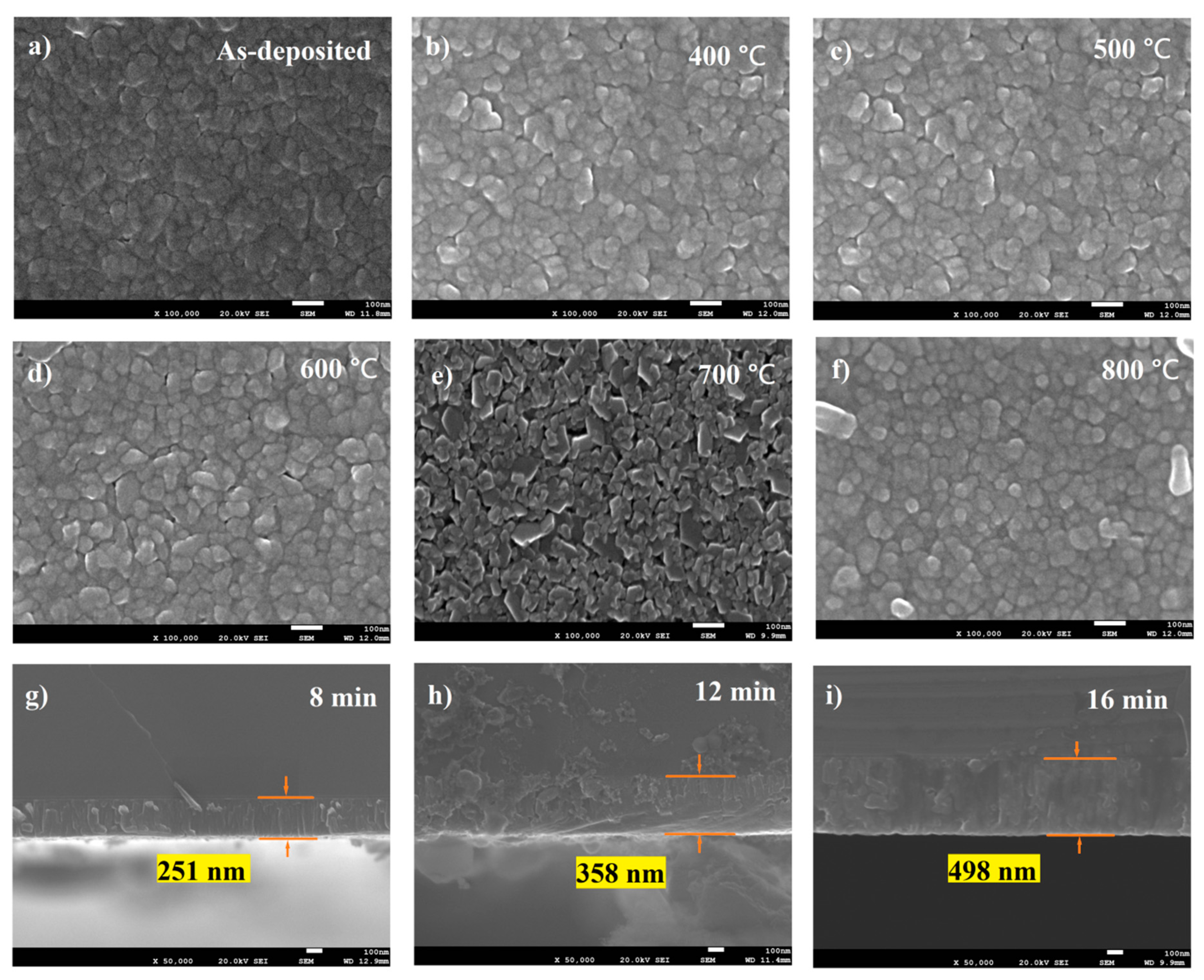
3.2. Morphology Analysis

The surface and cross-sectional morphology of TiC thin films were characterized by a scanning electron microscope (SEM). Figure 2a–f shows the surface SEM images of the as-deposited and annealed TiC films with a thickness of 610 nm. As can be seen from the scanning electron microscopy images, the surface of TiC film was composed of particles of different shapes. Then, with the increase in annealing temperature, the shape of the particles became uniform and the density increased. When the temperature reached 800 °C, the shape of the particles became spherical [17]. Estimated particle size of thin films by SEM images (40~55 nm) was much larger than XRD (8.5~14.7 nm). This difference is due to the physical error in determining the grain edges in SEM micrograph [19]. Figure 2g–i shows the SEM cross-sectional images of TiC films with different sputtering time, annealed at 800 °C. From the images it can be seen that thickness of TiC films increased linearly with the accumulations of sputtering time, and based on this, the estimated growth rate of film was about 30.8 nm/min. Continuous columnar crystals [34,35] can be observed for thin films with a thickness of 251 nm, but it was less obvious with the increase in thin film thickness.

3.3. Chemical Compositions and States

Figure 3 shows the XPS full spectrum (survey), Ti 2p, C 1s and O1s spectra of as-deposited and annealed TiC films with thickness of 610 nm. From the full spectrum (Figure 3a) Ti, C and O peaks can be identified [10]. The presence of oxygen may be due to oxidation of the film surface when exposed to air [36,37]. In order to verify this conclusion, XPS and EDS were both used in this paper to measure the atomic percentage of element in TiC, and the results are listed in Table 1.
As can be seen from Table 1, the percentage of oxygen atoms measured by XPS was larger than that measured by EDS, and the content of oxygen (in XPS) changed very little with the temperature. Mani et al. [19] observed similar behavior during heat treatment of TiC film. In their experiment, it was observed that the Ti-O-related peaks disappeared during the surface cleaning process, which could verify that the surface of the film was contaminated by oxygen molecules. In this paper, the atomic percentage of elements was determined by XPS. Furthermore, from Table 1 it can be seen that with increase in annealing temperature, content of carbon increased while content of titanium decreased due to the fact that high annealing temperature leads the dissociation of C from TiC [38], and more carbon atoms begin to diffuse from TiC beneath the surface through grain boundaries [39,40].
Figure 3b shows the Ti 2p spectra of TiC thin films for as-deposited and annealed ones. For the as-deposited film, two doublet peaks Ti 2p1/2 and Ti 2p3/2 can be observed. The Ti 2p3/2 peak exhibited two components of binding energies at 454.12 and 458.71 eV which correspond to the metallic Ti-Ti binding [17] and TiO2 phase [19], while the Ti 2p1/2 peak included two components of binding energies centered at 460.79 and 464.36 eV, which are related to TiC [34] and TiO2 [41,42] phases, respectively. With the increase in annealing temperature, the Ti-Ti correlation peak shifted to the high binding energy side, reaching 454.78 eV (close to TiC), which may be due to the further increase in oxidation degree [34], while the intensity of the TiC correlation peak decreased [43], which may be due to the increase in carbon content (dissociation from TiC).
Figure 3c shows the Ti 2p spectra of TiC thin films for as-deposited and annealed ones. For the as-deposited thin films, four main peaks were observed at 281.76, 284.82 288.47 and 286.3 eV, which are related to Ti-C, C-C [19,43], C=O [44] and C-O [42] bonds, respectively. With the increases in annealing temperature, the position of TiC-related peak shifted to the higher binding energy, and the intensity of that peak decreased, while the position of C-C peak shifted to the lower binding energy, and the intensity of that peak increased. The annealing temperature dissociates C from TiC, resulting in an increase in the content of C-C components, which leads to an increase in the intensity of the C-C correlation peak [43]. In addition, the intensity of the peak related to C=O decreases with the increase of annealing temperature, and finally disappears.
Figure 3d shows the O 1s spectra of the TiC films for as-deposited and annealed ones. For the as-deposited sample, there were only two peaks: one is probably related to TiO2 (530.12 eV) and other weak peak is related with C=O (531.62 eV) [44]. With the increase in annealing temperature, the C=O related peak disappeared while TiO2 related peak moved slightly towards the higher binding energy state.

3.4. Surface Topography Analysis

The surface morphology and roughness of TiC thin films annealed at different temperatures with a thickness of 610 nm were measured by an atomic force microscope. From the Figure 4 it can be seen that the films surface (except for annealing at 800 °C) exhibited typical hills and valley growth, where the peaks were embraced by a network of hillocks [45]. For as-deposited film, Figure 4a, there were some secondary minor hills on the big hills, which disappeared with the increase in annealing temperature. Except for the samples annealed at 800 °C, the crystal size estimated from AFM images varied from 44 to 82 nm, which was slightly larger than that estimated by XRD (8.5–14.7 nm) [46]. Furthermore, the big hills were denser with increase in annealing temperature, which is beneficial to the improvement of electric conductivity. This trend may be due to higher temperatures stimulating grain boundary migration during annealing, resulting in more grain consolidation [46]. The surface roughness of the film changed randomly (Ra = 1.49~3.23 nm, Rq = 1.90~4.59 nm.) with the increase of annealing temperature. In general, the increase in surface roughness has a negative effect on conductivity [47]. The roughness became larger at 800 °C, which may be due to the formation of metal oxide crystal [48]. According to the above discussion, we find that annealing temperature has a great influence on the structure of TiC thin films [49]. Appropriate annealing temperature (about 700 °C) can decrease the surface roughness of TiC thin films.

3.5. Raman Spectra Analysis

The amorphous carbon phase in TiC films was analyzed by Raman spectroscopy [50]. It is well known that stoichiometric TiC is non-Raman-active [51,52,53] due to the high inversion symmetry and screening effect [51]. However, non-stoichiometric TiC has been reported to be Raman-active [54].
Raman spectra obtained for as-deposited and annealed films with a thickness of 610 nm are shows in Figure 5. For the as-deposited film two strong graphite peaks can be observed approximately at 1330 (D-band) and 1581 cm−1 (G-band), called A1g mode and E2g mode [54], respectively, indicating that there was some unreacted carbon in TiC film [55]. Usually, these two bands can be assigned to breathing vibrations of sp2 carbon rings (A1g mode) and stretching vibrations of sp3 carbon rings and chains (E2g mode), respectively [53,55,56]. In addition, three peaks approximately at 269, 413 and 604 cm−1 [53,54,57] and two other weak peaks at 344 [50,52,58] and 696 cm−1 [59,60] could be observed, which correspond to the TiC phase, confirming the formation of TiC crystals [61]. Those positions of peaks are slightly difference from the aforementioned reference, and this is due to the differences in phase composition [21]. According to Oghenevweta et al. [54], these three peaks (at 269, 413 and 604 cm−1) are assigned to T2g + A1g + Eg Raman-active modes, respectively [54]. With the annealing temperature increase from 400 to 500 °C, Raman spectra remained unchanged, which indicates the stable structure of TiC thin films [40]. However, as the temperatures were at 600 °C and 800 °C, TiC-related peaks become weakened and almost disappeared, and carbon-related peaks weakened, which indicates that these two temperatures are conducive to the improvement of TiC films crystal quality [53].

3.6. Resistivity

Figure 6 shows the electrical resistivity, grain size and roughness variations with annealing temperature of as-deposited TiC films and annealed ones at different temperatures. It could be seen from the graphic that resistivity of the films decreased monotonically from 666.73 to 86.01 μΩ·cm as the annealing temperature increased to 800 °C. This change pattern of resistivity is explained as follows:
As known, electrical resistivity (ρ) can be expressed as
ρ = 1 ne μ
where n is the carrier concentration, e is the electronic charge and μ is the carrier mobility [62]. Among these three parameters, e is constant, while other two parameters μ and n are variable. We believe that a decrease in resistivity corresponds with an increase in annealing temperature because of the higher carrier concentration and mobility [63].
According to the Matthiessen’s rule [64], films resistivity can be written as
ρ = ρb + ρi + ρg + ρs
where ρb is the bulk resistivity mainly determined by composition and phase, and ρi, ρg and ρs are the resistivities related to impurities, grain boundaries and surface scattering [65]. In this study, because of no impurity was incorporated into the TiC films, the effect of impurity related with resistivity (ρi) can be ignored. In addition, the change of atomic percentages with annealing temperature was also very small, so its influence on the total resistivity can be ignored. Hence, here we only consider the effect of grain boundary and surface scattering on the resistivity.
It is well known that the increase in grain size leads to a decrease in grain boundary scattering, while the increase in surface roughness causes the increase in surface scattering [65]. Grain size and surface roughness has a contrary effect on the resistivity of the films. For the samples from as-deposited to 600 °C, the variation trends of grain size and surface roughness are consistent, shown in Figure 6, which in this case their combined effects on the film resistivity was setoff. Therefore, the main reason to generate the decrease in resistivity in this temperature region is probably ascribed to the enhancement of film crystallinity [66]. For the temperature ranges from 600 to 700 °C, the grain size increased, surface roughness decreased and crystallinity of films was better, which leads to decrease in resistivity. In the temperature range of 700~800 °C, the grain size and crystallinity of the film increased, while the surface roughness decreased, but the resistivity of the film still decreased, which may be due to the fact that the contribution of surface roughness to the resistivity of the film is less than that of grain size and crystallinity [60].

4. Conclusions

In conclusion, the deposition method and annealing temperature have great influence on the microstructure and resistivity of TiC thin films. The TiC thin films have been crystallized before annealing, and crystallinity of films has been improved with annealing. The grain size of the film was relatively small (8.5–14.7 nm) due to no heat treatment applied during depositions, but it can be adjusted by annealing. The growth rate of the TiC film was relatively high, about 30.7 nm/min. The surface of the film was composed of nanoparticles with irregular shape, and with annealing the shape of the particles became regular and dense, which is beneficial to reduce the resistivity of films. The formation of TiC can be further confirmed by XPS and Raman spectra. However, a certain amount of oxygen can be detected by XPS, which may be oxygen molecules absorbed when the film is exposed to air. The non-reactive amorphous carbon phase can also be observed from the Raman spectrum. The surface of the film was smooth (Ra = 1.49~3.23 nm, Rq = 1.90~4.59 nm), and the roughness changed randomly with the change of annealing temperature. The resistivity of the thin film was small. With the increase in annealing temperature, the resistivity of the thin film decreased monotonously from 666.73 cm to 86.01 cm. In brief, the prepared TiC film has excellent properties such as small grain size, good crystallinity and low resistivity, which can meet the requirements of a metal gate.

Author Contributions

Preparation of thin films, methodology, data analysis and writing—original draft, L.A.; conceptualization, project supervision, writing and approval for submission of the manuscript, K.T.; interpretation of data, writing—review and editing, B.S. and M.Z.; interpretation of data—review and editing, X.S.; discussion and reviewing of the manuscript, A.M.; All authors have read and agreed to the published version of the manuscript.

Funding

This research was supported by the National Natural Science Foundation of China (Grant No. 51602274), the Natural Science Foundation of Xinjiang University (Grant No. BS160210), and was sponsored by Tianshan Innovation Team Program of Xinjiang Uygur Autonomous Region (Gran No. 2020D14038).

Institutional Review Board Statement

Not applicable.

Informed Consent Statement

Not applicable.

Data Availability Statement

Data are contained within the article.

Conflicts of Interest

The authors declare no conflict of interest.

References

  1. Zhao, C.; Xiang, J. Atomic Layer Deposition (ALD) of Metal Gates for CMOS. Appl. Sci. 2019, 9, 2388. [Google Scholar] [CrossRef] [Green Version]
  2. Radamson, H.; Simoen, E.; Luo, J. CMOS Past, Present and Future, 1st ed.; Woodhead: Sawston, UK, 2018; pp. 255–263. [Google Scholar]
  3. Dadgour, H.F.; Endo, K.; De, V.K.; Banerjee, K. Grain-Orientation Induced Work Function Variation in Nanoscale Metal-Gate Transistors—Part II: Implications for Process, Device, and Circuit Design. IEEE Trans. Electron Devices 2010, 57, 2515–2525. [Google Scholar] [CrossRef]
  4. Taur, Y. CMOS design near the limit of scaling. IBM J. Res. Dev. 2002, 46, 213–222. [Google Scholar] [CrossRef] [Green Version]
  5. Robertson, J. High dielectric constant gate oxides for metal oxide Si transistors. Rep. Prog. Phys. 2006, 69, 327–396. [Google Scholar] [CrossRef]
  6. Triyoso, D.H.; Gregory, R.B.; Schaeffer, J.K.; Werho, D.; Li, D.; Marcus, S.; Wilk, G.D. Atomic layer deposited TaCy metal gates: Impact on microstructure, electrical properties, and work function on HfO2 high-k dielectrics. J. Appl. Phys. 2007, 102, 104509. [Google Scholar] [CrossRef]
  7. Olah, N.; Fogarassy, Z.; Sulyok, A.; Veres, M.; Kaptay, G.; Balazsi, K. TiC crystallite formation and the role of interfacial energies on the composition during the deposition process of TiC/a:C thin films. Surf. Coat. Technol. 2016, 302, 410–419. [Google Scholar] [CrossRef] [Green Version]
  8. Kim, C.; Ahn, H.J.; Moon, J.M.; Lee, S.; Moon, D.; Park, J.S.; Cho, B.J.; Choi, Y.; Lee, S. Temperature control for the gate workfunction engineering of TiC film by atomic layer deposition. Solid State Electron. 2015, 114, 90–93. [Google Scholar] [CrossRef]
  9. Hong, T.E.; Choi, S.K.; Kim, S.H.; Cheon, T.; Sunichi, H. Growth of Highly Conformal TiCx Films Using Atomic Layer Deposition Technique. J. Am. Ceram. Soc. 2013, 96, 1060–1062. [Google Scholar] [CrossRef]
  10. Santerre, F.; Khakani, M.A.E.; Chaker, M.; Dodelet, J.P. Properties of TiC thin films grown by pulsed laser deposition. Appl. Surf. Sci. 1999, 148, 24–33. [Google Scholar] [CrossRef]
  11. Zou, G.; Wang, H.; Mara, N.; Luo, H.; Li, N.; Di, Z.; Bauer, E.; Wang, Y.; Mccleskey, T.; Burrell, A. Chemical solution deposition of epitaxial carbide films. J. Am. Chem. Soc. 2010, 132, 2516–2517. [Google Scholar] [CrossRef] [PubMed]
  12. De Bonis, A.; Santagata, A.; Galasso, A.; Laurita, A.; Teghil, R. Formation of Titanium Carbide (TiC) and TiC@C core-shell nanostructures by ultra-short laser ablation of titanium carbide and metallic titanium in liquid. J. Colloid Interface Sci. 2017, 489, 76–84. [Google Scholar] [CrossRef]
  13. Nishi, Y. Revolutionary Nanoelectronic Devices and Processes for Post 32nm CMOS Era. ECS Trans. 2009, 19, 3–14. [Google Scholar] [CrossRef]
  14. Grubbs, M.E.; Zhang, X.; Deal, M.; Nishi, Y.; Clemens, B.M. Development and characterization of high temperature stable Ta–W–Si–C amorphous metal gates. Appl. Phys. Lett. 2010, 97, 1266–1406. [Google Scholar] [CrossRef]
  15. Ohmori, K.; Matsuki, T.; Ishikawa, D.; Morooka, T.; Yamada, K. Impact of additional factors in threshold voltage variability of metal/high-k gate stacks and its reduction by controlling crystalline structure and grain size in the metal gates. IEEE Trans. Electron Devices 2009, 1–4. [Google Scholar] [CrossRef]
  16. Alipour, R.; Meshkani, S.; Ghoranneviss, M. Specialized investigations on physical and morphological features of TiC thin films synthesized by PECVD method. Eur. Phys. J. Appl. Phys. 2015, 71, 10302. [Google Scholar] [CrossRef]
  17. Fouad, O.A.; Rumaiz, A.K.; Shah, S.I. Reactive sputtering of titanium in Ar/CH4 gas mixture: Target poisoning and film characteristics. Thin Solid Films 2009, 517, 5689–5694. [Google Scholar] [CrossRef]
  18. Dev, V. Lithium intercalation studies in cubic titanium carbide thin films. Appl. Surf. Sci. 2018, 449, 537–541. [Google Scholar] [CrossRef]
  19. Mani, A.; Aubert, P.; Mercier, F.; Khodja, H.; Berthier, C.; Houdy, P.J.S. Effects of residual stress on the mechanical and structural properties of TiC thin films grown by RF sputtering. Surf. Coat. Technol. 2005, 194, 190–195. [Google Scholar] [CrossRef]
  20. Xiang, J.; Zhang, Y.; Li, T.; Wang, X.; Gao, J.; Yin, H.; Li, J.; Wang, W.; Ding, Y.; Xu, C.; et al. Investigation of thermal atomic layer deposited TiAlX (X = N or C) film as metal gate. Solid State Electron. 2016, 122, 64–69. [Google Scholar] [CrossRef]
  21. Olah, N.; Veres, M.; Sulyok, A.; Menyhard, M.; Gubicza, J.; Balazsi, K. Examination of nanocrystalline TiC/amorphous C deposited thin films. J. Eur. Ceram. Soc. 2014, 34, 3421–3425. [Google Scholar] [CrossRef] [Green Version]
  22. D’Alessio, L.; Pace, G.; Teghil, R. Multiscale Analysis and Morphology of TiC Films Deposited by Pulsed Laser Ablation. Adv. Mater. Res. 2013, 717, 177–183. [Google Scholar] [CrossRef]
  23. Wolfe, D.E.; Singh, J. Titanium carbide coatings deposited by reactive ion beam-assisted, electron beam–physical vapor deposition. Surf. Coat. Technol. 2000, 124, 142–153. [Google Scholar] [CrossRef]
  24. Raman, K.H.T.; Kiran, M.S.R.N.; Ramamurty, U.; Rao, G.M. Structure and mechanical properties of Ti-C films deposited using combination of pulsed DC and normal DC magnetron co-sputtering. Appl. Surf. Sci. 2012, 258, 8629–8635. [Google Scholar] [CrossRef]
  25. Balazsi, K.; Vandrovcova, M.; Bacakova, L.; Balazsi, C.S. Structural and biocompatible characterization of TiC/a:C nanocomposite thin films. Mater. Sci. Eng. C 2013, 33, 1671–1675. [Google Scholar] [CrossRef]
  26. Olah, N.; Fogarassy, Z.; Sulyok, A.; Szivos, J.; Csanadi, T.; Balazsi, K.J.C.I. Ceramic TiC/a:C protective nanocomposite coatings: Structure and composition versus mechanical properties and tribology. Ceram. Int. 2016, 42, 12215–12220. [Google Scholar] [CrossRef] [Green Version]
  27. Gulbinski, W.; Mathur, S.; Shen, H.; Suszko, T.; Gilewicz, A.; Warcholinski, B. Evaluation of phase, composition, microstructure and properties in TiC/a-C:H thin films deposited by magnetron sputtering. Appl. Surf. Sci. 2005, 239, 302–310. [Google Scholar] [CrossRef]
  28. Lewin, E.; Wilhelmsson, O.; Jansson, U. Nanocomposite nc-TiC/a-C thin films for electrical contact applications. J. Appl. Phys. 2006, 100, 054303. [Google Scholar] [CrossRef]
  29. Roger, J.; Gardiola, B.; Andrieux, J.; Viala, J.C.; Dezellus, O. Synthesis of Ti matrix composites reinforced with TiC particles: Thermodynamic equilibrium and change in microstructure. J. Mater. Sci. 2016, 52, 4129–4141. [Google Scholar] [CrossRef]
  30. Shanaghi, A.; Rouhaghdam, A.R.S.; Ahangarani, S.; Chu, P.K.; Farahani, T.S. Effects of duty cycle on microstructure and corrosion behavior of TiC coatings prepared by DC pulsed plasma CVD. Appl. Surf. Sci. 2012, 258, 3051–3057. [Google Scholar] [CrossRef]
  31. Devia, D.M.; Restrepo-Parra, E.; Arangcr, P.J. Comparative study of titanium carbide and nitride coatings grown by cathodic vacuum arc technique. Appl. Surf. Sci. 2011, 258, 1164–1174. [Google Scholar] [CrossRef]
  32. Kim, J.B.; Kim, S.H.; Han, W.S.; Lee, D.J. Atomic layer deposited nanocrystalline tungsten carbides thin films as a metal gate and diffusion barrier for Cu metallization. J. Vac. Sci. Technol. A 2016, 34, 041504. [Google Scholar] [CrossRef]
  33. Arshi, N.; Lu, J.; Joo, Y.K.; Lee, C.G.; Yoon, J.H.; Ahmed, F. Study on structural, morphological and electrical properties of sputtered titanium nitride films under different argon gas flow. Mater. Chem. Phys. 2012, 134, 839–844. [Google Scholar] [CrossRef]
  34. Kataria, S.; Dash, S.; Tyagi, A. Effect of adhesive and cohesive strength on the tribological behaviour of non-reactively sputtered TiC thin films. Surf. Interface Anal. 2009, 42, 7–12. [Google Scholar] [CrossRef]
  35. Létiche, M.; Brousse, K.; Demortière, A.; Huang, P.; Daffos, B.; Pinaud, S.; Respaud, M.; Chaudret, B.; Roussel, P.; Buchaillot, L.; et al. Sputtered Titanium Carbide Thick Film for High Areal Energy on Chip Carbon-Based Micro-Supercapacitors. Adv. Funct. Mater. 2017, 27, 1606813. [Google Scholar] [CrossRef]
  36. Ignaszak, A.; Song, C.; Zhu, W.; Zhang, J.; Bauer, A.; Baker, R.; Neburchilov, V.; Ye, S.; Campbell, S. Titanium carbide and its core-shelled derivative TiC@TiO2 as catalyst supports for proton exchange membrane fuel cells. Electrochim. Acta 2012, 69, 397–405. [Google Scholar] [CrossRef]
  37. Tang, C.Y.; Wong, C.T.; Zhang, L.N.; Choy, M.T.; Chow, T.W.; Chan, K.C.; Yue, T.M.; Chen, Q. In situ formation of Ti alloy/TiC porous composites by rapid microwave sintering of Ti6Al4V/MWCNTs powder. J. Alloys Compd. 2013, 557, 67–72. [Google Scholar] [CrossRef]
  38. Aihaiti, L.; Tuokedaerhan, K.; Beysen, S.; Min, Z.; Mijiti, A. Electrical and microstructural properties of Ta-C thin films for metal gate. Mater. Res. Express 2020, 7. [Google Scholar] [CrossRef]
  39. Gao, X.; Guo, Z.; Geng, Q.; Ma, P.; Liu, G. Structure, optical properties and thermal stability of TiC-based tandem spectrally selective solar absorber coating. Sol. Energy Mater. Sol. Cells 2016, 157, 543–549. [Google Scholar] [CrossRef]
  40. Gao, X.; Guo, Z.; Geng, Q.; Ma, P.; Liu, G. Microstructure, chromaticity and thermal stability of SS/TiC-WC/Al2O3 spectrally selective solar absorbers. Sol. Energy Mater. Sol. Cells 2017, 164, 63–69. [Google Scholar] [CrossRef]
  41. Shirotori, Y.; Sawada, K.; Ozawa, K.I.; Edamoto, K.; Otani, S. Photoelectron Spectroscopy Study of the Oxidation of TiC(100). Jpn. J. Appl. Phys. 2003, 42, 1725–1731. [Google Scholar] [CrossRef]
  42. Cao, H.; Qi, F.; Ouyang, X.; Zhao, N.; Zhou, Y.; Li, B.; Luo, W.; Liao, B.; Luo, J. Effect of Ti Transition Layer Thickness on the Structure, Mechanical and Adhesion Properties of Ti-DLC Coatings on Aluminum Alloys. Materials 2018, 11, 1742. [Google Scholar] [CrossRef] [Green Version]
  43. Rüdiger, C.; Maglia, F.; Leonardi, S.; Sachsenhauser, M.; Sharp, I.D.; Paschos, O.; Kunze, J. Surface analytical study of carbothermally reduced titania films for electrocatalysis application. Electrochim. Acta 2012, 71, 1–9. [Google Scholar] [CrossRef]
  44. Nesov, S.N.; Korusenko, P.M.; Povoroznyuk, S.N.; Bolotov, V.V.; Knyazev, E.V.; Smirnov, D.A. Effect of carbon nanotubes irradiation by argon ions on the formation of SnO2−x/MWCNTs composite. Nucl. Instrum. Methods Phys. Res. Sect. B 2017, 410, 222–229. [Google Scholar] [CrossRef]
  45. Du, S.; Zhang, K.; Wen, M.; Ren, P.; Meng, Q.; Zhang, Y.; Zheng, W. Crystallization of SiC and its effects on microstructure, hardness and toughness in TaC/SiC multilayer films. Ceram. Int. 2017, 44, 613–621. [Google Scholar] [CrossRef]
  46. Lee, Y.C.; Hu, S.Y.; Water, W.; Tiong, K.K.; Feng, Z.C.; Chen, Y.T.; Huang, J.C.; Lee, J.W.; Huang, C.C. Rapid thermal annealing effects on the structural and optical properties of ZnO films deposited on Si substrates. J. Lumin. 2009, 129, 148–152. [Google Scholar] [CrossRef]
  47. Khan, A.F.; Mehmood, M.; Rana, A.M.; Bhatti, M.T. Effect of annealing on electrical resistivity of rf-magnetron sputtered nanostructured SnO2 thin films. Appl. Surf. Sci. 2009, 255, 8562–8565. [Google Scholar] [CrossRef]
  48. Khan, A.F.; Mehmood, M.; Rana, A.M.; Muhammad, T. Effect of annealing on structural, optical and electrical properties of nanostructured Ge thin films. Appl. Surf. Sci. 2010, 256, 2031–2037. [Google Scholar] [CrossRef]
  49. Fang, Z.B.; Yan, Z.J.; Tan, Y.S.; Liu, X.Q.; Wang, Y. Influence of post-annealing treatment on the structure properties of ZnO films. Appl. Surf. Sci. 2005, 241, 303–308. [Google Scholar] [CrossRef]
  50. Kumar, N.; Natarajan, G.; Dumpala, R.; Pandian, R.; Bahuguna, A.; Srivastava, S.K.; Ravindran, T.R.; Rajagopalan, S.; Dash, S. Microstructure and phase composition dependent tribological properties of TiC/a-C nanocomposite thin films. Surf. Coat. Technol. 2014, 258, 557–565. [Google Scholar] [CrossRef]
  51. Ferraro, J.R.; Nakamoto, K.; Brown, C.W. Introductory Raman Spectroscopy, 2nd ed.; Academic Press: Amsterdam, The Netherlands, 2003; pp. 95–146. [Google Scholar]
  52. Qi, Q.; Zhang, W.Z.; Shi, L.; Zhang, W.Y.; Zhang, W.; Zhang, B. Preparation of single-crystal TiC (111) by radio frequency magnetron sputtering at low temperature. Thin Solid Films 2012, 520, 6882–6887. [Google Scholar] [CrossRef]
  53. Djafer, A.Z.A.; Saoula, N.; Madaoui, N.; Zerizer, A. Deposition and characterization of titanium carbide thin films by magnetron sputtering using Ti and TiC targets. Appl. Surf. Sci. 2014, 312, 57–62. [Google Scholar] [CrossRef]
  54. Oghenevweta, J.E.; Wexler, D.; Calka, A. Study of reaction sequences during MSR synthesis of TiC by controlled ball milling of titanium and graphite. Mater. Charact. 2018, 140, 299–311. [Google Scholar] [CrossRef]
  55. Lohse, B.H.; Calka, A.; Wexler, D. Raman spectroscopy sheds new light on TiC formation during the controlled milling of titanium and carbon. J. Alloys Compd. 2007, 434, 405–409. [Google Scholar] [CrossRef]
  56. Kawashima, Y.; Katagiri, G. Fundamentals, overtones, and combinations in the Raman spectrum of graphite. Phys. Rev. B 1995, 52, 10053–10059. [Google Scholar] [CrossRef] [PubMed]
  57. Kim, Y.K.; Kim, J.P.; Park, C.K.; Yun, S.J.; Kim, W.; Heu, S.; Park, J.S. Electron-emission properties of titanium carbide-coated carbon nanotubes grown on a nano-sized tungsten tip. Thin Solid Films 2008, 517, 1156–1160. [Google Scholar] [CrossRef]
  58. Gao, X.H.; Theiss, W.; Shen, Y.Q.; Ma, P.J.; Liu, G. Optical simulation, corrosion behavior and long term thermal stability of TiC-based spectrally selective solar absorbers. Sol. Energy Mater. Sol. Cells 2017, 167, 150–156. [Google Scholar] [CrossRef]
  59. Dreiling, I.; Stiens, D.; Chasse, T. Raman spectroscopy investigations of TiBxCyNz coatings deposited by low pressure chemical vapor deposition. Surf. Coat. Technol. 2010, 205, 1339–1344. [Google Scholar] [CrossRef]
  60. Liu, H.D.; Chen, Y.M.; Yousaf, M.I.; Luo, C.; Wan, Q.; Hu, L.W.; Fu, D.J.; Ren, F.; Li, Z.G. In situ synthesized TiC–DLC nanocomposite coatings on titanium surface in acetylene ambient. Appl. Surf. Sci. 2015, 349, 93–100. [Google Scholar]
  61. Sui, L.; Wu, T.; Liu, L.; Wang, H.; Wang, Q.; Hou, H.; Guo, Q. Sensitive Pyrimethanil Sensor Based on Electrospun TiC/C Film. Sensors 2019, 19, 1531. [Google Scholar] [CrossRef] [Green Version]
  62. Li, G.; Yang, J.; Xiao, Y.; Fu, L.; Zhang, M. Effect of TiC Nanoinclusions on Thermoelectric and Mechanical Performance of Polycrystalline In4Se2.65. J. Am. Ceram. Soc. 2015, 98, 3813–3817. [Google Scholar] [CrossRef]
  63. Ali, A.H.; Hassan, Z.; Shuhaimi, A. Enhancement of optical transmittance and electrical resistivity of post-annealed ITO thin films RF sputtered on Si. Appl. Surf. Sci. 2018, 443, 544–547. [Google Scholar] [CrossRef]
  64. Timoshevskii, V.; Ke, Y.; Guo, H.; Gall, D. The influence of surface roughness on electrical conductance of thin Cu films: An ab initio study. J. Appl. Phys. 2008, 103, 113705. [Google Scholar] [CrossRef] [Green Version]
  65. Liang, H.; Xu, J.; Zhou, D.; Sun, X.; Bai, Y. Thickness dependent microstructural and electrical properties of TiN thin films prepared by DC reactive magnetron sputtering. Ceram. Int. 2016, 42, 2642–2647. [Google Scholar] [CrossRef]
  66. Hussain, A.; Ahmed, R.; Ali, N.; Butt, F.K.; Shaari, A.; Shamsuri, W.N.W.; Khenata, R.; Prakash, D.; Verma, K. Post annealing effects on structural, optical and electrical properties of CuSbS2 thin films fabricated by combinatorial thermal evaporation technique. Superlattices Microstruct. 2016, 89, 136–144. [Google Scholar] [CrossRef]
Figure 1. GIXRD patterns of as-deposited and annealed TiC thin films with a thickness of 610 nm.
Coatings 11 00457 g001
Figure 2. (af) SEM surface images of TiC thin films of before and after annealing with a thickness of 610 nm, (gi) SEM cross-section images of TiC thin films at different sputtering times with Ti/C ratio of 0.74 and annealing at 800 °C.
Coatings 11 00457 g002
Figure 3. XPS spectra for (a) survey, (b) Ti 2p, (c) C 1s and (d) O 1s of as-deposited and annealed TiC thin films with a thickness of 610 nm.
Coatings 11 00457 g003
Figure 4. AFM images and surface roughness data (Ra- Arithmetic Mean Roughness, Rq- Root-Mean-Square Roughness) of as-deposited and annealed TiC thin films with a thickness of 610 nm.
Coatings 11 00457 g004
Figure 5. Raman spectra of as-deposited and annealed TiC thin films with a thickness of 610 nm.
Coatings 11 00457 g005
Figure 6. The variations of resistivity, grain size and surface roughness with annealing temperatures for TiC thin films with a thickness of 610 nm.
Coatings 11 00457 g006
Table 1. XPS and EDS analysis of atomic content of TiC thin films with annealing temperature.
SamplesComposition by XPS (at.%)Composition by EDS (at.%)
TiCOTiCOSi
As-deposited24.5633.1442.3022.1441.7810.5125.57
400 °C23.5826.2345.84----
500 °C22.1530.8347.02----
600 °C 22.3230.3942.96----
800 °C18.1838.9038.5921.1542.9011.8624.09
Publisher’s Note: MDPI stays neutral with regard to jurisdictional claims in published maps and institutional affiliations.

