Article

Combined Processing of Micro Cutters Using a Beam of Fast Argon Atoms in Plasma

Department of High-Efficiency Processing Technology, Moscow State University of Technology STANKIN, Vadkovskiy per. 3A, 127055 Moscow, Russia
*
Author to whom correspondence should be addressed.
Coatings 2021, 11(4), 465; https://doi.org/10.3390/coatings11040465
Submission received: 16 March 2021 / Revised: 7 April 2021 / Accepted: 13 April 2021 / Published: 16 April 2021
(This article belongs to the Special Issue Technologies of Coatings and Surface Hardening for Tool Industry)

Abstract

:
We present a new method for coating deposition on micro cutters without an increase in their cutting edges radii caused by the deposition. For this purpose, the cutting edges are sharpened before the coating deposition with a concentrated beam of fast argon atoms. The sharpening decreases the initial radius and, hence, limits its value after the coating deposition. The concentrated beam of fast argon atoms is generated using an immersed in the gas discharge plasma concave grid under a negative high voltage. Ions accelerated from the plasma by the grid pass through the grid holes and are concentrated in the focal point of the grid. As a result of the charge exchange in the space charge sheaths of the grid, they are transformed into fast atoms. A uniform sputtering by the fast atoms of the micro-cutter surface reduces the radius of its cutting edge.

1. Introduction

The useful life of cutting tools substantially increases after the deposition of thin wear-resistant films [1,2]. This is due to the film hardness of about 25–30 GPa [3] exceeding by many times the hardness of the bulk material. Magnetrons [4] and vacuum arc [5] are mainly used to produce the metal vapor needed for coating synthesis. The density of magnetron discharge plasma near the product surface and the sputtering rate are substantially enhanced when pulsed DC magnetrons [6,7,8,9,10,11,12,13] are used. Metal vapor can be also produced due to sputtering a target at the bottom of a hollow cathode [14].
To prevent the formation of metal droplets in the coatings, the vacuum arc plasma can be filtered using magnetic field. An overview of filtered vacuum arc deposition systems based on magnetic ducts is presented in [15]. The droplets can be also removed from the plasma by transformation of radial plasma streams emitted by the arc cathode spots on the side surface of a cylindrical cathode into an axial stream by means of “single bottle neck” magnetic field [16]. Filtered vacuum arc with ion-species-selective bias has been applied to the synthesis of metal-doped diamond-like carbon films [17]. A magnetic island filter comprising three external coils, which generate a uniform magnetic field, and an internal coaxial coil with a cylindrical permanent magnet in its core, placed within the magnetic island, that generate a field in the opposite direction to the external field is described in [18]. Instead of coils, an internal curvilinear spiral was used in [19], which was transparent and allowed observation of the plasma movement from the arc cathode to the substrate. Analysis of the workpiece surface in [20] revealed that its roughness and the number of cathode spots show no direct relation because the current density per cathode spot does not change according to the number of cathode spots. In a pulsed vacuum arc discharge, the microparticles can be charged, and a roughly quadratic dependence of particle charge on the particle diameter was observed [21] with a 1-μm-diameter particle having a positive charge of ≈1000 electronic charges and a 5-μm-diameter particle having a charge of ≈25,000 electronic charges. Highly adherent CrN films were magnetron sputter deposited in [22] after the filtered cathodic arc etching pretreatment.
Generally, the tools are preliminarily heated and activated. Such pretreatment allows an appreciable improvement of the coating adhesion. More improvements of the adhesion and other coating properties are available when instead of DC biasing, high-voltage pulses are used [23,24,25,26].
The thicker the coating, the longer is its useful life. Nevertheless, on roughing tools with the cutting edge radii amounting to ≈15–20 µm, the coating thickness usually does not exceed 5–7 µm. At higher values of the coating thickness, the cutting edge radii grow to inadmissible values exceeding 30 µm, which are characteristic of blunted tools [27]. The 30-µm radius of the cutting edge exceeds the uncut chip thickness of micro-milling. Therefore, the material deformation mechanisms are often dominated by the plowing effect [28], and the quality of the surface is dissatisfactory [29].
The problem of cutting tools blunting caused by the coating deposition is especially acute for micro cutters with a cutting edge radius of less than 10 µm. For instance, cylindrical end-milling micro cutters work in cutting conditions, at which the depth of cut is commensurate with the cutting edge radius. It is impossible to increase the cutting stability during micro-milling through an increase in the depth of cut because of a significant degree of the tool bending. Therefore, keeping the minimum cutting edge radius is very important [30].
The minimum radius of the cutting edge will improve the cutting conditions and increase the likelihood of the cutting into the material of the whole cutting wedge, not just its tip, which can reduce cutting forces [31] and vibration [32], improve the chip formation, use cutting patterns with a minimum depth of cut at a relatively high feed per tooth, and reduce the likelihood of the workpiece abrasion.
To date, a coating with a thickness exceeding 2–3 μm cannot be deposited on micro cutters because after grinding, the radius of the cutting edge is in the range of chip thickness: about 10 μm. The wear-resistant coatings can highly improve the cutting tools’ efficiency [33,34,35,36]. However, in the case of micro tools, their cutting edge radii will increase by 2–2.5 times, which will not allow a stable cutting process. In this case, an increase in the thickness of the cut chips is impossible, because micro cutters are small and have a lower ability to resist bending, which promises their destruction when bending.
Thus, there is a limitation on the maximum feed per tooth value, and there is a minimum feed per tooth limit by the minimum chip thickness. The latter relates to the minimum allowable cutting edge radius that must be met for a stable cutting process. Chips simply will not be formed if their thickness is less than the minimum. Therefore, the only way to increase the useful life of micro cutters without losing the cutting process stability in conditions of parametric tool failure is to reduce the cutting edge radius.
Experimental investigations regarding the formation of the cutting edge geometry during an immersed tumbling process are presented in [27]. It was found that the processing time is mainly responsible for the size of the cutting edge radius. The lapping medium defines the chipping of the edge. During the experiments, micro cutters were manufactured with a cutting edge radius of ≈4.0 μm, which is lower than the values available with traditional grinding methods. Another method for diminishing the cutting edge radius based on the ELID (electrolytic in-process dressing) technique allows manufacturing cutters with the radius of approximately 3 μm [37]. However, it cannot be applied for small-sized tools.
We propose in the present study to reduce the cutting edge radius by etching the tool surface with a beam of fast argon atoms [38,39,40,41]. The etching will allow reduction of the coated tool radius lower than the radius of the initial tool.

2. Experimental

We processed end mills by Cerin (IT) under catalog number 105.030031240 with the nominal diameter of the working part amounting to 3 mm (h10) and length of 12 mm as well as the nominal angle of inclination of the chip groove equal to 30 degrees for machining light alloys, aluminum, and titanium (Figure 1). The material of the end mills is solid carbide type HM CK10-20-MG Micrograin: monocarbide (WC-94%; Co-6%) with the carbide grain size of 0.5–0.8 μm, hardness Rockwell 91.8 HRA, and transverse rupture strength 3000 N/mm2. The work surfaces of the end mills are polished and uncoated. According to the catalog, their application areas are light alloys, plastics, reinforced plastics, and titanium alloys.
While studying the bombardment by a beam of fast argon atoms, it is necessary to compare the initial geometric parameters of the cutting tools with the parameters obtained after processing. Analysis of the changes in the controlled parameters will make it possible to conclude the effectiveness of the fast atom beam. The controlled parameters were the profiles of the front surface located at different distances from the end of the cutter, as well as the angular parameters of the cutting edge, the front, and rear corners, and the cutting edge radius.
During the study, three samples of this type of end mill were measured. To control the initial geometric parameters, the algorithms of the Walter Helicheck Plus (Walter, Germany) measuring system was used, which are based on the use of machine vision methods. The measuring was carried out with cameras of transmitted and reflected light. Measurement inaccuracy by positioning stability for measuring diametrical and linear parameters does not exceed 0.32 μm. The measurement was carried out in a non-contact manner using a CCD (Charge-Coupled Device) matrix camera of transmitted light and a CCD camera of reflected light with ×400 magnification.
A hydraulic chuck with an SK 50 tool cone was used for fixing the measured samples of cutters. The obtained results of primary measurements for the working geometry of three samples are presented in Table 1.
The main geometrical parameters of a solid carbide end micro mill and radius of cutting on the radial section are shown in Figure 2. The main geometric parameters of the cutting edge were measured in three areas: A, B, and C. In the range of each area, the cutting edge radius was controlled in sets of sections: reA1, reA2, reA3, and reAn for A area, reB1, reB2, reB3, and reBn for B, and reC1, reC2, reC3, and reCn for C.
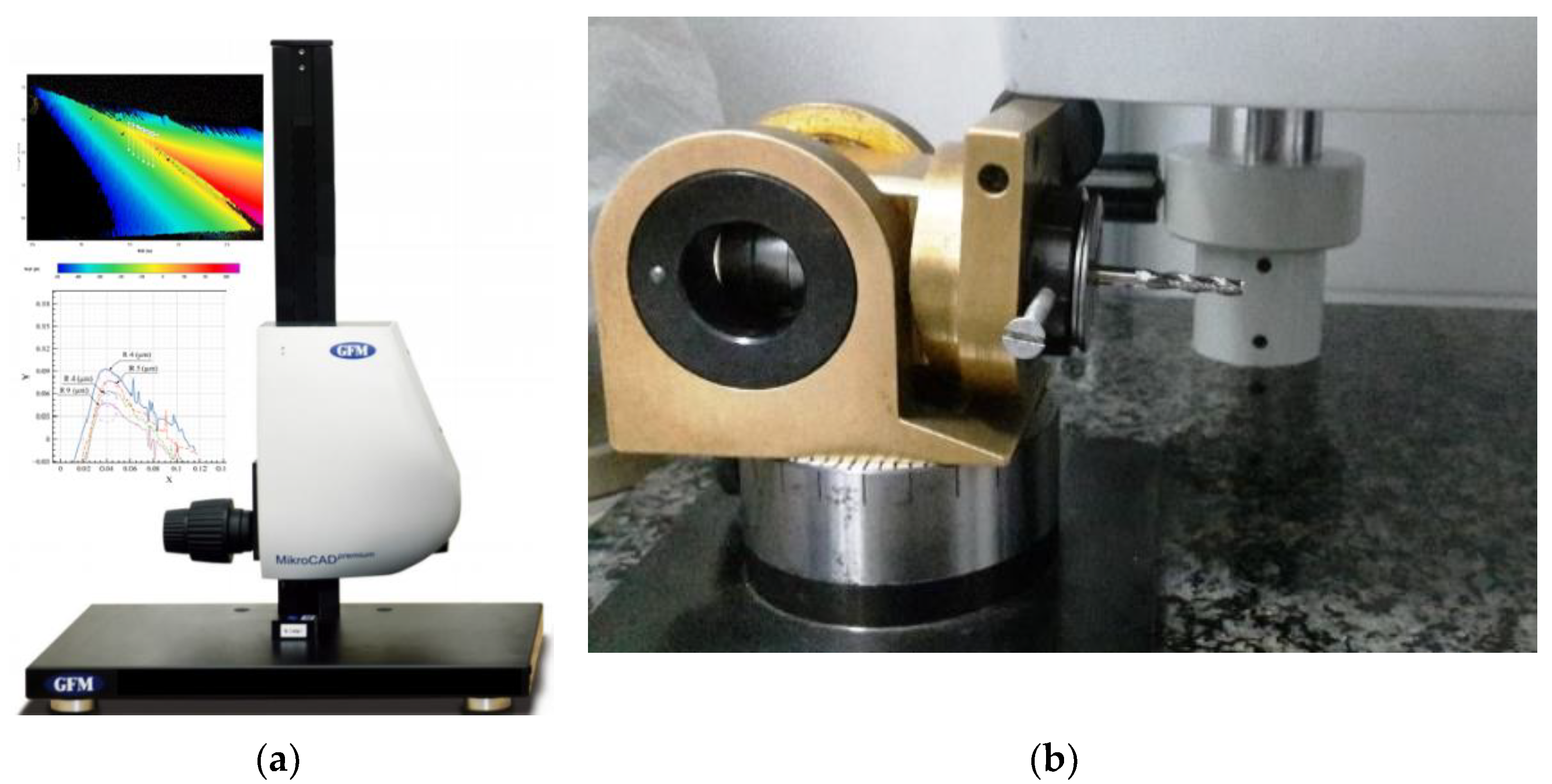
Cutting edge radius was measured with an optical 3D measuring system MicroCAD Premium plus. Its measuring algorithm is to measure a strip of light using a micromirror projector. Figure 3a shows a photograph of the measuring system and Figure 3b elucidates the measurement of the cutting edge radius.
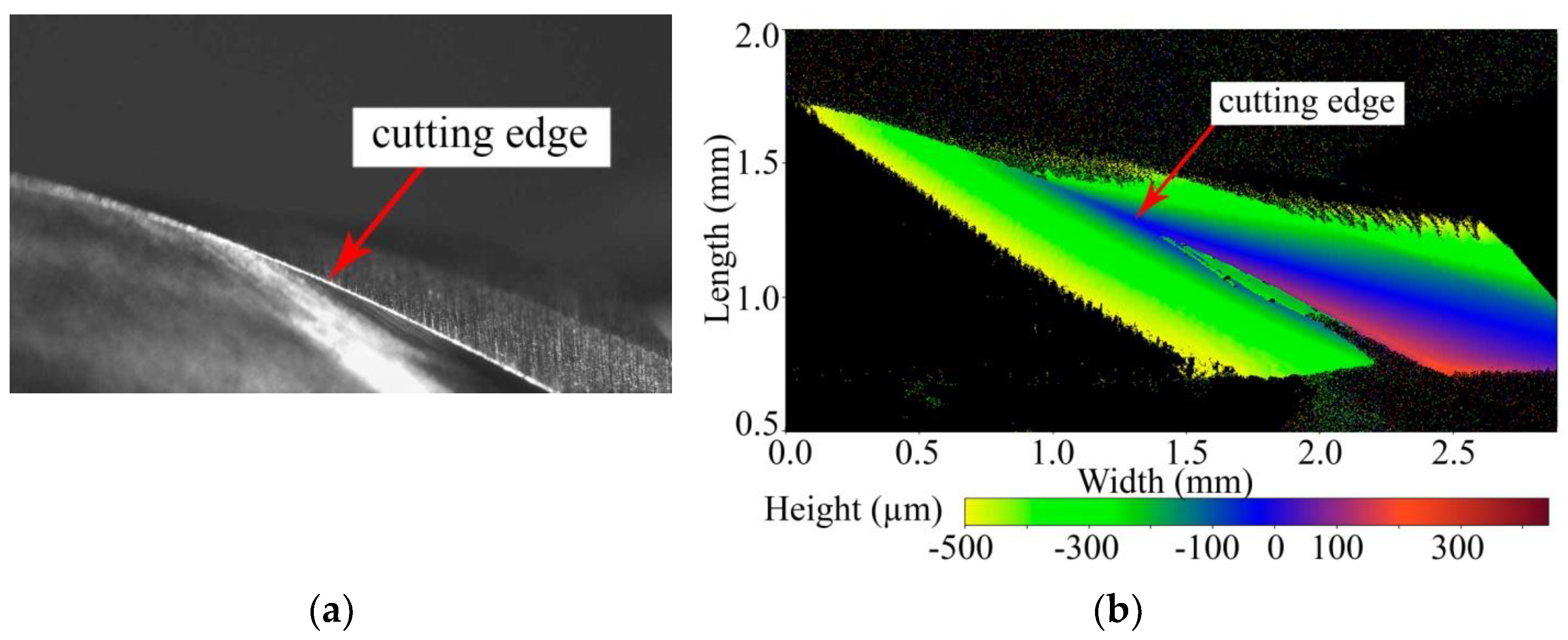
During the measurements, the radius of the cutting edge was estimated in four radial sections distanced from each other at 0.05 mm and distanced from the mill end at 2 mm (Figure 4), 7 mm, or 12 mm.
The radius of the cutting edge was measured in three areas: A, B, and C, which were located from each other with an equal step of 5 mm at a distance of 2, 7, and 12 mm. In each of the areas, the value of the radius r e A , r e B , and r e C is found as the arithmetic mean of the measured values for four sections located at 0.05 mm distance from each other (Equations (1)–(3)).
r e A = r e A 1 + r e A 2 + r e A 3 + + r e A n n
r e B = r e B 1 + r e B 2 + r e B 3 + + r e B n n
r e C = r e C 1 + r e C 2 + r e C 3 + + r e C n n
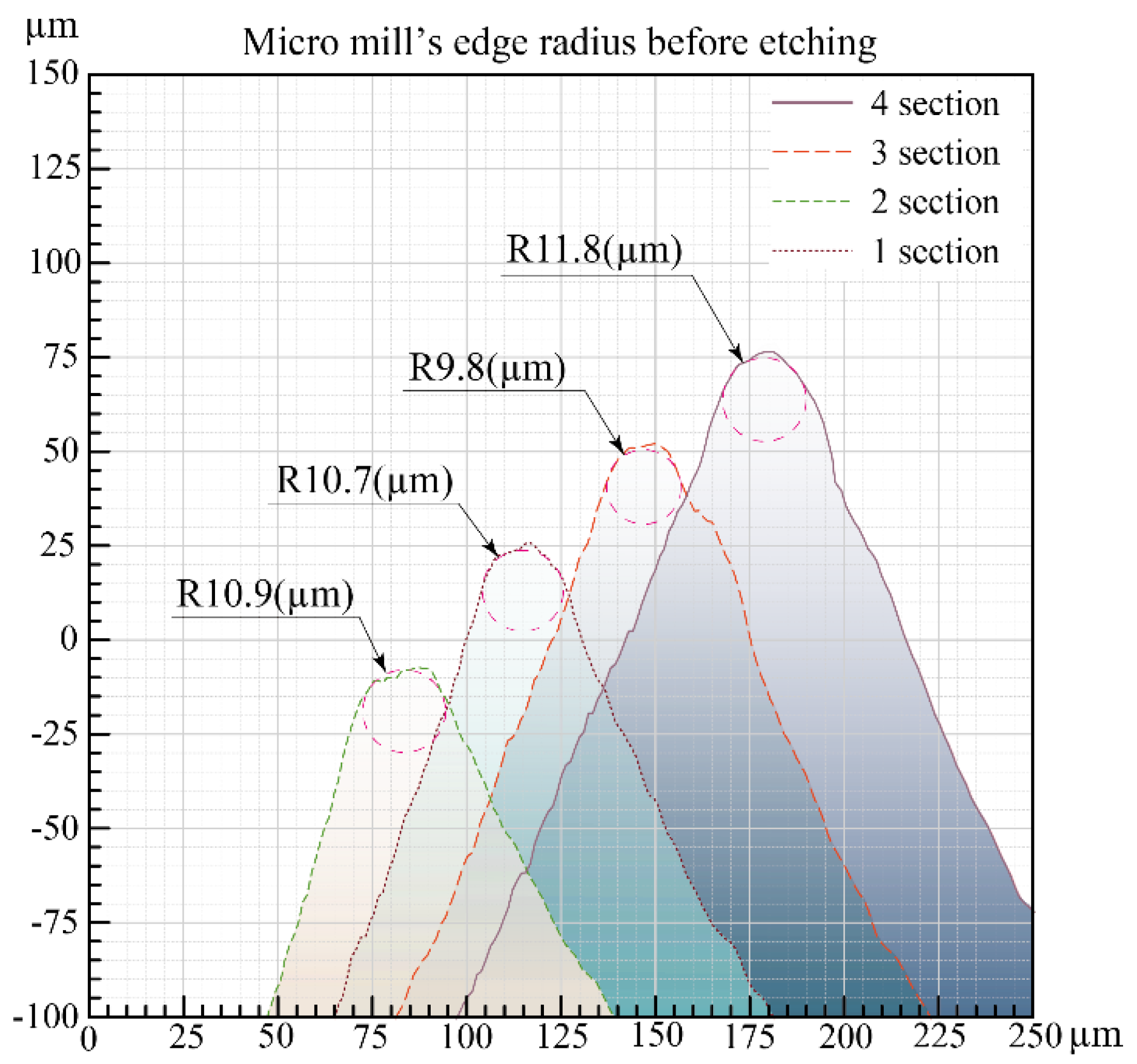
The radius of the cutting edge was measured for the basic type of end mill with grinding clearance and rake surfaces. The average value of the cutting edge radius per 2-mm-distanced area (A) was equal to r e A 10.8 μm (Figure 5); the average value of the cutting edge radius per 7-mm-distanced area (B) was equal to r e B 10.5 μm; and the average value of the cutting edge radius per 12-mm-distanced area (C) was equal to r e C 10.25 μm.
The complete experimental process of the present work comprises:
  • Measurement of cutting edge radii, geometry, and roughness of micro cutters.
  • Etching the micro cutters to reduce their cutting edge radii.
  • Measurement of the cutting edge radii after the etching.
  • Measurement of the geometry and roughness of micro cutters after etching.
  • Deposition of a wear-resistant coating.
  • Final measurement of the cutting edge radii of coated micro cutters.

3. Etching the End Mills with Fast Atoms

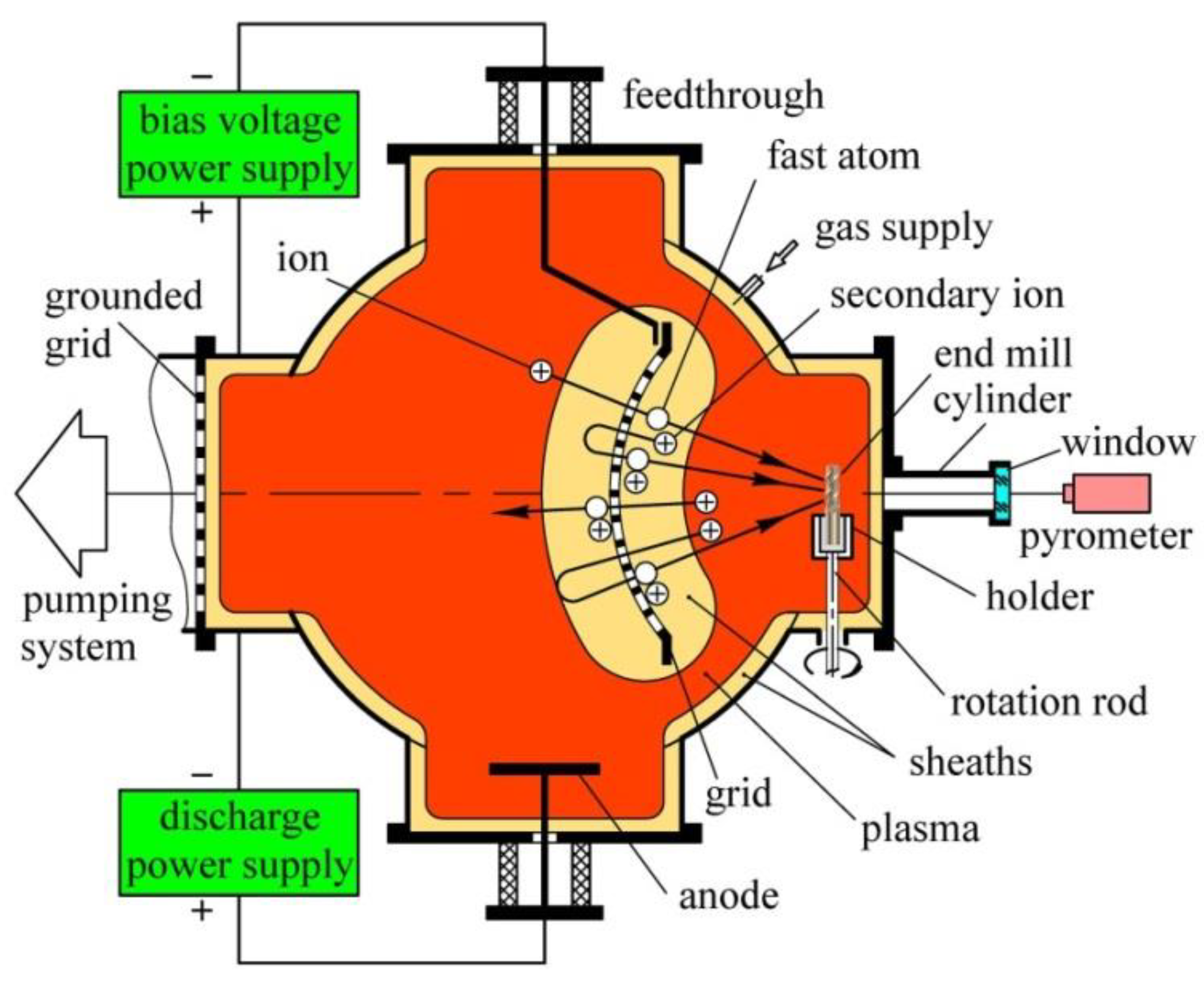
The experimental system for processing the end mills is presented in Figure 6. A 20-cm-diameter concave grid with a surface curvature radius of 20 cm is fixed to the high-voltage feedthrough in the center of the vacuum chamber.
On the grid surface, holes with a diameter of 7 mm are evenly distributed at a distance of 8 mm between their centers. At a distance of 6 cm from the chamber wall is installed a rotating holder for the tools being processed by the beam. The axis of the holder rotation passes through the focal point of the concave grid surface.
At an argon pressure in the chamber p ≈ 0.5 Pa, an increase in the voltage between the anode and the chamber to several hundred volts leads to establishing a gas discharge with a current in the anode circuit Ia up to 4 A and a discharge voltage of Ud = 400–500 V [42]. The chamber is filled with a brightly glowing homogeneous plasma, which is separated from its walls by a cathode sheath and from the grid by a grid sheath of the ion space charge. The sheath width d can be calculated using the derived from the Child–Langmuir law [43] following expression
d = (2/3)εo1/2(2e/M)1/4(U + Ud)3/4/j1/2,
where εo is the electric constant equal to 0.885 × 10⁻¹¹ F/m, e is the electron charge, M is the ion mass, U is the grid bias voltage, and j is the ion current density. When the ion mass M = AMA is measured in atomic mass units A = 1.66 × 10⁻²⁷ kg, the sheath width is equal to
d = 2.34 × 10⁻⁴(MA)−1/4(U + Uc)3/4/j1/2.
When U = 0, the chamber and the grid are equipotential, and both sheaths are of the same width. At p ranging from 0.2 to 1 Pa, the voltage Ud between the chamber and the anode is virtually independent of the argon pressure p at a constant current Ia in the anode circuit. However, at p ˂ 0.2 Pa, a decrease in pressure causes an increase in the discharge voltage Ud, and at p = 0.02 Pa, it reaches a value of Ud ≈ 1 kV. With an increase in the voltage U between the chamber and the grid from zero to 5 kV, the current I in the grid circuit at a constant current Ia in the anode circuit approximately doubles, the width of the sheath d between the plasma and the grid grows to 5–10 cm, and the discharge voltage Ud decreases approximately by two times.
The density of the gas atoms at room temperature and pressure p = 0.02 Pa amounts to n = 0.5 × 10¹⁹ m−3 [44], and the average path of argon ions between charge exchange collisions, called the charge exchange length, is equal to λ = 1/nσ = 1 m. We took into account that for argon ions with an energy of 5 keV, the charge exchange cross-section is equal to σ = 2 × 10⁻¹⁹ m2 [45,46].
At a pressure of p = 0.02 Pa, the width of the grid sheath d ≈ 0.05 m is much lower than the charge exchange length λ, and therefore, no formation of fast atoms in the sheath occurs. All ions extracted from the plasma bombard the grid and cause the emission from its surface of the secondary electrons [47]. Hence, the grid emits only two beams of electrons with energy e(U + Ud), propagating in opposite directions.
With a pressure increase to 0.2 Pa, accelerated ions turn in the sheath into fast atoms escaping from the sheath. The energy of each fast atom, eφ, corresponds to the potential φ of the point in the sheath where it appears. With a pressure increase from 0.2 to 2 Pa, the number of fast atoms increases tenfold, their energy decreases from 5 to 500 eV, and the neutral beam current grows up.
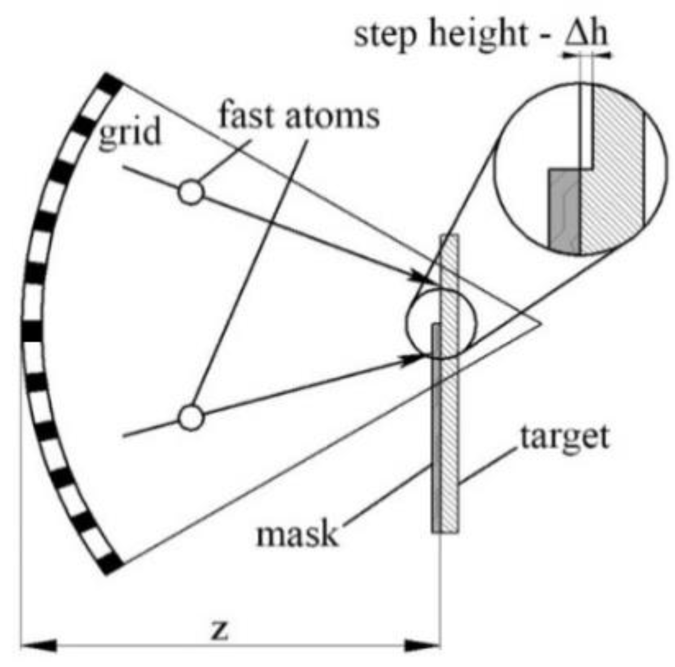
For an estimate of the beam diameter, the distribution of the etching rate by fast atoms of a polished titanium target covered with a mask on its surface was measured. The straight boundary between them is located horizontally (Figure 7). The target was etched with fast atoms, and then, the height of the step between the covered by the mask and open substrate surfaces was measured along the border between them using a mechanical profiler Dektak XT. The etching rate distribution at various distances Z between the target and the grid revealed the beam diameter dependence on Z. As Z increases, the diameter D decreases from 45 mm at Z = 17 cm to 6 mm at Z = 20 cm, and as the distance increases from Z = 21 cm to Z = 24 cm, the diameter D increases from 7 mm up to 52 mm.
Figure 8a presents a photograph of the accelerating grid fastened to the high-voltage feedthrough and the end mill placed on the rotating holder. The grid was distanced at 22 cm from the axis of the rotating holder where the beam diameter amounted to 2 cm. For this reason, the 12-mm-long cutting part of the end mill was etched quite homogeneously by the fast atoms. The beam of fast atoms was generated by the grid immersed in the argon plasma and negatively biased to 5000 V (Figure 8b).
The results of the mills etching are presented in Table 2. They show that at the beginning, for the sections distanced from the mill end at 7 mm, the etching rate is maximum and amounts to 3 μm/h. Further on, the etching rate falls down, and after a 3-h-long etching, it is close to zero for the section distant from the mill end at 7 mm and to 0.2 μm/h for the sections distant from the mill end at 2 and 12 mm.
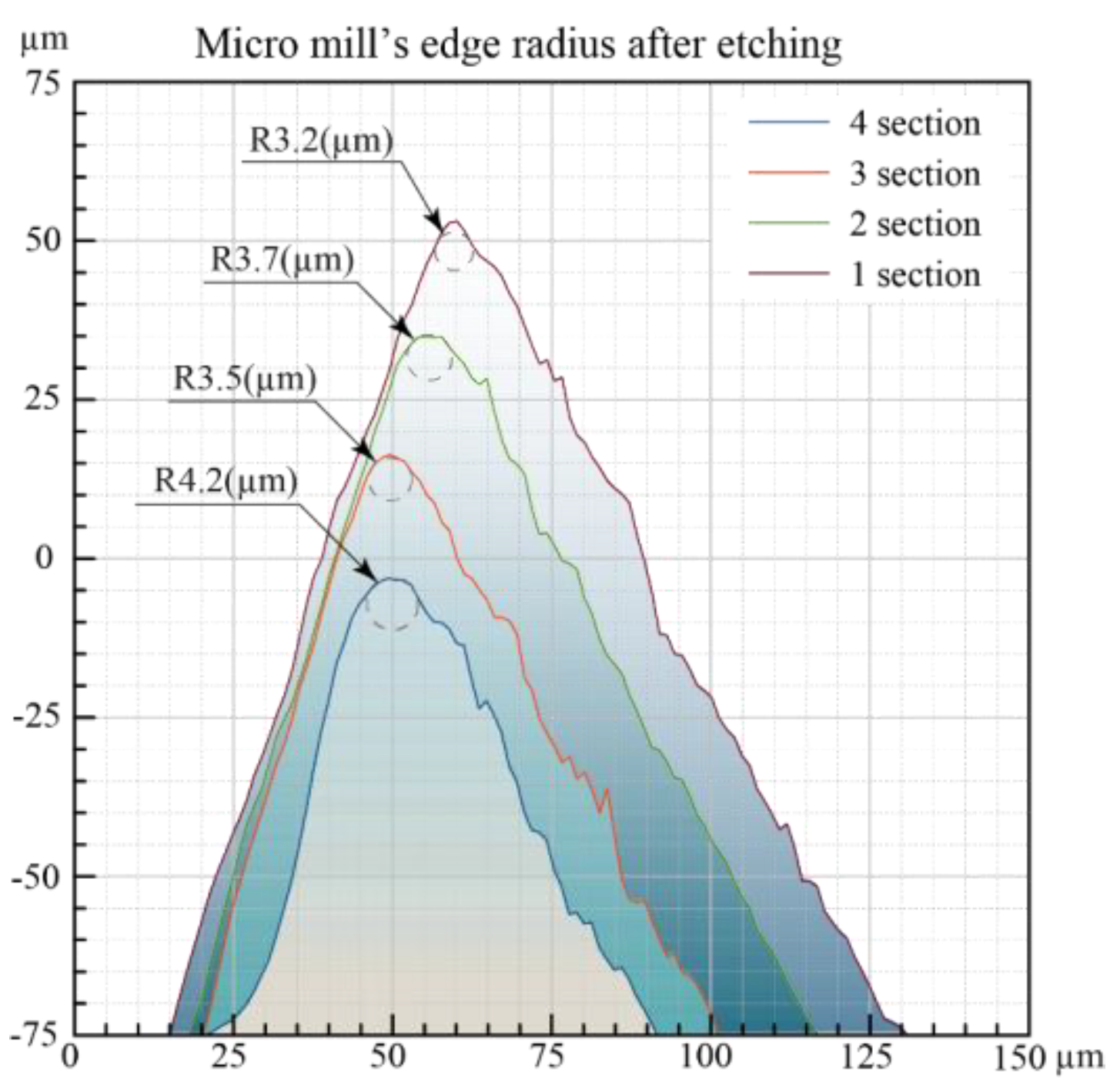
The average value of the cutting edge radius after etching per 2-mm-distanced area (A) was equal to r e A 4.25 μm; the average value of the cutting edge radius per 7-mm-distanced area (B) was equal to r e B 3.65 μm (Figure 9); the average value of the cutting edge radius per 12-mm-distanced area (C) was equal to r e C 4.1 μm.
The analysis of the entire set of measured cutting edge radii showed that the best results were obtained for the 3-h-long etching.
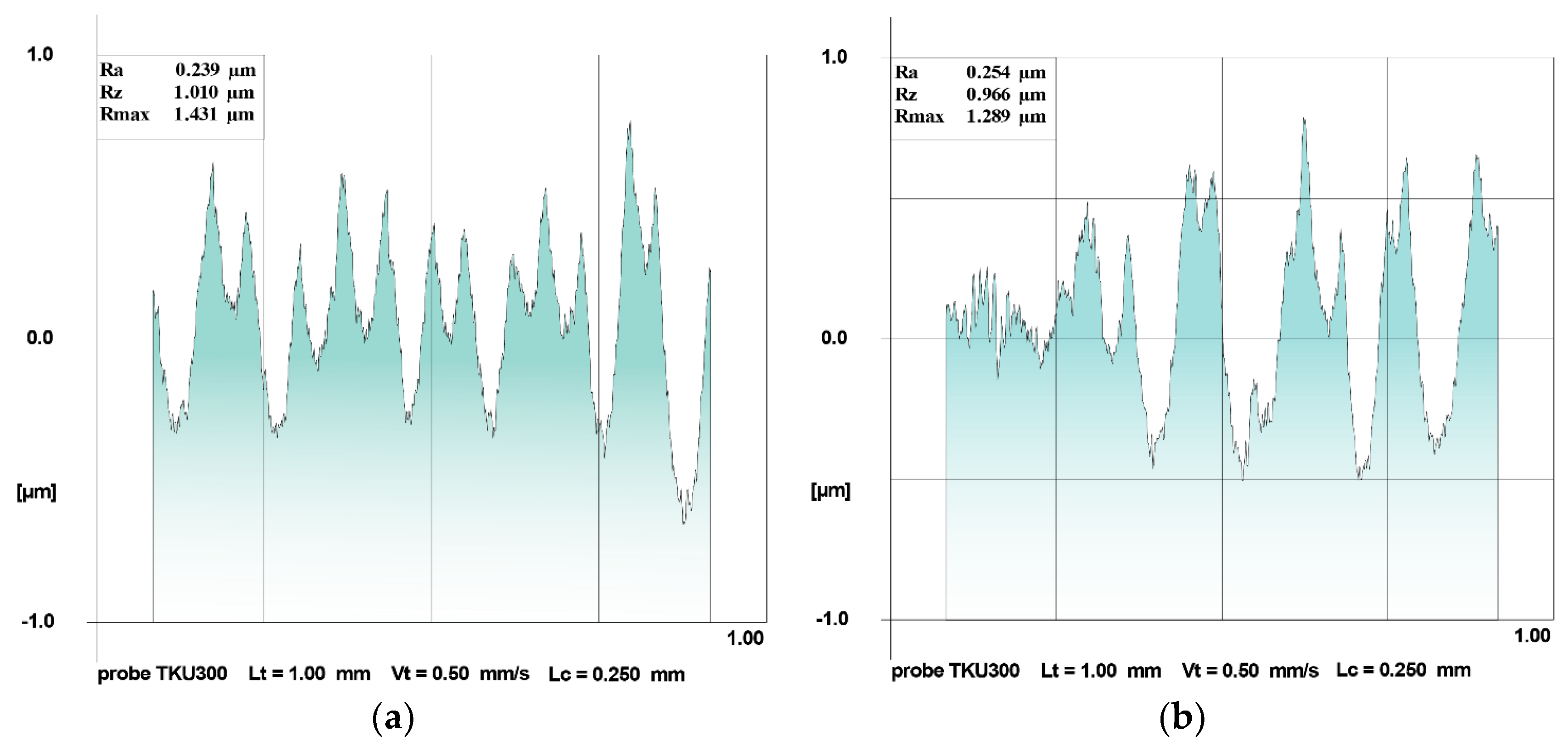
A further increase in the etching time had no benefit for the tool sharpening. It should be mentioned that after quite long etching of the end mills, no significant increase in the surface roughness has been observed (Figure 10).
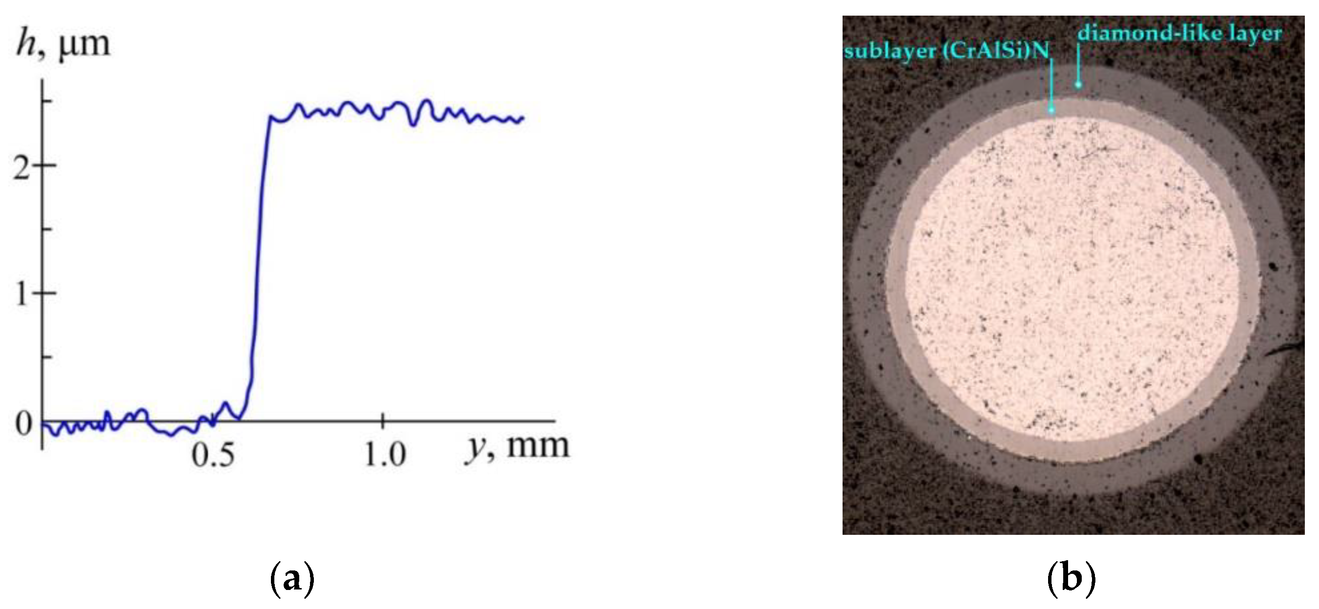
After a 3-h-long etching of the end mill, a wear-resistant coating was synthesized on its surface. The synthesis was carried out according to the standard technology on a Platit π 311 system for the deposition of wear-resistant coatings manufactured by Platit (Switzerland). The deposited diamond-like coating (DLC) was a two-layer composition: an adhesive sublayer based on a complex nitride (CrAlSi)N and an outer wear-resistant DLC layer (Figure 10b). The choice of this particular coating (CrAlSi)N/DLC as an object for research is not accidental. This compound can be used to improve the performance of hard-alloy tools, including small-sized ones. To estimate the thickness of the synthesized coating, a cylindrical mask with an inner diameter of 3 mm was preliminary put on the end mill.
Within an hour, a DLC coating was synthesized on the end mill and its mask. After removing them from the chamber, the mask was detached from the end mill. Using a Dektak XT mechanical profilometer, the height of the step between the coating surface and the end mill surface screened with the mask was measured (Figure 11a). The thickness of the wear-resistant coating synthesized on the end mill is equal to the step height of 2.4 μm.
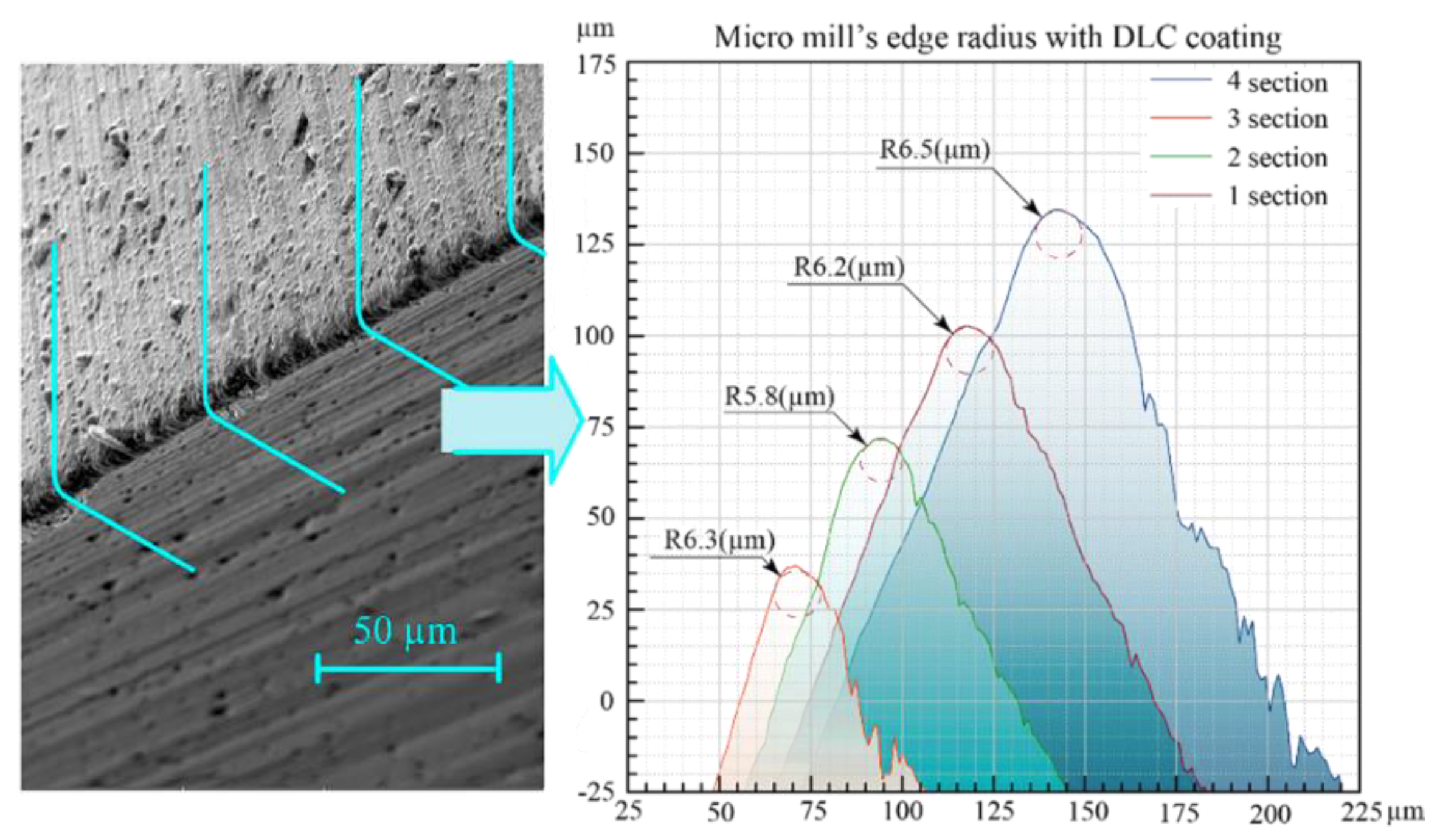
Figure 12 shows the experimentally obtained measurement results, which were performed in four sections of the cutting edge of a 3-mm diameter end mill after a 3-h-long etching and deposition of a two-layer DLC coating. The average value of the cutting edge radii after etching and deposition of a two-layer DLC coating per 2-mm-distanced area (A) was equal to r e A 6.25 μm; the average value of the cutting edge radius per 7-mm-distanced area (B) was equal to r e B 5.5 μm; and the average value of the cutting edge radius per 12-mm-distanced area (C) was equal to r e C 6.2 μm (Figure 12) (Table 3).
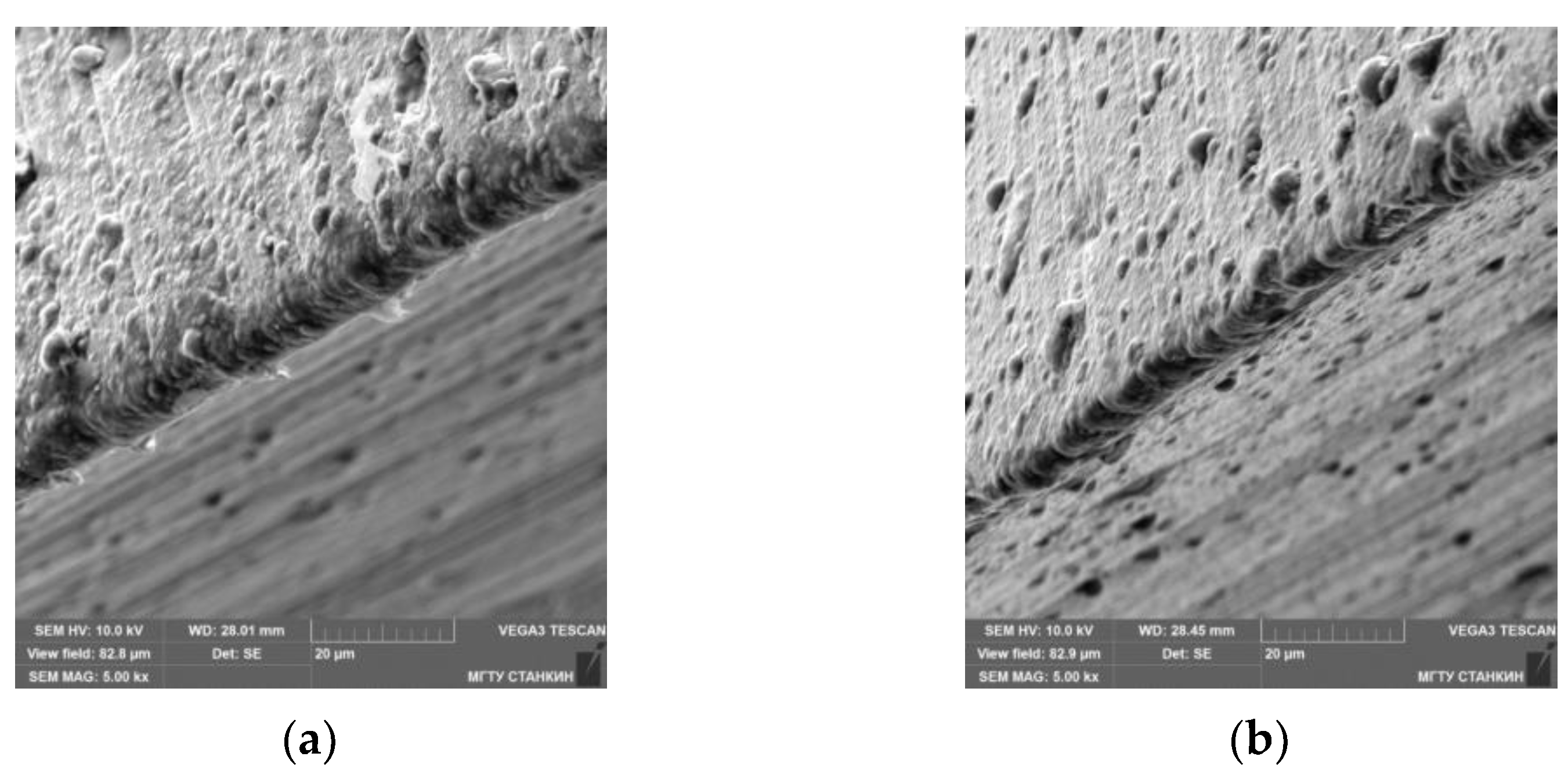
Figure 13 presents SEM images (magnification 5000 times) of the end mill cutting edges after the diamond-like coatings deposition on the end mills sharpened through grinding (a) and by fast argon atoms (b).

4. Discussion

The above results showed that the etching of end mills with a fast atom beam allows an appreciable sharpening of the tools. Due to the etching, the cutting edge radius diminishes to ≈3−4 μm from the minimum value of ≈10−11 μm available with the tool sharpening through grinding. The sharpening occurs due to a quite homogeneous sputtering of the tool surface near the edge at low gas pressure p < 1 Pa. Homogeneous plasma inside the chamber is generated by the glow discharge with a large hollow cathode [48], which is the vacuum chamber itself.
It was discovered in [49] that the lower limit of the glow discharge operating pressure is proportional to the aperture of electron losses from the hollow cathode, and due to a decrease in the aperture, it can be diminished to ≈0.01 Pa. This finding made it possible to use the discharge for the plasma immersion processing of products [50,51], in broad beam sources of gaseous ions [52,53,54,55] and electron beam sources [56,57,58]. The present research is the first attempt to use the discharge for the micro tools processing.
In our case, the aperture of electron losses is equal to the surface area of the anode immersed in the discharge plasma. The volume of the vacuum chamber with a diameter of 50 cm and length of 55 cm amounts to V = 0.12 m3, and its internal surface area is equal to S = 1.5 m2. When the anode area Sa is less than a critical value
S* = (π/e)1/2(2m/M)1/2S ≈ (2m/M)1/2S
where S is the chamber surface area, m and M are the electron mass and the ion mass, and e is the Naperian base, a positive anode fall of potential Ua occurs [42]. With a pressure decrease from 0.1 to 0.01 Pa, the anode fall can grow from Ua ≈ 10 to Ua ≈ 500 V. It results in the anode overheating and melting by electrons accelerated in the negative space charge sheath near the anode surface.
For the discharge in argon and S = 1.5 m2, the critical value amounts to S* = 0.008 m2. Not to have problems with the discharge anode, its surface area was chosen to be equal to Sa = 0.02 m2. This area exceeds the critical anode area of S* = 0.008 m2 and, hence, it prevents the positive anode fall of potential. The discharge plasma uniformity at the gas pressure of 0.01–1 Pa makes it possible to accelerate ions from the main plasma volume in the center of the chamber using a concave grid (Figure 6) and transform the concentrated ion beam into a fast atom beam. The decrease in the cutting edge radius of the end mills after etching with such a beam can be explained in Figure 14.
When a negative voltage is applied to the cutting edge in the plasma, ions are extracted from the plasma and enter the sheath. The width of the sheath at a voltage from 100 to 1000 V exceeds 1 mm. Therefore, the radius of the plasma boundary emitting ions onto the cutting edge surface exceeds about one hundred times the cutting edge radius of 10 μm. In a homogeneous plasma, the ion current density is constant at the entire plasma boundary. However, the area of the plasma emitting ions on the cutting edge is one hundred times larger than the edge area.
Therefore, the ion current density at the edge is a hundred times higher than at the rest of the wedge surface. Etching of the edge leads to a significant increase in its radius, and the tool becomes blunt. To avoid bluntness of the tool, it is necessary to etch not by ions accelerated from the plasma by a voltage applied to the tool but by a broad beam of accelerated ions or fast atoms. They sputter the cutting edge of the tool with the same intensity as the rest of its surface. When removing a surface layer of the same thickness, the radius of the cutting edge decreases. Therefore, the tool is sharpened, when it is etched by a broad beam.
In our experiments, the cutting edge radius diminished to ≈3−4 μm from the minimum value of ≈10−11 μm available at the tool sharpening through grinding. In the beginning, the etching rate amounted to ≈2 μm/h, and after a 3-h-long etching, it diminished to zero. The reason for this phenomenon can be related to the structure of the end mill material. In our case, it was a carbide type HM CK10-20-MG Micrograin of carbide group: tungsten-cobalt single-corpus with the carbide grain size of 0.8 μm. One can hardly imagine a tool with a cutting edge radius of ≈1 μm made of a material with a grain size of 0.8 μm. In our experiments, the minimum cutting edge radius exceeds the grain size by five times.
The results of the end mills etching presented in Table 2 exhibit another specific feature to be explained. They reveal a difference in the dependencies on the etching time of the cutting edge radius for the end mill sections distant from the mill end at 2, 7, and 12 mm. The 12-mm-long cutting part of the end mill rotated in the center of the 20-mm-diameter beam and should be etched quite homogeneously. Nevertheless, the etching rate for the section distant from the mill end at 7 mm was a little higher than for the sections distant from the mill end at 2 and 12 mm. It could be caused by a radial distribution of the fast atom flow density with a maximum at the beam axis.
The use of wear-resistant coatings prevents the intensive wear of the cutting tool; however, the coating affects the microgeometry of the cutting edge by increasing the radius of its rounding. With an increase in the radius of the cutting edge about the thickness of the cut layer, the deformation area of the workpiece increases, and as a result, the force load on the tool tooth increases [31]. Cutting forces have a great influence on the chip formation nature, the process of material cutting, vibration characteristics of cutting, the integrity of the cutting tool, and the surface quality [59,60,61,62]. Additional surface treatment by fast atoms will reduce the cutting edge radius and prepare surfaces for the deposition of a wear-resistant coating while providing a relatively smaller radius of the cutting edge than when coating the surface without preparation of this kind.
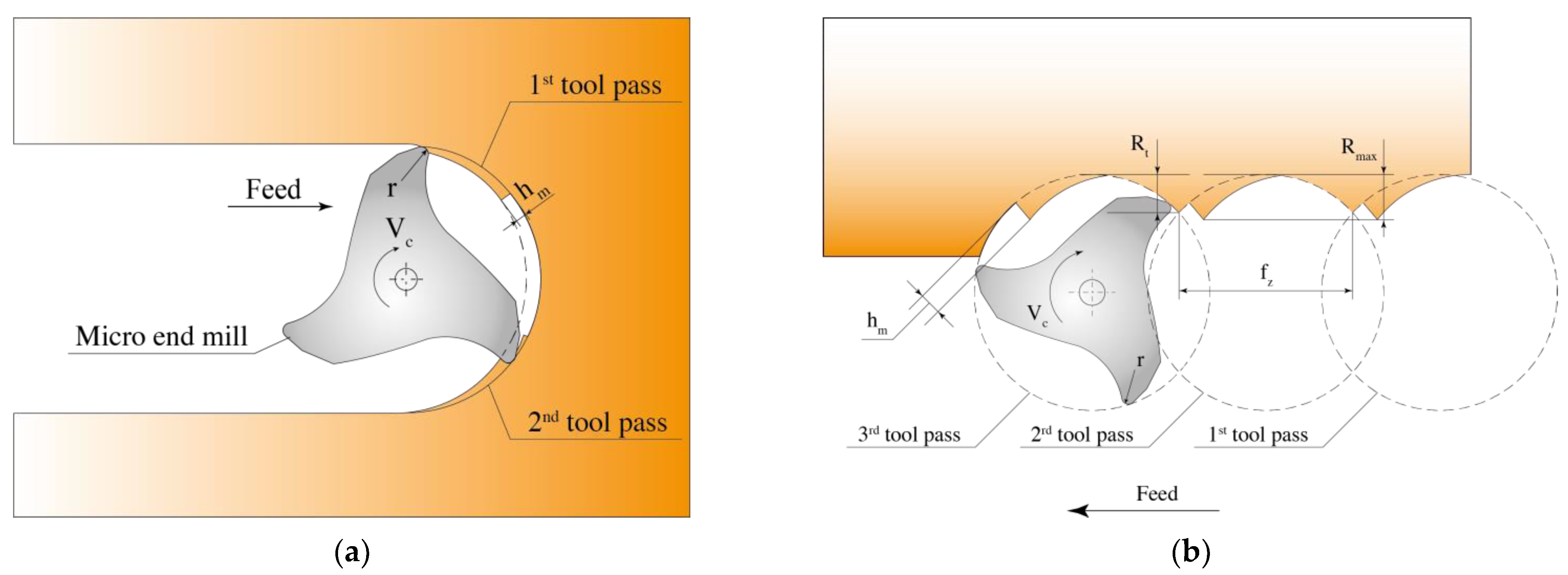
Unlike the constant undeformed chip thickness (UCT) and direction of cutting speed in orthogonal micro-cutting, both vary in a time-dependent manner in micro-milling. The micro-milling process can be considered as the composition of varied orthogonal micro-cutting in the time domain [63,64,65]. In end micro-milling (Figure 15a), the thickness (i) initially increases from zero, (ii) reaches the maximum value (approximately equal to the feed per tooth), and (iii) reduces to zero, while in a side micro-milling (Figure 15b), the thickness decreases from maximum to zero. The above stages may occur sequentially for a single cutting edge, or, in most common scenarios, simultaneously for multiple cutting edges depending on the employed tool geometries (the cutting edge radius and tooth number) and the machining parameter (feed per tooth) [66]. This would result in very complex material behaviors in comparison with orthogonal micro-cutting.
Consider the side micro-milling process based on the two-tooth micro milling cutter as an example. If the UCT at the entrance is larger than the minimum undeformed chip thickness (MUCT), the chip begins to form (Figure 15b). However, when the instantaneous UCT becomes smaller than the MUCT, the chip generation would stop. A part of the workpiece material will elastically recover, while other material will undergo plastic deformation after the micro-milling cutter is passed by. The machined surface in a side micro-milling includes both the theoretical residual height (Rt) and the residual height (Rmax) left by the existing MUCT (Figure 16b) [62]. Rmax in micro-milling can be expressed as Equation (7) [62], respectively, and they are primarily related to the feed per tooth (fz) and MUCT (hm), as shown in Equation (8).
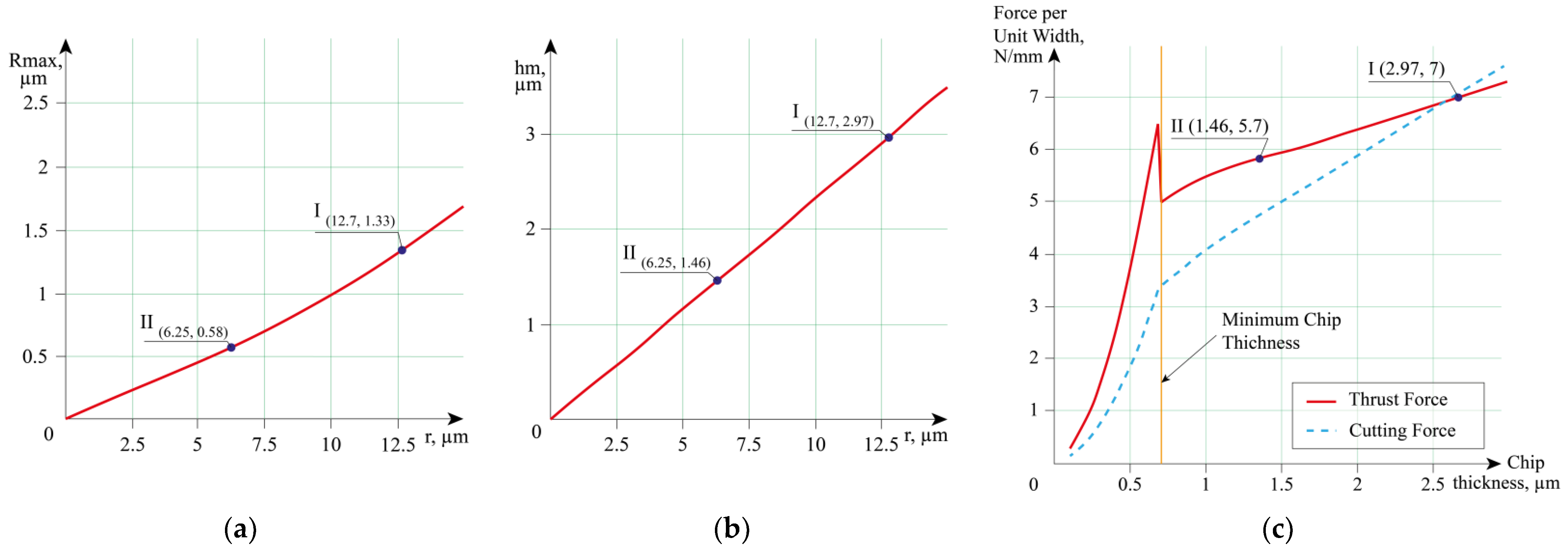
As a result of using the etching operation before coating, the radius of the cutting edge can be reduced to 6.25 microns compared to 12.7 after coating a ground micro mill.
Reducing the cutting edge radius allows decreasing the height of residual microroughness formed during cutting in the area of the plunger zone from 1.33 μm (point I in Figure 16a) to 0.58 μm (point II in Figure 16a), minimum undeformed chip thickness hm from 2.97 μm (point I in Figure 16b) to 1.46 μm (point II in Figure 16b), forces in the ploughing-dominated region determined on the base of ref. [65,66] from 7 N/mm (point I in Figure 16c) to 5.7 N/mm (point II in Figure 16c) when machining a steel part with the following parameters β 40°, Poisson’s ratio k 0.25 (for steel), mill’s radius Rf 1.5 mm, feed per tooth 0.005 mm/tooth. After the chip thickness of 3.0 μm, where the effect of ploughing becomes small and that of shearing is more significant, forces for pearlite became higher, but increasing these parameters are actual only for the machining process with small deps of cut [67,68,69].
R max = f z 2 8 R f + ( 1 k ) h m 2 ( 1 + [ ( 1 k ) h m ] 2 f z 2 )
  h m = r ( 1 cos ( β ) )

5. Conclusions

  • The etching of micro tools with a concentrated beam of fast atoms allows an appreciable sharpening of the tools. Due to the etching, the cutting edge radius diminishes to ≈3−4 μm from the minimum value of ≈10−11 μm available at the tool sharpening through grinding.
  • The sharpening of micro tools with a fast atom beam makes it possible to avoid blunting of their cutting edges caused by an increase in their radii after the coating deposition.
  • The new method of cutting tool processing improves the cutting conditions and property of the cutting wedge.

Author Contributions

Conceptualization, A.M. and P.P.; methodology, A.M. and P.P.; software, I.M. and E.M.; validation, A.M., P.P. and Y.M.; formal analysis, Y.M.; investigation, Y.M. and I.M.; resources, Y.M., I.M. and E.M.; data curation, P.P., Y.M. and I.M.; writing—original draft preparation, A.M. and P.P.; writing—review and editing, A.M.; visualization, I.M.; supervision, A.M.; project administration, P.P.; funding acquisition, A.M. All authors have read and agreed to the published version of the manuscript.

Funding

This work is funded by the state assignment of the Ministry of Science and Higher Education of the Russian Federation, project No. 0707-2020-0025.

Institutional Review Board Statement

Not applicable.

Informed Consent Statement

Not applicable.

Data Availability Statement

Not applicable.

Acknowledgments

The work was carried out using the equipment of the Center of collective use of “MSUT “STANKIN”.

Conflicts of Interest

The authors declare no conflict of interest.

References

  1. Grigoriev, S.; Metel, A. Plasma- and Beam-Assisted Deposition Methods; Nato Science Series, Series Ii: Mathematics, Physics and Chemistry; Nanostructured Thin Films and Nanodispersion Strengthened Coatings. In NATO Science Series II: Mathematics, Physics and Chemistry; Voevodin, A.A., Shtansky, D.V., Levashov, E.A., Moore, J.J., Eds.; Springer: Dordrecht, The Netherlands, 2004; Volume 155, pp. 147–154. [Google Scholar] [CrossRef]
  2. Sobol’, O.V.; Andreev, A.A.; Grigoriev, S.N.; Gorban’, V.F.; Volosova, M.A.; Aleshin, S.V.; Stolbovoy, V.A. Physical char-acteristics, structure and stress state of vacuum-arc TiN coating, deposition on the substrate when applying high-voltage pulse during the deposition. Probl. Atom. Sci. Technol. 2011, 4, 174–177. [Google Scholar]
  3. Zhitomirsky, V.; Grimberg, I.; Rapoport, L.; Boxman, R.; Travitzky, N.; Goldsmith, S.; Weiss, B. Bias voltage and incidence angle effects on the structure and properties of vacuum arc deposited TiN coatings. Surf. Coat. Technol. 2000, 133–134, 114–120. [Google Scholar] [CrossRef]
  4. Musil, J. High-rate magnetron sputtering. J. Vac. Sci. Technol. A 1996, 14, 2187–2191. [Google Scholar] [CrossRef]
  5. Boxman, R.L.; Zhitomirsky, V.N. Vacuum arc deposition devices. Rev. Sci. Instrum. 2006, 77, 021101. [Google Scholar] [CrossRef]
  6. Musil, J.; Leština, J.; Vlček, J.; Tölg, T. Pulsed dc magnetron discharge for high-rate sputtering of thin films. J. Vac. Sci. Technol. A 2001, 19, 420–424. [Google Scholar] [CrossRef]
  7. Horwat, D.; Anders, A. Spatial distribution of average charge state and deposition rate in high power impulse magnetron sputtering of copper. J. Phys. D Appl. Phys. 2008, 41, 135210. [Google Scholar] [CrossRef] [Green Version]
  8. Oks, E.; Anders, A. Evolution of the plasma composition of a high power impulse magnetron sputtering system studied with a time-of-flight spectrometer. J. Appl. Phys. 2009, 105, 093304. [Google Scholar] [CrossRef] [Green Version]
  9. Anders, A. Discharge physics of high power impulse magnetron sputtering. Surf. Coat. Technol. 2011, 205, S1–S9. [Google Scholar] [CrossRef] [Green Version]
  10. Greczynski, G.; Hultman, L. Time and energy resolved ion mass spectroscopy studies of the ion flux during high power pulsed magnetron sputtering of Cr in Ar and Ar/N2 atmospheres. Vacuum 2010, 84, 1159–1170. [Google Scholar] [CrossRef] [Green Version]
  11. Sarakinos, K.; Alami, J.; Konstantinidis, S. High power pulsed magnetron sputtering: A review on scientific and engineering state of the art. Surf. Coat. Technol. 2010, 204, 1661–1684. [Google Scholar] [CrossRef]
  12. Hala, M.; Viau, N.; Zabeida, O.; Klemberg-Sapieha, J.E.; Martinu, L. Dynamics of reactive high-power impulse magnetron sputtering discharge studied by time- and space-resolved optical emission spectroscopy and fast imaging. J. Appl. Phys. 2010, 107, 043305. [Google Scholar] [CrossRef]
  13. Musil, J.; Baroch, P. High-rate pulsed reactive magnetron sputtering of oxide nanocomposite coatings. Vacuum 2013, 87, 96–102. [Google Scholar] [CrossRef]
  14. Metel, A.S.; Bolbukov, V.P.; Volosova, M.A.; Grigoriev, S.N.; Melnik, Y.A. Equipment for deposition of thin metallic films bombarded by fast argon atoms. Instrum. Exp. Tech. 2014, 57, 345–351. [Google Scholar] [CrossRef]
  15. Boxman, R.; Zhitomirsky, V.; Alterkop, B.; Gidalevich, E.; Beilis, I.; Keidar, M.; Goldsmith, S. Recent progress in filtered vacuum arc deposition. Surf. Coat. Technol. 1996, 86–87, 243–253. [Google Scholar] [CrossRef]
  16. Aksenov, I.I.; Aksyonov, D.S. Vacuum arc plasma source with rectilinear filter for deposition of functional coatings. Funct. Mater. 2008, 15, 442–447. Available online: https://scholar.google.com/scholar?q=Vacuum%20arc%20plasma%20source%20with%20rectilinear%20filter%20for%20deposition%20of%20functional%20coatings (accessed on 14 April 2021).
  17. Anders, A.; Pasaja, N.; Sansongsiri, S. Filtered cathodic arc deposition with ion-species-selective bias. Rev. Sci. Instrum. 2007, 78, 063901. [Google Scholar] [CrossRef] [Green Version]
  18. Kleiman, A.; Márquez, A.; Boxman, R.L. Performance of a magnetic island macroparticle filter in a titanium vacuum arc. Plasma Sources Sci. Technol. 2007, 17, 015008. [Google Scholar] [CrossRef]
  19. Sanginés, R.; Bilek, M.M.M.; McKenzie, D.R. Optimizing filter efficiency in pulsed cathodic vacuum arcs operating at high currents. Plasma Sources Sci. Technol. 2009, 18, 045007. [Google Scholar] [CrossRef]
  20. Sato, A.; Iwao, T.; Yumoto, M. Relation between surface roughness and number of cathode spots of a low-pressure arc. Plasma Sources Sci. Technol. 2008, 17, 045007. [Google Scholar] [CrossRef]
  21. Rysanek, F.; Burton, R.L. Charging of Macroparticles in a Pulsed Vacuum Arc Discharge. IEEE Trans. Plasma Sci. 2008, 36, 2147–2162. [Google Scholar] [CrossRef]
  22. Ehiasarian, A.P.; Anders, A.; Petrov, I. Combined filtered cathodic arc etching pretreatment–magnetron sputter deposition of highly adherent CrN films. J. Vac. Sci. Technol. A 2007, 25, 543–550. [Google Scholar] [CrossRef]
  23. Metel, A.S.; Bolbukov, V.P.; Volosova, M.A.; Grigoriev, S.N.; Melnik, Y.A. Source of metal atoms and fast gas molecules for coating deposition on complex shaped dielectric products. Surf. Coat. Technol. 2013, 225, 34–39. [Google Scholar] [CrossRef]
  24. Ruset, C.; Grigore, E. The influence of ion implantation on the properties of titanium nitride layer deposited by magnetron sputtering. Surf. Coat. Technol. 2002, 156, 159–161. [Google Scholar] [CrossRef]
  25. Ruset, C.; Grigore, E.; Collins, G.; Short, K.; Rossi, F.; Gibson, N.; Dong, H.; Bell, T. Characteristics of the Ti2N layer produced by an ion assisted deposition method. Surf. Coat. Technol. 2003, 174–175, 698–703. [Google Scholar] [CrossRef]
  26. Grigore, E.; Ruset, C.; Short, K.T.; Hoeft, D.; Dong, H.; Li, X.Y.; Bell, T. In situ investigation of the internal stress within the nc-Ti2N/nc-TiN nanocomposite coatings produced by a combined magnetron sputtering and ion implantation method. Surf. Coat. Technol. 2005, 200, 744–747. [Google Scholar] [CrossRef]
  27. Uhlmann, E.; Oberschmidt, D.; Kuche, Y.; Löwenstein, A. Cutting Edge Preparation of Micro Milling Tools. Procedia CIRP 2014, 14, 349–354. [Google Scholar] [CrossRef]
  28. Aurich, J.C.; Bohley, M.; Reichenbach, I.G.; Kirsch, B. Surface quality in micro milling: Influences of spindle and cutting parameters. CIRP Ann. 2017, 66, 101–104. [Google Scholar] [CrossRef]
  29. Dib, M.; Duduch, J.; Jasinevicius, R. Minimum chip thickness determination by means of cutting force signal in micro endmilling. Precis. Eng. 2018, 51, 244–262. [Google Scholar] [CrossRef]
  30. Biermann, D.; Baschin, A. Influence of cutting edge geometry and cutting edge radius on the stability of micromilling processes. Prod. Eng. 2009, 3, 375–380. [Google Scholar] [CrossRef]
  31. Wojciechowski, S.; Matuszak, M.; Powałka, B.; Madajewski, M.; Maruda, R.; Królczyk, G. Prediction of cutting forces during micro end milling considering chip thickness accumulation. Int. J. Mach. Tools Manuf. 2019, 147, 103466. [Google Scholar] [CrossRef]
  32. Mian, A.J.; Driver, N.; Mativenga, P.T. Identification of factors that dominate size effect in micro-machining. Int. J. Mach. Tools Manuf. 2011, 51, 383–394. [Google Scholar] [CrossRef]
  33. Volosova, M.A.; Grigor’Ev, S.N.; Kuzin, V.V. Effect of Titanium Nitride Coating on Stress Structural Inhomogeneity in Oxide-Carbide Ceramic. Part 4. Action of Heat Flow. Refract. Ind. Ceram. 2015, 56, 91–96. [Google Scholar] [CrossRef]
  34. Grigoriev, S.N.; Sobol, O.V.; Beresnev, V.M.; Serdyuk, I.V.; Pogrebnyak, A.D.; Kolesnikov, D.A.; Nemchenko, U.S. Tribological characteristics of (TiZrHfVNbTa) N coatings applied using the vacuum arc deposition method. J. Frict. Wear 2014, 35, 359–364. [Google Scholar] [CrossRef]
  35. Kuzin, V.V.; Grigoriev, S.N.; Fedorov, M.Y. Role of the thermal factor in the wear mechanism of ceramic tools. Part 2: Microlevel. J. Frict. Wear 2015, 36, 40–44. [Google Scholar] [CrossRef]
  36. Kuzin, V.V.; Grigor’Ev, S.N.; Volosova, M.A. Effect of a TiC Coating on the Stress-Strain State of a Plate of a High-Density Nitride Ceramic Under Nonsteady Thermoelastic Conditions. Refract. Ind. Ceram. 2014, 54, 376–380. [Google Scholar] [CrossRef]
  37. Lee, S.W.; Choi, H.J.; Lee, H.W.; Choi, J.Y.; Jeong, H.D. A Study of Micro-Tool Machining Using Electrolytic In-Process Dressing and an Evaluation of its Characteristics. Key Eng. Mater. 2003, 238–239, 35–42. [Google Scholar] [CrossRef]
  38. Grigoriev, S.N.; Melnik, Y.A.; Metel, A.S.; Panin, V.V. Broad beam source of fast atoms produced as a result of charge exchange collisions of ions accelerated between two plasmas. Instrum. Exp. Tech. 2009, 52, 602–608. [Google Scholar] [CrossRef]
  39. Metel, A.S.; Grigoriev, S.N.; Melnik, Y.A.; Bolbukov, V.P. Broad beam sources of fast molecules with segmented cold cathodes and emissive grids. Instrum. Exp. Tech. 2012, 55, 122–130. [Google Scholar] [CrossRef]
  40. Metel, A.S.; Grigoriev, S.N.; Melnik, Y.A.; Bolbukov, V.P. Characteristics of a fast neutral atom source with electrons injected into the source through its emissive grid from the vacuum chamber. Instrum. Exp. Tech. 2012, 55, 288–293. [Google Scholar] [CrossRef]
  41. Metel, A.; Grigoriev, S.; Melnik, Y.; Panin, V.; Prudnikov, V. Cutting Tools Nitriding in Plasma Produced by a Fast Neutral Molecule Beam. Jpn. J. Appl. Phys. 2011, 50, 08JG04. [Google Scholar] [CrossRef]
  42. Metel, A.S.; Grigoriev, S.N.; Melnik, Y.A.; Prudnikov, V.V. Glow discharge with electrostatic confinement of electrons in a chamber bombarded by fast electrons. Plasma Phys. Rep. 2011, 37, 628–637. [Google Scholar] [CrossRef]
  43. Langmuir, I. The Interaction of Electron and Positive Ion Space Charges in Cathode Sheaths. Phys. Rev. 1929, 33, 954–989. [Google Scholar] [CrossRef]
  44. McDaniel, E.W. Collision Phenomena in Ionized Gases; Willey: New York, NY, USA, 1964; Available online: https://scholar.google.com/scholar_lookup?title=Collision+Phenomena+in+Ionized+Gases&author=McDaniel,+E.W.&publication_year=1964 (accessed on 14 April 2021).
  45. Phelps, A.V. Cross Sections and Swarm Coefficients for Nitrogen Ions and Neutrals in N2 and Argon Ions and Neutrals in Ar for Energies from 0.1 eV to 10 keV. J. Phys. Chem. Ref. Data 1991, 20, 557–573. [Google Scholar] [CrossRef]
  46. Phelps, A.V.; Greene, C.H.; Burke, J.P. Collision cross sections for argon atoms with argon atoms for energies from 0.01 eV to 10 keV. J. Phys. B At. Mol. Opt. Phys. 2000, 33, 2965–2981. [Google Scholar] [CrossRef]
  47. Kaminsky, M. Atomic and Ionic Impact Phenomena on Metal. Surfaces; Springer: Berlin, Germany, 1965; Available online: https://scholar.google.com/scholar_lookup?title=Atomic+and+Ionic+Impact+Phenomena+on+Metal+Surfaces&author=Kaminsky,+M.&publication_year=1965 (accessed on 14 April 2021).
  48. Korolev, Y.D.; Koval, N.N. Low-pressure discharges with hollow cathode and hollow anode and their applications. J. Phys. D Appl. Phys. 2018, 51, 323001. [Google Scholar] [CrossRef]
  49. Metel, A. Ionization effect in cathode layers on glow-discharge characteristics with oscillating electrons.1. Discharge with the hollow-cathode. Zhurnal Tekhnicheskoi Fiz. 1985, 55, 1928–1934. [Google Scholar]
  50. Koval, N.; Ryabchikov, A.; Sivin, D.; Lopatin, I.; Krysina, O.; Akhmadeev, Y.; Ignatov, D. Low-energy high-current plasma immersion implantation of nitrogen ions in plasma of non-self-sustained arc discharge with thermionic and hollow cathodes. Surf. Coat. Technol. 2018, 340, 152–158. [Google Scholar] [CrossRef]
  51. Gavrilov, N.V.; Mamaev, A.S.; Chukin, A.V. Nitriding of Stainless Steel in Electron-Beam Plasma in the Pulsed and DC Generation Modes. J. Surf. Investig. X ray Synchrotron Neutron Tech. 2017, 11, 1167–1172. [Google Scholar] [CrossRef]
  52. Gavrilov, N.V. New broad beam gas ion source for industrial application. J. Vac. Sci. Technol. A 1996, 14, 1050–1055. [Google Scholar] [CrossRef]
  53. Gavrilov, N.; Mesyats, G.; Radkovski, G.; Bersenev, V. Development of technological sources of gas ions on the basis of hollow-cathode glow discharges. Surf. Coat. Technol. 1997, 96, 81–88. [Google Scholar] [CrossRef]
  54. Oks, E.M.; Vizir, A.V.; Yushkov, G.Y. Low-pressure hollow-cathode glow discharge plasma for broad beam gaseous ion source. Rev. Sci. Instrum. 1998, 69, 853–855. [Google Scholar] [CrossRef]
  55. Vizir, A.V.; Yushkov, G.Y.; Oks, E.M. Further development of a gaseous ion source based on low-pressure hollow cathode glow. Rev. Sci. Instrum. 2000, 71, 728–730. [Google Scholar] [CrossRef]
  56. Favre, M.; Chuaqui, H.; Wyndham, E.; Choi, P. Measurements on electron beams in pulsed hollow-cathode discharges. IEEE Trans. Plasma Sci. 1992, 20, 53–56. [Google Scholar] [CrossRef]
  57. Larigaldie, S.; Caillault, L. Dynamics of a helium plasma sheet created by a hollow-cathode electron beam. J. Phys. D Appl. Phys. 2000, 33, 3190–3197. [Google Scholar] [CrossRef]
  58. Gleizer, J.Z.; Krokhmal, A.; Krasik, Y.E.; Felsteiner, J. High-current electron beam generation by a pulsed hollow cathode. J. Appl. Phys. 2002, 91, 3431–3443. [Google Scholar] [CrossRef]
  59. Son, S.M.; Han, S.L.; Ahn, J.H. Effects of the friction coefficient on the minimum cutting thickness in micro cutting. Int. J. Mach. Tools Manuf. 2005, 45, 535. [Google Scholar] [CrossRef]
  60. Balázs, B.Z.; Geier, N.; Takács, M.; Davim, J.P. A review on micro-milling: Recent advances and future trends. Int. J. Adv. Manuf. Technol. 2021, 112, 655–684. [Google Scholar] [CrossRef]
  61. O’Toole, L.; Kang, C.-W.; Fang, F.-Z. Precision micro-milling process: State of the art. Adv. Manuf. 2020, 1–33. [Google Scholar] [CrossRef]
  62. Davoudinejad, A.; Tosello, G.; Parenti, P.; Annoni, M. 3D Finite Element Simulation of Micro End-Milling by Considering the Effect of Tool Run-Out. Micromachines 2017, 8, 187. [Google Scholar] [CrossRef] [Green Version]
  63. Chen, N.; Li, H.N.; Wu, J.; Li, Z.; Li, L.; Liu, G.; He, N. Advances in micro milling: From tool fabrication to process outcomes. Int. J. Mach. Tools Manuf. 2021, 160, 103670. [Google Scholar] [CrossRef]
  64. Weule, H.; Hüntrup, V.; Tritschler, H. Micro-Cutting of Steel to Meet New Requirements in Miniaturization. CIRP Ann. 2001, 50, 61–64. [Google Scholar] [CrossRef]
  65. Jun, M.B.G.; Devor, R.E.; Kapoor, S.G. Investigation of the Dynamics of Microend Milling—Part II: Model Validation and Interpretation. J. Manuf. Sci. Eng. 2006, 128, 901–912. [Google Scholar] [CrossRef]
  66. Zhang, X.; Ehmann, K.F.; Yu, T.; Wang, W. Cutting forces in micro end milling processes. Int. J. Mach. Tool Manuf. 2016, 107, 21–40. [Google Scholar] [CrossRef]
  67. Vereschaka, A.; Grigoriev, S.; Popov, A.; Batako, A. Nano-scale Multilayered Composite Coatings for Cutting Tools Operating under Heavy Cutting Conditions. Procedia CIRP 2014, 14, 239–244. [Google Scholar] [CrossRef] [Green Version]
  68. Fominski, V.; Grigoriev, S.; Gnedovets, A.; Romanov, R. Pulsed laser deposition of composite Mo-Se-Ni-C coatings using standard and shadow mask configuration. Surf. Coat. Technol. 2012, 206, 5046–5054. [Google Scholar] [CrossRef]
  69. Vereschaka, A.; Volosova, M.; Grigoriev, S. Development of Wear-resistant Complex for High-speed Steel Tool when Using Process of Combined Cathodic Vacuum Arc Deposition. Procedia CIRP 2013, 9, 8–12. [Google Scholar] [CrossRef] [Green Version]
Figure 1. Photograph of a 3-mm-diameter end mill with a 30-degree angle of the chip groove inclination.
Coatings 11 00465 g001
Figure 2. Main geometrical parameters of a solid carbide end micro mill.
Coatings 11 00465 g002
Figure 3. Optical measuring system MikroCAD premium+ manufactured by GFMesstechnik GmbH (a) and a 3-mm-diameter end mill installed under the system (b).
Coatings 11 00465 g003
Figure 4. The end mill tooth at a distance of 7 mm from the mill end. (a) Image from optical 3D scanning camera; (b) topography of the cutting edge.
Coatings 11 00465 g004
Figure 5. Cutting edge radii reA1, reA2, reA3, and reA4 in four sections distanced from the mill end at 2 mm and distanced from each other at 0.05 mm.
Coatings 11 00465 g005
Figure 6. Scheme of a beam generation by a grid immersed in plasma.
Coatings 11 00465 g006
Figure 7. Schematic of the step formation on a target at the distance Z from the grid due to etching with fast argon atoms.
Coatings 11 00465 g007
Figure 8. Photographs of the accelerating grid and 3-mm-diameter end mill on the rotating holder (a) as well as the accelerating grid immersed in plasma and generating a fast atom beam (b).
Coatings 11 00465 g008
Figure 9. Profiles of the cutting edge radii after etching in four sections distanced from the mill end at 7 mm and distanced from each other at 0.05 mm.
Coatings 11 00465 g009
Figure 10. Measurements of the end mill roughness before (a) and after the etching (b).
Coatings 11 00465 g010
Figure 11. Profilogram of the end mill surface without the detached mask (a) and construction of a two-layer DLC coating deposited on a 3-mm-diameter end mill (b).
Coatings 11 00465 g011
Figure 12. Profiles of cutting edge radii after etching and deposition of a two-layer DLC coating in four sections distanced from the mill end at 12 mm and distanced from each other at 0.05 mm.
Coatings 11 00465 g012
Figure 13. SEM images of the cutting edges coated with DLC films after sharpening through grinding (a) and by fast argon atoms (b).
Coatings 11 00465 g013
Figure 14. Scheme of etching cutting tools in plasma by accelerated particles.
Coatings 11 00465 g014
Figure 15. Tool pass in full immersion (a) and side micro-milling process (b).
Coatings 11 00465 g015
Figure 16. (a) Residual height of residual microroughness (Rmax); (b) minimum undeformed chip thickness hm; (c) forces in the ploughing-dominated region: point I—micro end mill coated after etching by fast atoms, point II—micro end mill coated after grinding.
Coatings 11 00465 g016
Table 1. Results of primary measurements for the working geometry of three samples.
Parameters End Mill 1 End Mill 2 End Mill 3
Cutting diameter, mm2.98652.95502.9728
Rake angle (radial section at a depth of 0.2 mm), deg.12.20112.24312.184
Helix angle, deg.29.87929.72429.829
Clearance angle, deg.29.17429.06029.365
Condition of Work Surfaces
Depth of chip groove 1st tooth, mm0.01050.02480.0160
Depth of chip groove 2nd tooth, mm0.02280.01380.0135
Depth of chip groove 3rd tooth, mm0.02500.01100.0160
Table 2. Cutting edge radii after etching the end mills.
Etching TimeCutting Edge Radius (μm) for the Section Distant from the Mill end at
2 mm (A)7 mm (B)12 mm (C)
Before the etching10.810.510.25
1.5 h6.86.06.4
3 h4.553.74.4
4.5 h4.253.654.1
Table 3. Cutting edge radii end mills.
Etching TimeCutting Edge Radius (μm) for the Section Distant from the Mill End at
2 mm (A)7 mm (B)12 mm (C)
Before the etching10.810.510.25
After the etching4.253.654.1
After the etching and deposition of a two-layer DLC coating6.255.56.2
Grinding and deposition of a two-layer DLC coating12.712.5512.25
Publisher’s Note: MDPI stays neutral with regard to jurisdictional claims in published maps and institutional affiliations.