Abstract
The laterally graded multilayer collimator is a vital part of a high-precision diffractometer. It is applied as condensing reflectors to convert divergent X-rays from laboratory X-ray sources into a parallel beam. The thickness of the multilayer film varies with the angle of incidence to guarantee every position on the mirror satisfies the Bragg reflection. In principle, the accuracy of the parameters of the sputtering conditions is essential for achieving a reliable result. In this paper, we proposed a precise method for the fabrication of the laterally graded multilayer based on a planetary motion magnetron sputtering system for film thickness control. This method uses the fast and slow particle model to obtain the particle transport process, and then combines it with the planetary motion magnetron sputtering system to establish the film thickness distribution model. Moreover, the parameters of the sputtering conditions in the model are derived from experimental inversion to improve accuracy. The revolution and rotation of the substrate holder during the final deposition process are achieved by the speed curve calculated according to the model. Measurement results from the X-ray reflection test (XRR) show that the thickness error of the laterally graded multilayer film, coated on a parabolic cylinder Si substrate, is less than 1%, demonstrating the effectiveness of the optimized method for obtaining accurate film thickness distribution.
1. Introduction
Since Gobel successfully applied the laterally graded multilayer collimator in X-ray diffraction to modulate the divergence X-ray beam into a parallel X-ray beam [1,2], this type of collimator has had an important role in X-ray diffractometry for realizing high-resolution diffraction, powder diffraction, protein crystallography, and other measurements requiring high-intensity and parallel X-ray beams.
The collimation is generally attributed to the parabolic shape of the collimator. However, because of the abnormal shape, in order to realize high efficiency, a laterally graded multilayer was developed whose period depth was customized laterally according to the grazing angle to satisfy Bragg’s law at each point of the optics. Due to the narrow angle bandwidth and the thin layer thickness, the thickness control is very important.
The key difficulty in coating laterally graded multilayer films by magnetron sputtering is controlling the deposition rate at different positions on the substrate efficiently and accurately [3,4,5,6]. Nagel proposed using the relative geometric position of the target and the substrate to control the film thickness, and successfully coated a gradient film with a periodic film thickness of 2.5–2.9 nm on a 76.2 mm-long substrate [7]. However, in this method, the film thickness gradient is limited by geometric conditions. Since the target distance and angle are linearly changed, the film thickness change trend cannot be changed. Villa designed a variety of masks for plane substrates, spherical substrates, and vertical cylindrical substrates [8]. Although this method can be used to deposit multilayer films with different gradients in two dimensions, the mask reduces the sputtering efficiency of the target material, and the coating cycle is extended. Morawe designed a coating device with a one-dimensional linear movement of the target along the substrate thickness change direction, in order to coat a one-dimensional laterally graded multilayer film. Film with a periodic thickness of about 3–6 nm was coated on a 240 mm-long substrate, and the film thickness error was less than 1% [6]. However, the multilayer film had poor uniformity in non-gradient directions.
We proposed a speed curve design for the substrate based on a planetary motion magnetron sputtering coating system to modulate the speed of the substrate passing through the target. The sputter deposition consists of four processes: (1) the gas discharge process in the cavity [9]; (2) target particle sputtering from the target surface, caused by electron bombardment [10]; (3) the transport of target particles from the target surface to the substrate surface [11]; and (4) the deposition of target particles on the substrate surface. The third process is key to the accuracy of the film thickness [12,13]. Several reports have established models to analyze the transport process. Ecker pointed out that factors such as the initial scattering, model boundaries, and current distribution on the cathode target and mass differences between metal atoms and gas molecules deserved to be analyzed in the distribution of film thickness and proposed a slow particle model that considered the scattering of particles after collision [14]. Petrov established the transport of sputtered particles from a circular target to a substrate parallel to the target based on Ecker’s theory. He found particles sputtered from a target and then deposited on a substrate can be divided into fast particles (direct particles, no collisions) and slow particles (scattered particles, collisions) according to the particle collision probability distribution [15]. Ekpe investigated the effects of the ring width, target sputtering power, operating air pressure, and target distance of circular targets on the thickness distribution of particle deposition on the substrate, based on Petrov’s equations [16]. Synthesizing the research results above, there is no doubt that parameters such as the power of the target material, the sputtering rate, and the sputtering angle distribution all play important roles in the particle transport model. However, the values in the literature above are based on historical experimental data or empirical models.
To solve this problem, the parameters in our model were obtained through experimental inversion. In this paper, the entire deposition process is simplified step by step. The particle transport process is illustrated in Section 2. Then, based on the planetary motion magnetron sputtering coating system, the film thickness control model, which contains the parameters obtained by experimental inversion to obtain a dependable result, is derived in Section 3. Finally, the design of the variable speed profile for the substrate in the cavity and the fabrication process for the laterally graded tungsten/silicon(W/Si) multilayer on a parabolic cylinder Si substrate are described in Section 4.
2. Particle Transport Model
In this section, a fast and slow particle transport model is established through simulating the actual particle deposition rate distributions. However, a complete simulation would be time-consuming, and errors would accumulate [17,18,19]. Therefore, we simplified the former two sputtering processes into the sputtering rate distribution in the target area and sputtering angle distribution of the target particles, respectively. The effective rate of deposition on the substrate was assumed to be the same.
2.1. Assumptions of the Model
Before simulating the actual particle deposition rate distributions, the particle transport model was derived based on the following assumptions.
2.1.1. Collision Probability
When the sputtered particles move from the target to the substrate, collision scattering occurs randomly. The probability of this scattering process occurring is given by the following equation:
where d is the movement distance, λ is the mean free path of a particle, and K is collision scattering probability of sputtered particles.
2.1.2. Sputtering Rate for the Target
As shown in Figure 1, the introduction of an electromagnetic field changes the distribution of incident electrons, and a saddle-shaped etch profile appears on the surface of the target, which verifies that the sputtering rate on the target surface is not constant [20]. Generally, finite element simulations based on the magnetic field distribution are employed to obtain the sputtering rate distribution of the etching ring, but a series of initial parameters need to be assumed in the model. In this study, the rate distribution of the target surface was simply assumed to be proportional to the etching depth of the etching ring on the surface. In order to improve the simulation efficiency and model accuracy, the Gaussian distribution was employed to simulate the etching ring depth [18,21]:
where A is the etching depth, c is the etching width coefficient, Y is the etching ring depth distribution, and x is the coordinates of each point in the horizontal direction of the etching ring. The change in the distribution of the etching ring is reflected by the fitting parameters A and c because the surface shape will change with the coating of the film. The target used in this study was a rectangular shape, and the profile was assumed as shown in Figure 2.
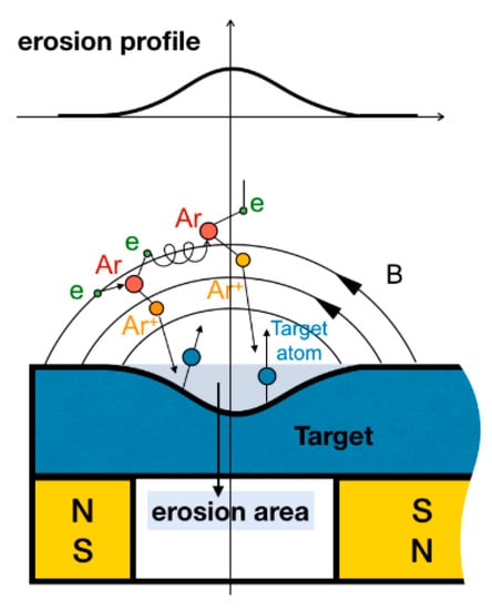
Figure 1.
Etched ring shape.
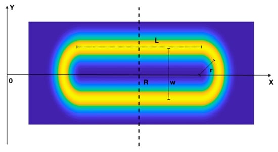
Figure 2.
The rectangular target etching ring orbit.
2.1.3. Sputtering Angle Distribution of Target Particles
At present, the cascade collision model based on momentum transfer theory can better explain the phenomenon of high-speed particle bombardment causing sputtering of target particles [22,23]. When the energy of incident particles is high, nearly all the emissions are normal to the target surface, and practically none are sidewise. On the contrary, the number of particles sputtered near the target surface increases when the energy of incident particles is low. Broadway assumed that the angular distribution curve is an elliptical distribution, as shown in Figure 3 [24]. The expression for this is:
where θ is the angle between the sputtering direction of the particles and the normal direction (Z direction) of the target surface, α = m/n is the ellipticity coefficient, m is the length of the ellipse in the normal direction (Z direction) of the target surface, and n is the minor axis of the ellipse in the tangential direction (X direction) of the target surface. This study quotes this formula, where the major axis of the ellipse and the ellipse coefficient α are set as the parameters to be fitted.
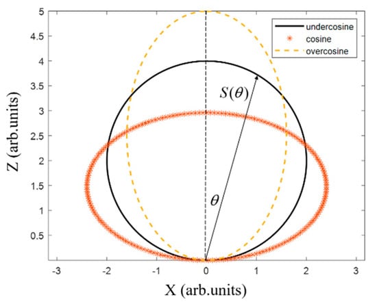
Figure 3.
Angular distribution of particle sputtering on the target surface.
In addition, this study did not discuss the growth process of the film, assuming that the effective deposition coefficient of all particles on the substrate surface is the same. In the case of the barrier of the sleeve to the particles, we simply assumed it was a linear barrier; this means when the substrate and the target are blocked by the sleeve, the contribution of the sputtered particles to the film deposition is not considered.
2.2. Target Particle Sputtering Model
In magnetron sputtering, due to the influence of gas pressure, deposited particles can be roughly divided into fast particles (which do not collide) and slow particles (which collide). Fast particles represent the particles that directly reach the substrate surface without any collisions after sputtering from the target surface, and slow particles represent the particles that reach the substrate surface by diffusive motion, with collisional scattering.
Zhang presents the number of fast particles and number of slow particles deposited per unit area on the substrate by integrating all the positions on the target [25]:
where is the number of sputtered particles per unit area of the target, is the point coordinates on the target, and is the diffusion coefficient .
The total thickness distribution needs to consider both the fast and slow particles. From Equations (4) and (5), we can see that the film thickness distribution is under the influence of geometric parameters: the target–substrate distance, temperature, gas pressure, electromagnetic force, and other factors.
3. Inversion
3.1. Planetary Motion Magnetron Sputtering Coating System
Deposition was carried out using a customized direct current (DC) magnetron sputtering coating system with substrate planetary motion, shown schematically in Figure 4. The diameter of the deposition chamber is 1.4 m. The system was equipped with two rectangular targets (127 mm × 381 mm) with an adjustable height; this means the target–substrate distance was adjustable. In order to avoid the atomic shadow effect, which deteriorates the quality of the deposited film, a rectangular sleeve was used around each target [26,27]. When depositing multilayer films, the two targets were placed symmetrically, and the substrate performed high-speed rotation at a speed of 100 rpm while revolving around the main axis of the system. The rotation of the substrate holder is controlled by an independent rotation switch, while the revolution is controlled by a computer program. During the revolution, the positioning accuracy is better than 1mm. The vacuum system is composed of two sets of mechanical pump and molecular pump; the pumping speed of the molecular pump is 2000 L/s.
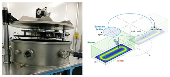
Figure 4.
Planetary motion magnetron sputtering coating system.
Here, the direct coordinate system is used to describe the trajectories of the unit points at different rotational radii of the substrate holder, as shown in Figure 4. Then, the trajectories of the unit points at different rotational radii of the substrate holder can be expressed as:
where R is the rotational radius of the substrate holder, is the revolution angle of the substrate holder, and is the rotational angle of the substrate holder.
The rotational speed of the substrate holder of this experimental device is adjustable by setting the rotational angle change node , and this rotational angle at the rotation angle rate can adjust the rate curve, where the rotational speed between nodes and the rotational angle changes linearly. When calculating the running trajectory, we first segment according to the rotation angle nodes; if there are n nodes, the number of segments is n − 1. Therefore, with the start rotation angle , end rotation angle , start rotation angle rate , and end rotation angle rate of each segment, the rotation rate of each segment may be expressed as:
where ,
Since , the time to turn to is:
where is the start time of this segment and the end time of the previous segment, which can be calculated from the previous segment (for the first segment ).
Since the rotation speed is constant, the rotation angle:
Thus, the trajectories of the unit points at different rotation radii on the substrate holder can be obtained, as shown in Figure 5.
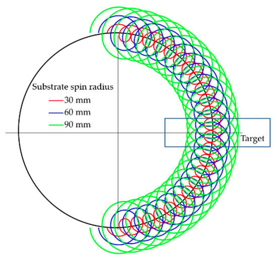
Figure 5.
The trajectory of unit points at different rotation radii on the substrate holder.
3.2. Experimental Inversion
Combining the substrate motion trajectory of 3.1 and the target particle sputtering model of 2.2, the deposition thickness per unit area at different rotation radii on the substrate can be simulated after the following parameters are fitted:
- W target sputtering coefficient ;
- W target etching ring etching width coefficient ;
- W target sputtering angular distribution coefficient ;
- W particle momentum scattering cross-sectional area ;
- W particle diffusion coefficient ;
- Si target sputtering coefficient ;
- Si target etching ring etching width coefficient ;
- Si target sputtering angular distribution coefficient ;
- Si particle momentum scattering cross-sectional area ;
- Si particle diffusion coefficient .
The above parameters are fitted by the following evaluation function:
where and are the model simulation period thickness and calibration sample period thickness at the rotation radius , respectively. is the tolerance of film thickness. In this study, we set equal to 0.2% to make the film thickness close to the ideal value.
In order to reduce the difficulty of fitting, the revolution rate is set to a constant speed when calibrating the multilayer film. At the same time, to ensure the accuracy of the experimental parameter inversion, the two samples, A and B, are coated at different constant revolution speeds. For the substrate, the revolution speeds passing over the W target were 0.200 and 0.211 rpm, and the revolution speeds passing over the Si target were 0.240 and 0.176 rpm, respectively. The deposition conditions are shown in Table 1.

Table 1.
Deposition conditions.
Figure 6 is the normalized curve of the thickness of Sample A and Sample B from the XRR. (The test range is within a radius of 15 to 90 mm, and the film thickness at the radius of 15 mm is the maximum value for normalization. The normalization processing rules in the following text are the same as here.) In the figure, the gradient of Sample B is greater than that of Sample A. When Sample B is coated, the time of coating W is longer than that of Si, while for Sample A it is vice versa. It is inferred that the film thickness gradient of the W layer is greater than that of the Si layer.
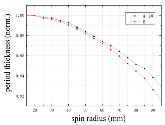
Figure 6.
Comparison of periodic thickness gradient curves of calibration Samples A-1# and B.
The final fitting results are shown in Table 2, and the film thickness distribution calculated by the model is compared with the experimentally obtained film thickness distribution, as shown in Figure 7. The sputtering distribution is the undercosine type because the bombarding particles are argon ions, and their bombardment energy is too small to provide sustained recoil. As a result, the local spike projectile effect is obvious.
Table 2.
Fitting parameters.
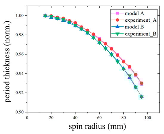
Figure 7.
Comparison of the film thickness distribution calculated by the fitting model and experimental film thickness distribution.
In addition, due to the existence of the sleeve, the particle deposition rate distribution is not a regular ellipse but a rectangular compression. The figure also shows the trajectory of the unit points at different rotation radii. The unit point with a larger rotation radius enters the effective deposition area before the unit point with a smaller rotation radius, but the rate of particle deposition is slower at the larger radius of rotation.
4. Deposition Experiment
4.1. Design Basis of the Speed Curve
After obtaining the particle deposition rate distribution at the moving position of the substrate holder, the substrate holder moving speed curve can be designed to change the film thickness distribution at different rotation radii. At the beginning of designing the variable speed curve, the variable speed node that has the greatest influence on the deposition thickness per unit area at different rotation radii on the substrate holder should be determined.
Figure 8 shows the curve of the deposition thickness (deposition angular rate) per unit revolution angle per unit area at different rotation radii on the substrate holder as a function of the revolution angle, which is faster at small angles because it enters the deposition area first at larger rotation radii. However, when the smaller radius of rotation enters the deposition area, the deposition angle rate increases more rapidly at a small radius than at a large radius, because the smaller the radius of rotation, the closer the trajectory is to the center of the target.
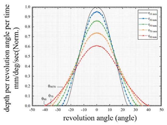
Figure 8.
Film thickness deposition thickness distribution per unit area and unit revolution angle on the substrate holder at different rotation radii.
During the revolution, increasing the revolution speed of the section with an angle of to effectively reduces the difference between the thickness at and the thickness at . For example, in the figure, and are the angles at which effective deposition starts at the rotation radii of 70 and 90 mm, respectively. is the angle at which the angular deposition rate is the same under the radii of rotation of 70 and 90 mm. Therefore, changing the revolution speed from to can efficiently change the relative thickness between the rotation radius of 70 mm and the rotation radius of 90 mm. The thickness at a 90 mm radius of rotation decreases relative to the thickness at a 70 mm radius of rotation as the revolution speed of this section increases.
In order to find this key revolution angle , a third-order polynomial was applied to fit the thickness growth curve:
Then, let the polynomial coefficient of the thickness growth fitting equation at the larger radius be and the polynomial coefficient of the thickness growth fitting equation at the smaller radius be . When the following relation is satisfied, the rate of increase in thickness at the smaller radius begins to exceed that at the larger radius.
Let , then:
With the above cubic polynomial, the key revolution angle for this study could be calculated according to Formula (13). Meanwhile, the revolution speed curve based on the key angle nodes and , which controls the motion of our magnetron sputtering coating system, can be derived as shown in Figure 9.
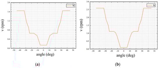
Figure 9.
Revolution speed distribution curve. (a) W target; (b) Si target.
4.2. Results
The film was deposited at a background pressure of 2.6 × 10⁻⁴ Pa and in the presence of Ar, 99.999% purity. The working pressure was controlled at 2 mTorr (1 mTorr = 0.133 Pa). All the depositions were performed while keeping the substrates at room temperature and facing the target at the distance of 120.5 mm, while the W and Si targets were placed diagonally and adjusted to the same height. The sputtering power supply was 50 and 150 W, and the voltage was 327 and 436 V, respectively.
The substrate of the finished product was a parabolic cylinder Si substrate produced by Zeiss. The size of it was 40 mm × 20 mm × 20 mm, and the surface roughness was 0.127–0.155 nm (root mean square roughness).
Since the substrate of the finished product was thick and the shape was parabolic, the surface reflectance could not be measured directly. In this regard, the method of placing a silicon wafer at a symmetrical position in the center of the finished product was applied, as shown in Figure 10, to determine the reflectance and film thickness distribution of the finished wafer by testing the silicon wafer. In order to confirm whether this method was reliable, we placed two calibrated silicon wafers symmetrically and tested the film thickness distribution curve. As shown in Figure 11, the maximum deviation of the overall film thickness was 0.005 nm, so we believe this method is reliable.
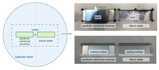
Figure 10.
The placement of the finished product and the calibrated silicon wafer.
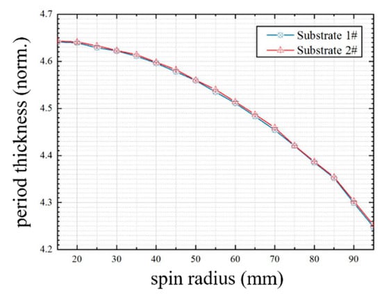
Figure 11.
Comparison chart of the d-spacing of calibration Samples 1# and 2#.
Finally, a laterally graded multilayer film was coated with the revolution speed curve in Figure 9. The thickness distribution test curve is shown in the brown line in Figure 12, with a thickness error of less than 1%. Figure 13 shows the XRR test curve of the finished product with a test interval of 5 mm. The x value is the abscissa value of the parabola where the substrate is located. The larger the x is, the closer the substrate is to the center of rotation on the substrate holder, the better the film quality is, and the higher the reflectivity, owing to fewer obliquely incident particles.
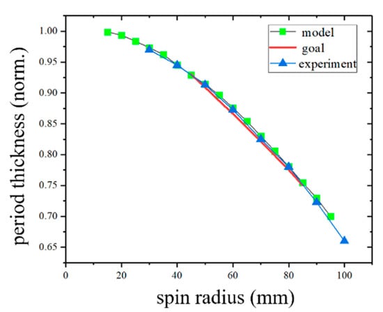
Figure 12.
Film thickness distribution curve (red line: target thickness curve; blue line: simulated thickness curve; brown line: actual coating thickness distribution curve).
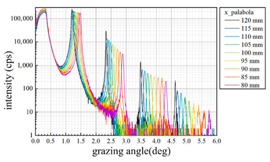
Figure 13.
XRR test curve.
In practical applications, what really affects the working efficiency of the mirror is the shift of the first-order peak position. As shown in Figure 14, the reflected light intensity at the working grazing angle of incidence is always greater than 95% of the peak-to-peak value.
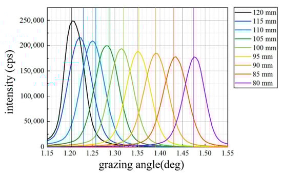
Figure 14.
The first-order peak of the XRR test curve (the straight line is the working grazing incident angle of the position).
5. Conclusions
In this paper, we proposed an effective method for controlling the film thickness distribution. The aim of the study was to find a technology for fabricating laterally graded multilayers required for parabolic collimators, applied in a high-precision diffractometer.
A fast and slow particle transport model was established based on Petrov’s theory, which considered the collisions that occur during the deposition. In order to improve the simulation efficiency and model accuracy, the Gaussian distribution was employed to simulate the etching ring depth, and the sputtering distribution was assumed to be the undercosine type.
A film thickness control model based on the planetary motion magnetron sputtering coating system is presented. The parameters in the model were set as objects to be fitted, and experimental results were introduced to invert the sputtering parameters, which improved the accuracy of the model while reducing the difficulty of model from a practical point of view. We coated two W/Si multilayer film samples, A and B, at different constant revolution speeds, to ensure the accuracy of the experimental parameter inversion.
We also analyzed the film thickness at different radii on the substrate holder under different revolution angles. A third-order polynomial was applied to fit the thickness growth curve to find the key revolution angle, in order to derive the speed curve that controls the motion of our magnetron sputtering coating system and builds the required film thickness distribution.
Finally, we studied the thickness error of the W/Si ML deposited onto the parabolic cylinder Si substrate, and found it was less than 1%. It was shown that the reflected light intensity at the working grazing angle of incidence is always greater than 95% of the peak-to-peak value from the XRR test curve.
In conclusion, it should be noted that these experiments indicate the prospect of using the planetary motion magnetron sputtering coating system and correcting for the fabrication of the laterally graded multilayer.
Author Contributions
Conceptualization, H.H., R.Q. and Z.W.; methodology, R.Q.; software, H.H. and L.J.; validation, R.Q. and Z.W.; formal analysis, H.H.; investigation, H.H., R.Q., L.J. and Z.Z.; resources, R.Q., Z.Z. and Z.W.; data curation, H.H. and Y.Y.; writing original draft preparation, H.H.; writing review and editing, R.Q.; visualization, H.H.; supervision, R.Q., Z.Z. and Z.W.; project administration, R.Q.; funding acquisition, R.Q., Z.Z. and Z.W. All authors have read and agreed to the published version of the manuscript.
Funding
This research was funded by the Research Program of Science and Technology Commission of Shanghai Municipality (20142200500), National Natural Science Foundation of China (12027810, 11805212, 12003016).
Institutional Review Board Statement
Not applicable.
Informed Consent Statement
Not applicable.
Data Availability Statement
The data presented in this study are available on request from the corresponding author.
Conflicts of Interest
All authors have read and approved this version of the article, and due care has been taken to ensure the integrity of the work. Neither the entire paper nor any part of its content has been published or has been accepted elsewhere.
References
- Schuster, M.; Göbel, H. Parallel-beam coupling into channel-cut monochromators using curved graded multilayers. J. Phys. D Appl. Phys. 1995, 28, A270–A275. [Google Scholar] [CrossRef]
- Michaelsen, C.; Ricardo, P.; Anders, D.; Schuster, M.; Schilling, J.; Gobel, H. Improved Graded Mirrors for XRD Applications. Adv. X-ray Anal. 2000, 42, 308–320. [Google Scholar]
- Duplain, G.; Verly, P.G.; Dobrowolski, J.A.; Waldorf, A.; Bussière, S. Graded-reflectance mirrors for beam quality control in laser resonators. Appl. Opt. 1993, 32, 1145–1153. [Google Scholar] [CrossRef] [PubMed]
- McCarthy, N.; Demers, J.-G.; Lavigne, P.; Parent, A. Design and characterization of graded reflectivity mirrors. In Proceedings of the 1986 Quebec Symposium, Quebec, QC, Canada, 3–6 June 1986. [Google Scholar]
- Sassolas, B.; Flaminio, R.; Franc, J.; Michel, C.; Montorio, J.-L.; Morgado, N.; Pinard, L. Masking technique for coating thickness control on large and strongly curved aspherical optics. Appl. Opt. 2009, 48, 3760–3765. [Google Scholar] [CrossRef] [PubMed]
- Morawe, C.; Peffen, J.-C.; Hignette, O.; Ziegler, E. Design and performance of graded multilayers. X-ray Opt. Des. Perform. Appl. 1999, 3773, 90–100. [Google Scholar]
- Nagel, D.J.; Gilfrich, J.V.; Barbee, T.W., Jr. Bragg diffractors with graded-thickness multilayers. Nucl. Instrum. Methods Phys. Res. 1982, 195, 63–65. [Google Scholar] [CrossRef]
- Villa, F.; Martínez, A.; Regalado, L.E. Correction masks for thickness uniformity in large-area thin films. Appl. Opt. 2000, 39, 1602. [Google Scholar] [CrossRef]
- Townsend, J.S. The Conductivity produced in gases by the motion of negatively-charged ions. Nat. Cell Biol. 1900, 62, 340–341. [Google Scholar] [CrossRef]
- Yamamura, Y.; Ishida, M. Monte Carlo simulation of the thermalization of sputtered atoms and reflected atoms in the magnetron sputtering discharge. J. Vac. Sci. Technol. A 1995, 13, 101–112. [Google Scholar] [CrossRef]
- Yagisawa, T.; Makabe, T. Modeling of dc magnetron plasma for sputtering: Transport of sputtered copper atoms. J. Vac. Sci. Technol. A 2006, 24, 908. [Google Scholar] [CrossRef]
- Bauer, E. Phänomenologische Theorie der Kristallabscheidung an Oberflächen. II. Z. Krist. Cryst. Mater. 1958, 110, 395–431. (In German) [Google Scholar] [CrossRef]
- Moskovkin, P.; Lucas, S. Computer simulations of the early-stage growth of Ge clusters at elevated temperatures on patterned Si substrate using the kinetic Monte Carlo method. Thin Solid Films 2013, 536, 313–317. [Google Scholar] [CrossRef]
- Ecker, G.; Emeleus, K.G. Cathode sputtering in glow discharges. Proc. Phys. Soc. Sect. B 1954, 67, 546–552. [Google Scholar] [CrossRef]
- Petrov, I.; Ivanov, I.; Orlinov, V.; Sundgren, J.E. Comparison of magnetron sputter deposition conditions in neon, argon, krypton, and xenon discharges. J. Vac. Sci. Technol. A Vac. Surf. Film 1993, 11, 2733–2741. [Google Scholar] [CrossRef]
- Ekpe, S.D.; Bezuidenhout, L.W.; Dew, S.K. Deposition rate model of magnetron sputtered particles. Thin Solid Films 2005, 474, 330–336. [Google Scholar] [CrossRef]
- Shishkov, M.; Popov, D.; Shishkov, M.; Popov, D. Thickness uniformity of thin films deposited on a flat substrate by sputtering of a target with rotational symmetry. J. Vacuum 1991, 42, 1005–1008. [Google Scholar] [CrossRef]
- Motohiro, T. Applications of Monte Carlo simulation in the analysis of a sputter-deposition process. J. Vac. Sci. Technol. A 1986, 4, 189–195. [Google Scholar] [CrossRef]
- Turner, G.M.; Falconer, I.S.; James, B.W.; McKenzie, D.R. Monte Carlo calculations of the properties of sputtered atoms at a substrate surface in a magnetron discharge. J. Vac. Sci. Technol. A 1992, 10, 455–461. [Google Scholar] [CrossRef]
- Zhu, G.; Sun, J.; Gan, Z. A novel approach to calculate the deposition uniformity of multi-target sputtering system. In Proceedings of the 2018 19th International Conference on Electronic Packaging Technology (ICEPT), Shanghai, China, 8–11 August 2018; IEEE: New York, NY, USA, 2018; pp. 1372–1377. [Google Scholar]
- Vasilev, D.D.; Moiseev, K.M. Influence of the planar cylindrical target erosion zone of magnetron sputtering on the uniformity of a thin-film coating. J. Phys. Conf. Ser. 2015, 584, 12012. [Google Scholar] [CrossRef]
- Biersack, J.P.; Eckstein, W. Sputtering studies with the Monte Carlo Program TRIM.SP. Appl. Phys. A 1984, 34, 73–94. [Google Scholar] [CrossRef]
- Martynenko, Y.V.; Rogov, A.V.; Shul’Ga, V.I. Angular distribution of atoms during the magnetron sputtering of polycrystalline targets. Tech. Phys. 2012, 57, 439–444. [Google Scholar] [CrossRef]
- Broadway, D.M.; Platonov, Y.Y.; Gomez, L.A. Achieving desired thickness gradients on flat and curved substrates. X-ray Opt. Instrum. Mission. II 1999, 3766, 262–275. [Google Scholar]
- Zhang, Y.; Song, Q.; Sun, Z. Research on thin film thickness uniformity for deposition of rectangular planar sputtering target. Phys. Procedia 2012, 32, 903–913. [Google Scholar] [CrossRef]
- Hawkeye, M.M.; Brett, M.J. Glancing angle deposition: Fabrication, properties, and applications of micro- and nanostructured thin films. J. Vac. Sci. Technol. A 2007, 25, 1317. [Google Scholar] [CrossRef]
- Yu, J.; Amar, J.G. Dynamical scaling behavior in two-dimensional ballistic deposition with shadowing. Phys. Rev. E 2002, 66, 21603. [Google Scholar] [CrossRef]


Publisher’s Note: MDPI stays neutral with regard to jurisdictional claims in published maps and institutional affiliations. |
© 2021 by the authors. Licensee MDPI, Basel, Switzerland. This article is an open access article distributed under the terms and conditions of the Creative Commons Attribution (CC BY) license (https://creativecommons.org/licenses/by/4.0/).