Abstract
CH3NH3PbI3 perovskite photovoltaic devices treated with a polysilane layer were fabricated and characterized. Decaphenylcyclopentasilane (DPPS) in chlorobenzene solution was deposited at the surface of the perovskite layer, and the resulting device was annealed at 140–260 °C. The photoconversion efficiencies of the DPPS-treated device remained high even after 255 days in ambient air. Raman scattering spectroscopy and ab initio molecular orbital calculations of DPPS suggested that it increased hole transport efficiency in the treated devices, which was confirmed from the high shunt resistances of the DPPS-treated devices.
1. Introduction
Si-based photovoltaic cells are a widely used energy technology. However, the manufacture of Si-based devices is complex, and the band structure of silicon involves an indirect transition type. Conversely, CH3NH3PbI3 (MAPbI3) has the advantages of a direct bandgap, a high conversion efficiency, and an ability to be solution processed [1,2,3,4,5]. Hence, perovskite compounds are regarded as candidates for new generation photovoltaic materials. However, perovskites are normally unstable in air. The instability of MAPbI3 has been attributed to migration and desorption of CH3NH3 (MA) and reactions with moisture in air [6,7]. Therefore, the stability of perovskite solar cells must be improved to enable their practical application in modules [8,9].
Various doped perovskite crystals have been widely studied with the aim of improving their stability and photovoltaic properties [10,11,12,13]. Although perovskite solar cells doped with CH3(NH2)2 [14,15,16], CH3CH2NH3 [17,18], or C(NH2)3 [19,20] have been developed and studied, these organic molecules may still induce instabilities. Substitutions of CH3NH3 by doping sodium [21], potassium [22,23,24], rubidium, or cesium are expected to be effective for suppressing desorption of CH3NH3 sites in the MAPbI3. Doping Rb+ or Cs+ to the MAPbI3 also reduced defect densities and increased grain sizes [25,26,27,28]. First-principles calculation also indicated that co-doping of alkali metals and copper at the MA and Pb sites, respectively, lowered the distortion and energies of the crystal structures [29,30]. In fact, photovoltaic properties of the co-doped perovskite solar cells were improved and stable, even after one year [31].
Another approach to improving the stability of perovskite solar cells is incorporating polymeric materials into the perovskite devices [32,33,34,35,36,37]. Polymers have been shown to promote device stability in perovskite cells [38]. For example, coating a thin layer of poly(methyl methacrylate) on top of the perovskite layer forms a cross-linked network structure, which protects the cell from moisture and oxygen [38,39,40]. Poly(propylene carbonate) is similarly effective for improving stability, owing to the formation of large crystals of crosslinked perovskite particles with few defects [34].
The stability of the MAPbI3 compounds is affected by moisture and oxygen in the air and is also influenced by the hole transport layer (HTL). A common HTL in perovskite solar cells is 2,2′,7,7′-tetrakis-[N,N-di(p-methoxyphenyl)amine]-9,9′-spirobifluorene (spiro-OMeTAD); however, this HTL is expensive and has poor stability. Alternative low cost and more stable HTLs have been developed [36,37], and other HTL materials, such as polysilanes, have also been utilized with organic photovoltaic devices [41,42].
In contrast to organic polymers, polysilanes have two important features. First, polysilanes are p-type semiconductors, which promote hole transfer. Second, polysilanes are more stable at elevated temperatures above 300 °C than ordinary organic materials. Polysilanes may function as a protective layer when deposited on perovskite compounds. Hence, polysilanes, such as decaphenylcyclopentasilane (DPPS), have been applied as HTLs [43,44] and as additives in the photoactive layer [45] of MAPbI3 perovskite devices. DPPS has been found to promote a uniform perovskite morphology, which increases device power conversion efficiencies. However, chlorobenzene is typically used to dissolve and deposit DPPS by solution processing. Chlorobenzene can also have effects on device performance, which have not been investigated separately from its use as a solvent for DPPS [46,47,48]. Thus, there is a need to separately investigate the effects of DPPS and chlorobenzene in detail.
The purpose of the present work was to investigate the photovoltaic properties and stabilities of perovskite photovoltaic devices treated with a DPPS layer. The cells were treated by high temperature annealing in ambient air. The effects of treating devices with DPPS in chlorobenzene on the photovoltaic properties and microstructures were investigated. When only the DPPS is used as the HTL, the obtained conversion efficiencies are not enough; consequently, the DPPS/spiro-OMeTAD bilayer was applied in the present work. The chlorobenzene-treated devices were also compared to investigate the effect of the chlorobenzene. To increase the conversion efficiency by raising the fabrication temperatures of the devices, the device preparation time was shortened.
2. Experimental and Calculation Procedures
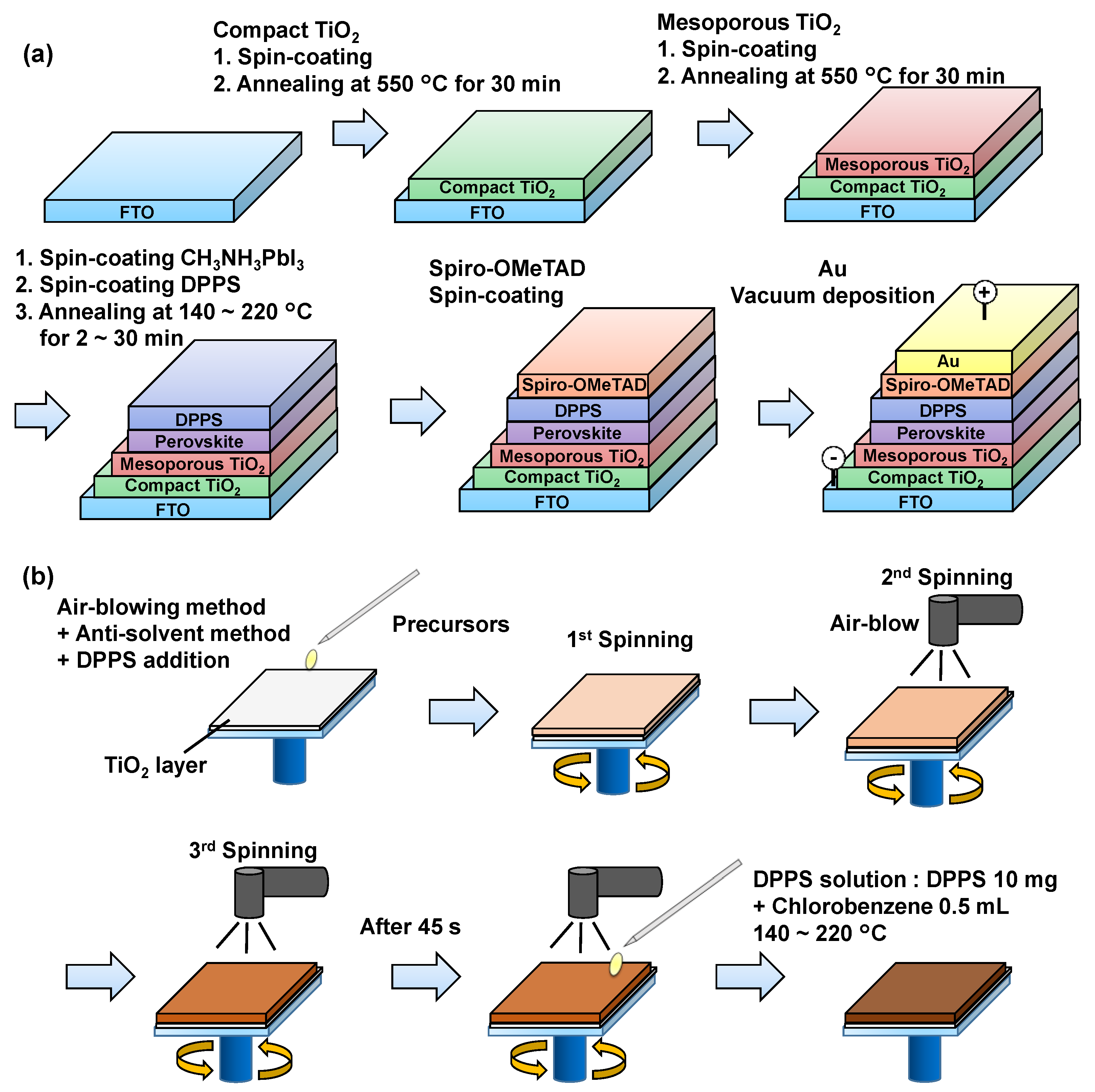
Figure 1a shows the fabrication process of the devices. Detailed conditions for the fabrication process have been described in previous reports [10,48,49,50,51]. All fabrication processes were performed under atmospheric conditions in ambient air, and the temperature and humidity were ~20 °C and ~30%, respectively. A compact TiO2 layer and a mesoporous TiO2 layers were formed on a fluorine-doped tin oxide (FTO) substrate by annealing at 550 °C. To prepare the perovskite compounds, solutions of PbCl2 (Sigma Aldrich, Tokyo, Japan, 111.2 mg) and CH3NH3I (Tokyo Chemical Industry, 190.7 mg) with the desired molar ratio were mixed in N,N-dimethylformamide (Sigma Aldrich, 0.5 mL) at 60 °C for 24 h. These perovskite precursor solutions were normally spin-coated during the first coating. During the second and third spin-coating steps, an air-blowing method was employed [50], as illustrated in Figure 1b. The cells were maintained at 90 °C during the air-blowing. DPPS (Osaka Gas Chemicals, OGSOL SI-30-15, Osaka, Japan, 10 mg) solutions were prepared in chlorobenzene (0.5 mL) and dropped onto the perovskite layer during the last 15 s of the third spin-coating of the perovskite precursor solutions, as shown in Figure 1b. A suitable temperature to initiate the reaction of the starting materials (3CH3NH3I and PbCl2) for forming MAPbI3 and 2CH3NH3Cl (as a gas) is 140 °C [10,50]. The devices with DPPS layers were annealed at temperatures in the range of 140 to 260 °C for 1 to 30 min. Then, a spiro-OMeTAD layer was formed as an HTL by spin-coating, and the spiro-OMeTAD layer was formed below the gold electrodes for all the fabricated devices in the present work. Finally, gold (Au) electrodes were formed by evaporation. All the fabricated cells in the present work were put into dark storage at a temperature of 22 °C and ~30% humidity in ambient air.

Figure 1.
(a) Schematic illustration of the fabrication process of the perovskite photovoltaic devices. (b) Detailed illustration of DPPS insertion process.
Detailed conditions for the characterization of the devices have been described in previous reports [51,52,53]. Microstructural analysis was conducted by an X-ray diffractometer (Bruker, Billerica, MA, USA, D2 PHASER). Raman scattering spectra were measured with a Raman microspectrometer (JASCO, Tokyo, Japan, NRS-5100). The surface morphologies of the perovskite layers were examined using an optical microscope (Nikon, Tokyo, Japan, Eclipse E600). The current density voltage characteristics of the fabricated devices were measured (Keysight, Santa Rosa, CA, USA, B2901A) under a solar simulator (San-ei Electric, Osaka, Japan, XES-301S) with irradiation at 100 mW cm−2. Geometry optimization and energy calculation of the DPPS molecule were performed by the ab initio calculation using the restricted open-shell Hartree–Fock (RHF) method as the approximated wavefunctions with STO-3G* basis set (Gaussian 09) [21,54,55]. The electron density distributions around the lowest unoccupied molecular orbital (LUMO) and the highest occupied molecular orbital (HOMO) were calculated from total self-consistent-field density. The isovalue for the MO on the surface were adjusted to be 0.02 Hartree. The hybrid orbital was widely mapped on the atoms, yielding delocalization. The detailed electron density and Mulliken charge was described in the log file. The electrostatic potential was calculated from the Mulliken population analysis. As the Mulliken population analysis, the charge distribution of atoms was calculated while considering the atomic orbital overlapping and molecular orbital coefficient. The electrostatic potential was displayed on the surface of the isoelectron density and was mapped with electron density from total self-consistent-field density. The density of electrostatic potential was adjusted to be 0.03. Maximum and minimum energy values with the Hartree unit are shown by scale bars. The positive charge was distributed as blue electrostatic potential around the atom. Raman scattering spectra and the vibration modes were calculated by RHF with STO-3G* using frequency mode.
3. Results and Discussion
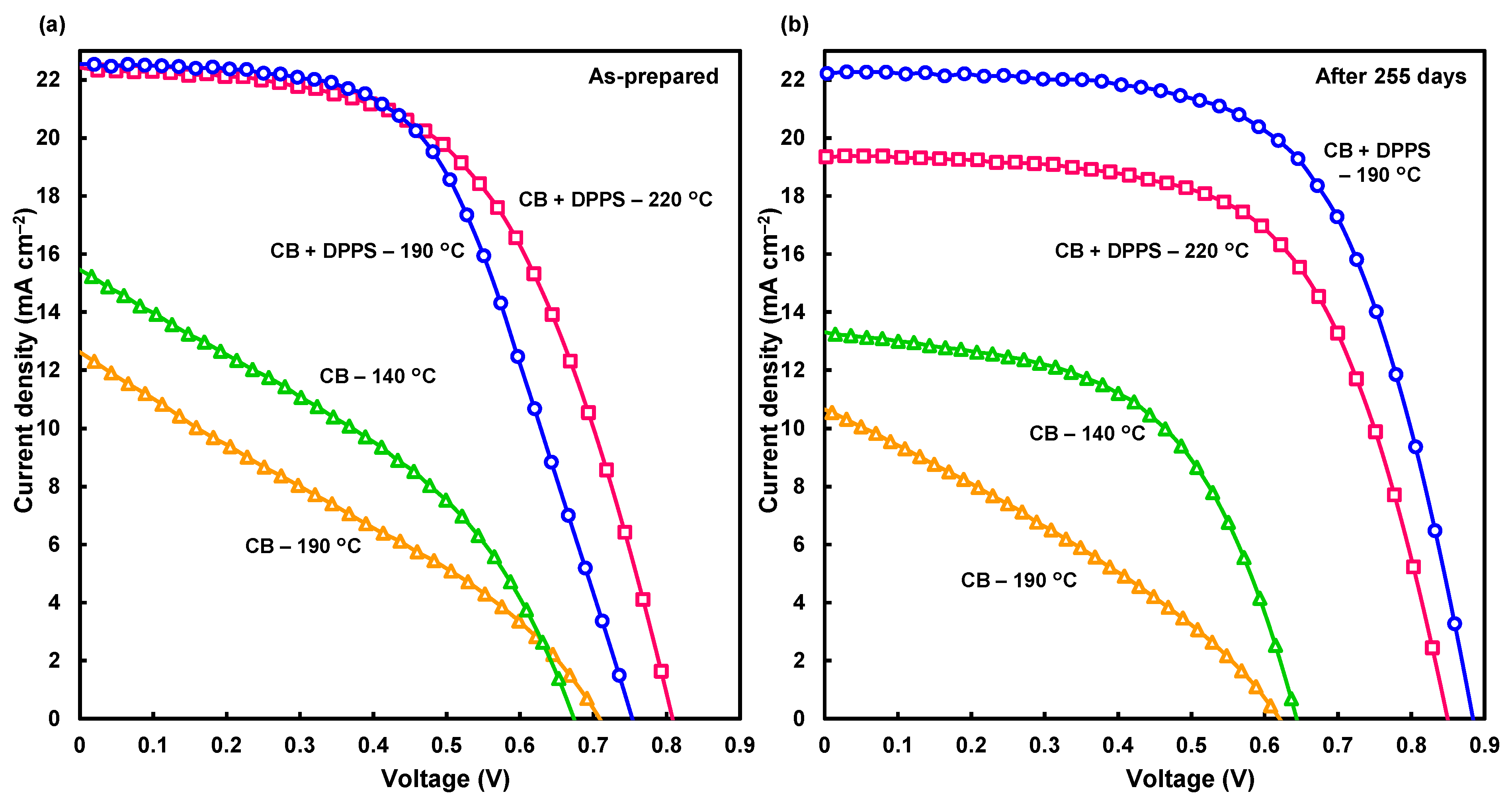
Figure 2a shows current density voltage (J-V) curves of the fabricated solar cells. The performance of the cells is summarized in Table 1. The measured parameters were as follows: VOC: open-circuit voltage, JSC: short-circuit current density, FF: fill factor, η: conversion efficiency, ηave: averaged efficiency of four cells, RS: series resistance, and RSh: shunt resistance. Devices prepared with only chlorobenzene had an η of 3.87% after annealing at 140 °C. To enable a comparison of the chlorobenzene-treated devices with the DPPS-treated devices, a pair of these devices were annealed at 190 °C. The device prepared with DPPS in chlorobenzene had η of 9.40%. The same device fabricated at 220 °C had an initially higher η value of 10.04%. All cell parameters were improved for the devices treated with DPPS in chlorobenzene. The JSC and FF markedly increased compared with those values of the chlorobenzene-treated devices.

Figure 2.
Current density voltage curves of the devices (a) as-prepared and (b) after 255 days in ambient air without encapsulation.

Table 1.
Photovoltaic parameters of perovskite photovoltaic devices. * Prepared from CH3NH3I:PbI2 = 1:1 and without air blowing.
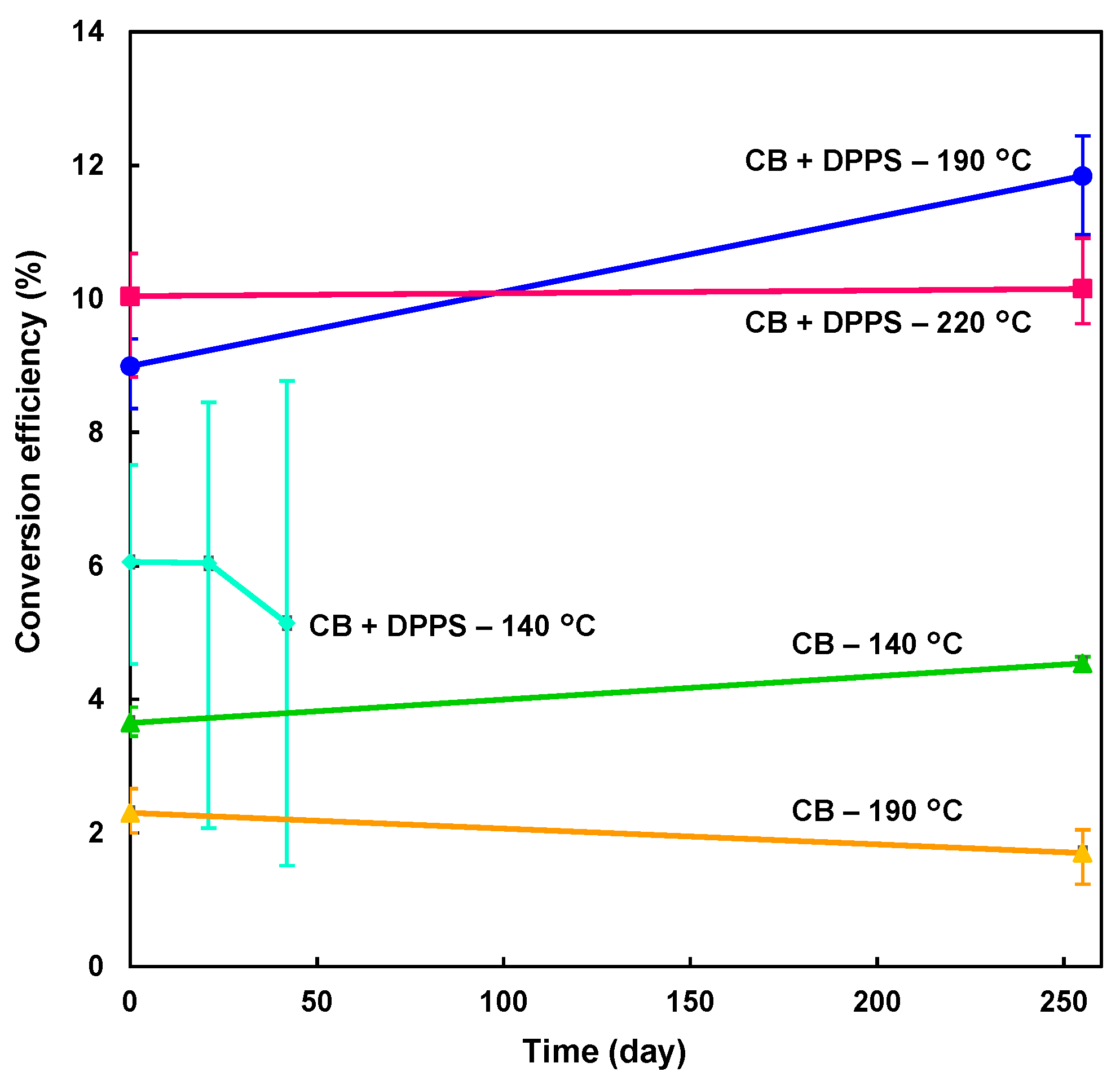
Stabilities of the photovoltaic parameters after preparation in ambient air were measured for the cells over 255 days, and J-V characteristics are shown in Figure 2b. After 255 days, the highest photoconversion efficiency of 12.4% was obtained for the DPPS device prepared at 190 °C (Table 1). The DPPS device prepared at 220 °C had good stability over the extended time, as shown in Figure 3. Whereas the photoconversion efficiency of the chlorobenzene-treated devices prepared at 190 °C decreased over time, η for the devices prepared with DPPS in chlorobenzene at 190 °C increased; hence, DPPS effectively increased the photovoltaic properties when subjected to high temperature annealing. Although the FF values increased for all the devices, VOC decreased for the chlorobenzene-treated device after 255 days. Conversely, VOC for the DPPS-treated devices increased. The hysteresis index (HI) is also calculated and listed in Table 1. The HI values were estimated from the next equation [56]: HI = (JRH − JFH)/JRH, where JRH is the current density at the half open-circuit voltage for the reverse scan, and JFH is the current density at the half open-circuit voltage for the forward scan. When there is no hysteresis, the HI is equal to 0. Although the HI values of CB devices were lower than those of CB + DPPS devices for the as-prepared cells, HI values of CB + DPPS and CB devices decreased and increased after 255 days, respectively. The parameters of the DPPS devices either remained stable or increased over time, which is attributed to the reduced influence of moisture, oxygen, and spiro-OMeTAD in the DPPS protected perovskite layers. Shunt resistances were high for the DPPS-added devices, which is likely because of the effects of DPPS on hole transport and electron blocking [45,48].

Figure 3.
Stabilities of the present devices.
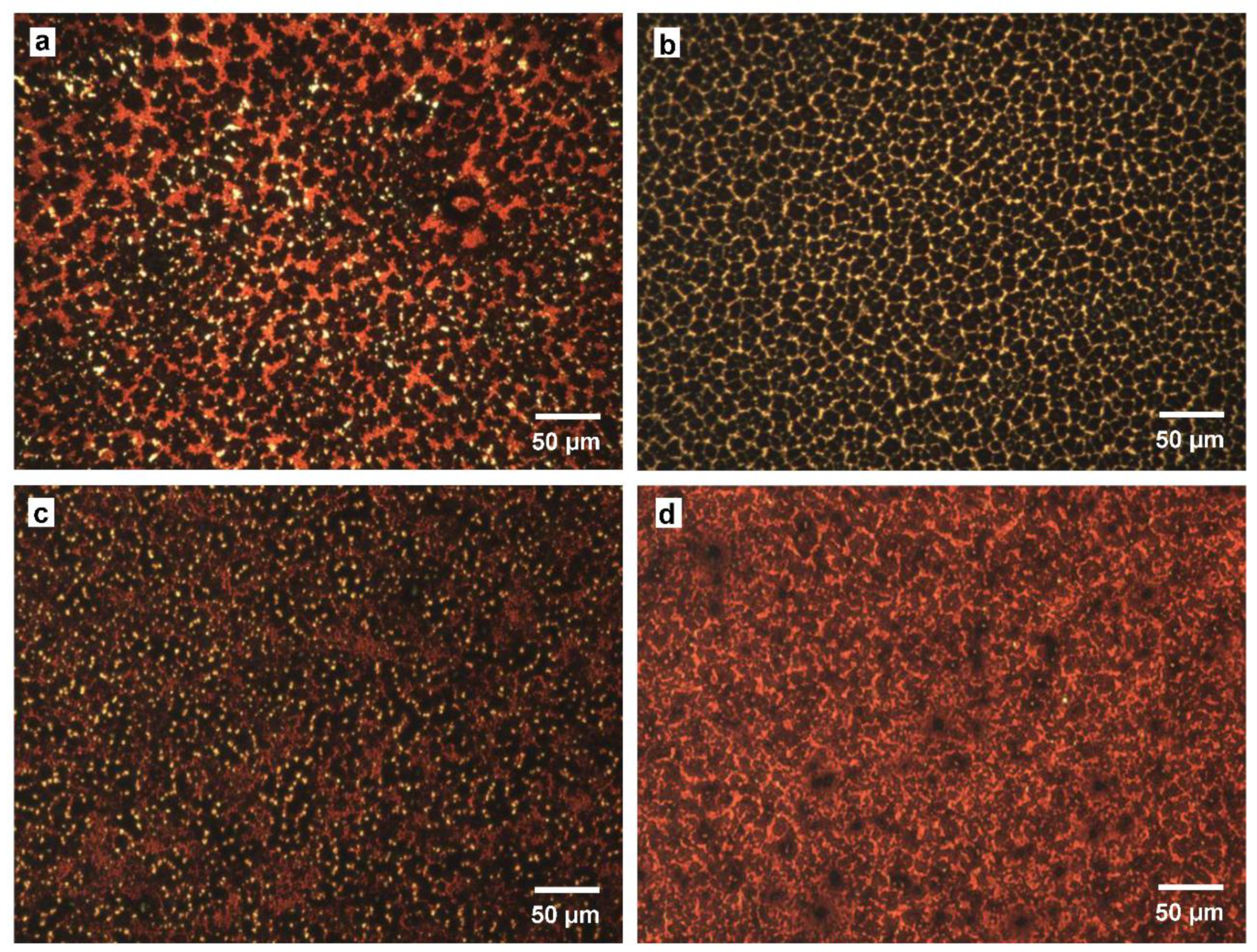
Optical microscope images of the perovskites in the present devices measured after 255 days are shown in Figure 4. The perovskite grains were dispersed and divided by space for the chlorobenzene-treated devices, as observed in Figure 4a,b. On the other hand, the morphologies of the perovskite changed drastically by adding DPPS, and the perovskite grains seems to form smoother surface. Hence, the DPPS-treated devices had fewer grain boundaries and a greater surface coverage of grains. This morphology should suppress carrier recombination and reduce carrier losses. These effects were confirmed by the low RS and high RSh values for the DPPS-treated devices.

Figure 4.
Optical microscope images of cells prepared with chlorobenzene and annealed at (a) 140 °C and (b) 190 °C; and cells prepared with DPPS in chlorobenzene annealed at (c) 190 °C and (d) 220 °C.
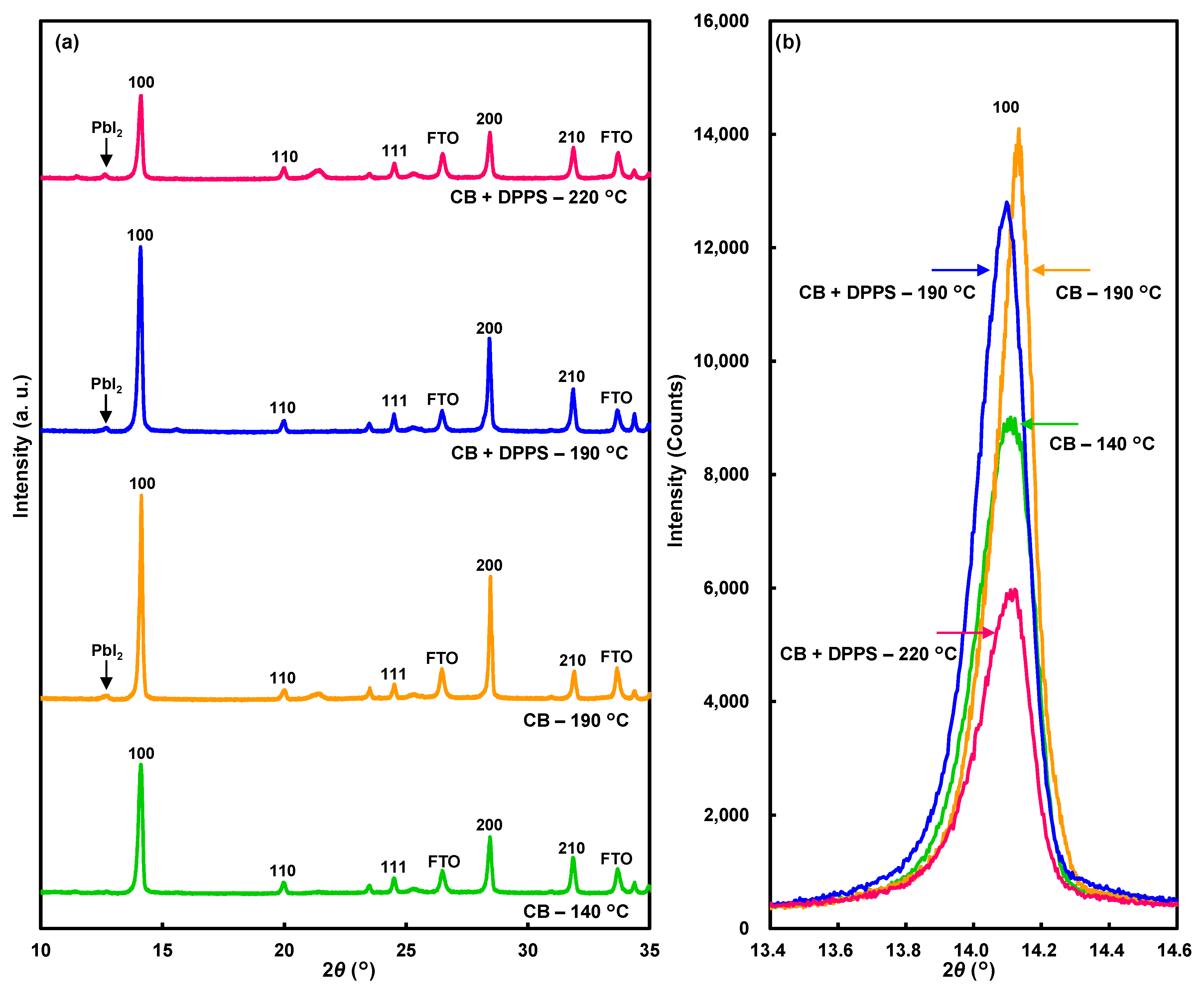
Figure 5a shows X-ray diffraction (XRD) results of the devices after 255 days. The diffraction patterns were indexed to a cubic perovskite structure [10,49]. The (100) diffraction peaks were higher for both the devices treated with chlorobenzene and DPPS in chlorobenzene prepared at 190 °C, as observed in the enlarged XRD patterns in Figure 5b.

Figure 5.
(a) X-ray diffraction patterns of the devices. (b) Enlarged patterns of 100 reflections.
The lattice constant of the perovskite compound decreased slightly at 220 °C (Table 2), which indicated desorption of MA. The lattice constant was smallest for the chlorobenzene device prepared at 190 °C, indicating that the MA desorption was associated with a decrease in conversion efficiency. The device treated with DPPS in chlorobenzene at 190 °C had the largest lattice constant, indicating that the MA desorption was suppressed, contributing to the high efficiency.

Table 2.
Crystallographic data of perovskite films.
The crystal orientation of the perovskite grains was estimated from the ratios of the 100 intensity (I100) to the 210 intensity (I210) in the XRD patterns, as summarized in Table 2. When the crystal planes in the perovskite crystallites were randomly aligned, the intensity ratio of I100/I210 was 2.08 [10]. For the device prepared with chlorobenzene at 190 °C, I100/I210 was 7.5, which indicates that the (100) planes were comparatively well aligned with the FTO substrate. For the devices treated with DPPS in chlorobenzene, I100/I210 decreased to 4.4 after annealing at 190 °C to 2.7 for devices annealed at 220 °C. Hence, the DPPS treatment of the perovskite promoted more randomly aligned structures. Small PbI2 peaks were observed for both devices treated with chlorobenzene and DPPS in chlorobenzene after annealing at 190 °C. Further formation of PbI2 was suppressed during annealing at 220 °C, which indicates that the DPPS protected the MAPbI3 crystals against decomposition to PbI2.
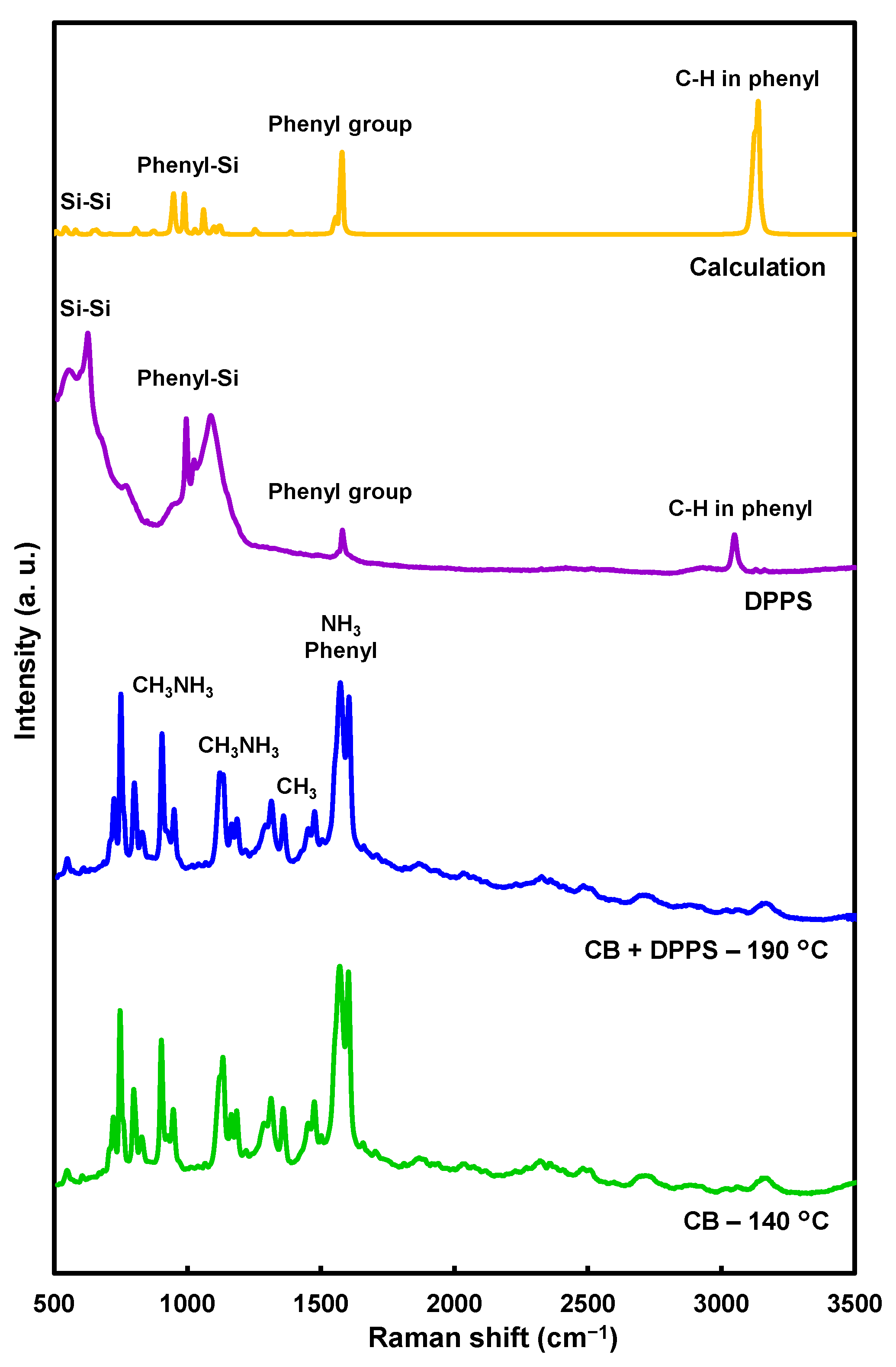
Raman spectroscopy measurements of DPPS and the present as-prepared photovoltaic devices are shown in Figure 6, together with calculated data for the DPPS. The Raman scattering peaks at ~600, ~1100, ~1540, and ~3040 cm−1 are respectively assigned to Si-Si, phenyl-Si, phenyl group, and phenyl C-H groups of the DPPS. Several peaks were assigned to MA, CH3, and NH3 for the devices treated with chlorobenzene and DPPS in chlorobenzene. These peaks derive from internal vibrations of MA relating to its local symmetry in the crystal symmetry [57,58]. Because the amount of DPPS was quite small, no clear differences were apparent in the Raman spectra of the devices treated with chlorobenzene and DPPS in chlorobenzene.

Figure 6.
Raman spectra of DPPS and devices.
In this study, the DPPS was dissolved in chlorobenzene, which is often used as an antisolvent to promote grain growth and form smooth surface structures on perovskite films, resulting increased current densities [59,60,61]. Although temperatures around ~100 °C are commonly used to fabricate perovskite devices, high temperatures above ~180 °C are required to improve the efficiencies of DPPS-treated cells. Thus, DPPS affects the morphology and photoelectronic properties by a different mechanism from that of chlorobenzene. The DPPS layer suppresses MA desorption and DPPS is also a p-type semiconductor, which has hole transporting properties that inhibit hole and electron recombination.
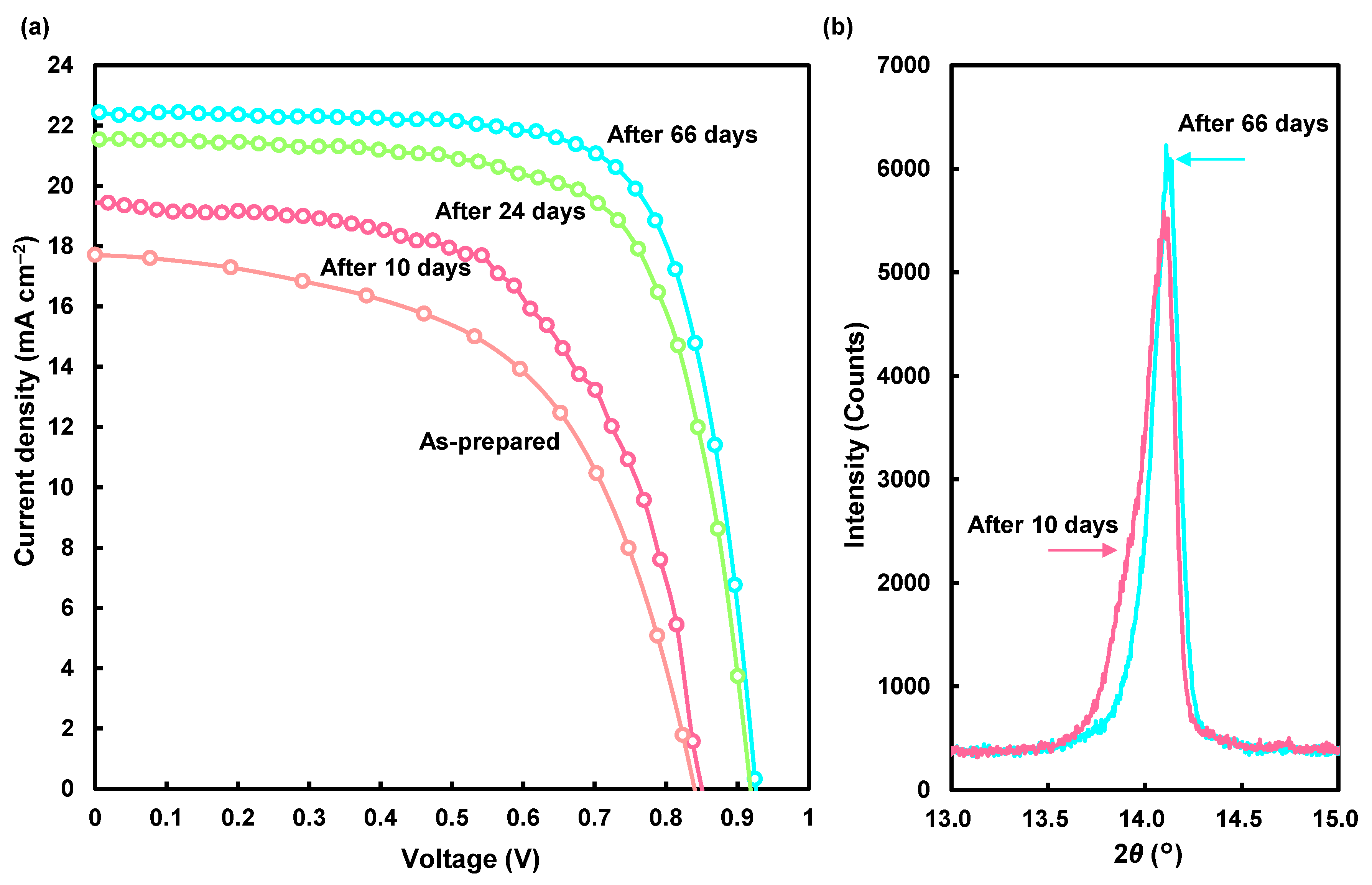
The J-V characteristics of the champion DPPS-treated device with the highest conversion efficiency in the present work are also shown in Figure 7, and the measured photovoltaic parameters are listed in Table 3. The device was annealed at 190 °C for 5 min. Although the conversion efficiency of this as-prepared device was lower than that prepared at 190 °C for 30 min, its efficiency increased to ~15% after 66 days. Changes of the (100) XRD reflections for the champion device in the present work are shown in Figure 7b, and the crystallographic data are summarized in Table 4. The perovskite crystallites were randomly aligned after 10 days, and the intensity ratio of I100/I210 increased from 1.9 to 2.6 after 66 days, which indicates that the (100) planes were comparatively well aligned. In addition, the crystallite size increased from 486 to 617 Å after 66 days. This indicates that the increase of the conversion efficiencies would be caused by the crystal growth of the perovskite compounds during room temperature aging. This crystallization mechanism even after the annealing at the high temperature of 190 °C would be explained by the DPPS treatment, which might slow the diffusion of ions and crystal growth during annealing. Then, the non-crystalized phase that remained might contribute to the crystal growth during the aging.

Figure 7.
(a) Changes of the J-V curves for the champion device in the present work. (b) X-ray diffraction patterns of 100 reflections.

Table 3.
Photovoltaic parameters of champion device, treated with DPPS in chlorobenzene and annealed at 190 °C for 5 min.

Table 4.
Changes of crystallographic data of perovskite films.
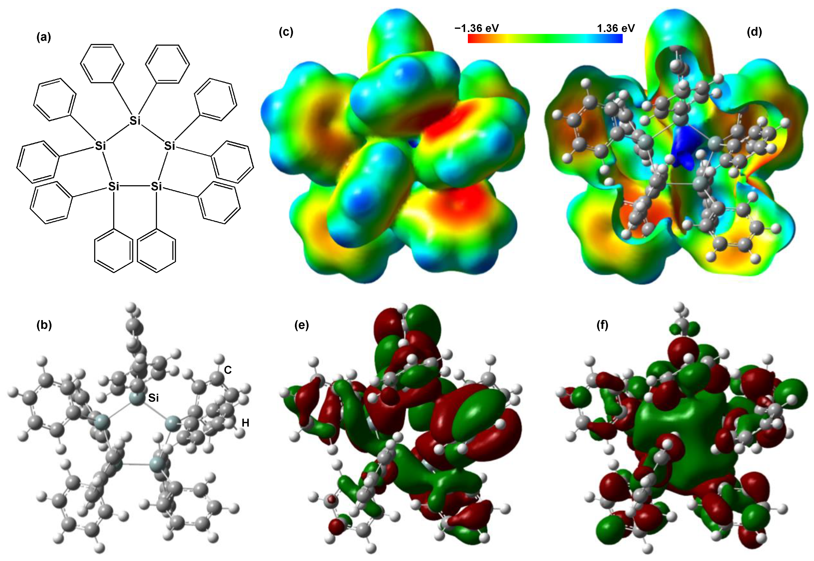
Schematic and optimized structural models of DPPS are shown in Figure 8a,b, respectively. Pentagonal Si bonding is present in both models. Figure 8c,d shows an electrostatic potential map of DPPS and its cutaway view, respectively, as calculated by ab initio methods based on the HF. The electrostatic potential was positive (blue) around the cyclopentasilane and proton, as shown in Figure 8c,d. Calculated electronic structures of the DPPS at the HOMO and the LUMO energy levels are shown in Figure 8e,f, respectively. The phases of electron densities in the Si-3p and C-2p orbitals were inverted, as indicated by the green and red coloration. The electronic charge of the HOMO was broadly distributed over the phenyl rings and Si-Si chains, which contributed to the carrier transport and electronic properties. The length of the main Si-Si chain also affects the localization of σ electrons, which determines the LUMO level.

Figure 8.
(a) Schematic and (b) optimized models of DPPS. (c) Electrostatic potential, (d) cutaway view of (c), (e) HOMO, and (f) LUMO.
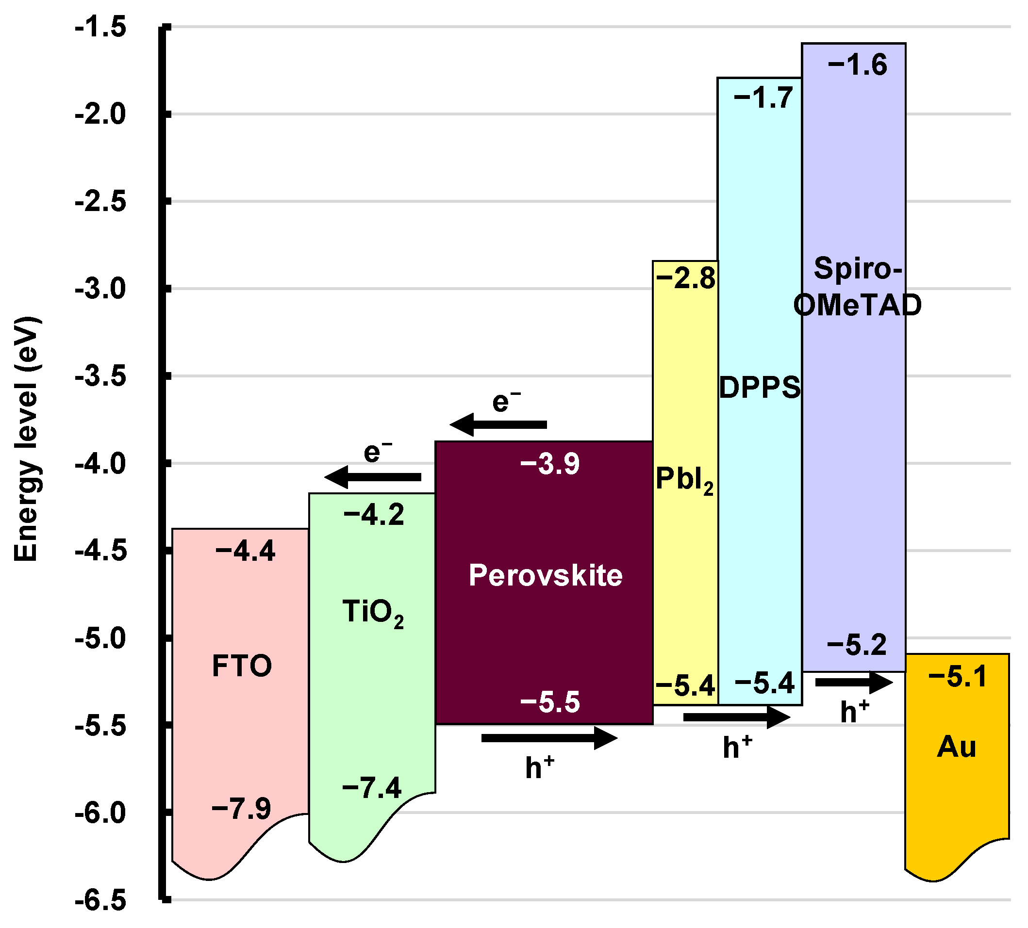
An energy level diagram of the present DPPS-treated perovskite cells is shown in Figure 9. The energy levels of the valence band maximum, conduction band minimum, HOMO, and LUMO are indicated in the diagram [62,63]. When the device was irradiated from the FTO glass side, carriers (holes and electrons) separate at the interfaces. Holes separated in the perovskite layer are carried through the PbI2, DPPS, and spiro-OMeTAD to the gold electrode. Conversely, electrons are transported through titanium dioxide to the FTO. By inserting a DPPS layer between the photoactive layer and the HTL, holes are effectively transported from the valence band maximum of the MAPbI3 to the Fermi level of Au. High shunt resistances were obtained for the DPPS-treated devices, which are attributed to the hole transporting and formation of smoother surface morphology by DPPS. Efficient carrier transport is likely caused by the specific arrangement of the phenyl group around the cyclopentasilane in the DPPS [41].

Figure 9.
Energy level diagram of the present cell.
A small PbI2 layer might be formed by MA desorption at the perovskite/DPPS interface at high temperatures. If this thin PbI2 layer forms at the perovskite/DPPS interface during or after annealing, PbI2 may act as a p-type semiconductor and an HTL [64,65]. Activation energies of ion migration of MA+, I− and Pb2+ in the MAPbI3 were reported to be 0.84, 0.58, and 2.31 eV, respectively [66]. Since the activation energy of Pb2+ migration is higher than those of other ions, the formed PbI2 layer may remain around the surface of the perovskite. The increased efficiency of the DPPS-treated devices might also be related to crystallization of amorphous grains. During the spin-coating of DPPS, a composite layer of DPPS and amorphous pre-perovskite compounds forms, which provides a solid interface for room temperature aging. Because DPPS can also function as a hole transport material [41], holes are efficiently transported at the interface, to improve the Rsh and VOC. Since all the processes in the present work were performed in the ambient air, further improvement of photovoltaic properties is expected by controlling the environmental conditions.
4. Conclusions
In summary, the effects of a DPPS treatment on perovskite solar cells were investigated. The DPPS layer was inserted at the perovskite/spiro-OMeTAD interface. Conversion efficiencies improved by inserting the DPPS layer during spin-coating of MAPbI3 and annealing above 190 °C. A cell fabricated at 220 °C had the highest photoconversion efficiency among the as-fabricated cells, and the conversion efficiencies of all devices remained stable over more than 8 months in air. In addition, a device fabricated at 190 °C had the highest efficiency following room temperature aging. The DPPS layer acts as both a protective layer for the perovskite and as an HTL. Although a small amount of PbI2 was detected by XRD, the PbI2 layer likely also functioned as an HTL. The perovskite grains grew more densely, and their surface coverage increased compared with that resulting from the ordinary chlorobenzene anti-solvent method. The DPPS treatment promoted fewer lattice defects and grain boundaries, which suppressed the leakage current and increased the JSC. The effectiveness of the DPPS on hole transport was also confirmed by ab initio molecular orbital calculations. These findings indicate that high temperature annealing of devices treated with DPPS in chlorobenzene is an effective and easy method for improving the photoconversion efficiencies and stability of MAPbI3 solar cells.
Author Contributions
Conceptualization, T.O. and M.T.; methodology, T.O., M.T., A.S., K.K., Y.A. and S.Y.; formal analysis, T.O., M.T, A.S., K.K., Y.A. and S.Y.; investigation, M.T., Y.A., K.K., A.S. and S.Y.; resources, M.O., S.M., S.F. and T.T.; data curation, T.O., M.T., K.K. and Y.A.; writing—original draft preparation, T.O.; writing—review and editing, M.T., A.S., K.K., Y.A., S.Y., M.O., S.M., S.F. and T.T.; project administration, T.O.; funding acquisition, T.O. All authors have read and agreed to the published version of the manuscript.
Funding
This research was partly funded by the Super Cluster Program of the Japan Science and Technology Agency (JST) and by a Grant-in-Aid for Scientific Research (C) 21K04809.
Institutional Review Board Statement
Not Applicable.
Informed Consent Statement
Not Applicable.
Data Availability Statement
Data is contained within the article.
Conflicts of Interest
The authors declare no conflict of interest.
References
- Gedamu, D.; Asuo, I.M.; Benetti, D.; Basti, M.; Ka, I.; Cloutier, S.G.; Rosei, F.; Nechache, R. Solvent-antisolvent ambient processed large grain size perovskite thin films for high-performance solar cells. Sci. Rep. 2018, 8, 12885. [Google Scholar] [CrossRef] [PubMed]
- Mingyu, J.; Choi, I.W.; Go, E.M.; Cho, Y.; Kim, M.; Byongkyu, L.; Seonghun, J.; Yimhyun, J.; Choi, H.W.; Lee, J.; et al. Stable perovskite solar cells with efficiency exceeding 24.8% and 0.3-V voltage loss. Science 2020, 369, 1615–1620. [Google Scholar] [CrossRef]
- Miyasaka, T.; Kulkarni, A.; Kim, G.M.; Öz, S.; Jena, A.K. Perovskite solar cells: Can we go organic-free, lead-free, and dopant-free? Adv. Energy Mater. 2020, 10, 1902500. [Google Scholar] [CrossRef]
- Tong, J.; Song, Z.; Kim, D.M.; Chen, X.; Chen, C.; Palmstrom, A.F.; Ndione, P.F.; Reese, M.O.; Dunfield, S.P.; Reid, O.G.; et al. Carrier lifetimes of >1 μs in Sn-Pb perovskites enable efficient all-perovskite tandem solar cells. Science 2019, 364, 475–479. [Google Scholar] [CrossRef] [PubMed]
- Wang, F.; Yang, M.; Yang, S.; Qu, X.; Yang, L.; Fan, L.; Yang, J.; Rosei, F. Iodine-assisted antisolvent engineering for stable perovskite solar cells with efficiency >21.3%. Nano Energy 2020, 67, 104224. [Google Scholar] [CrossRef]
- Dunfield, S.P.; Bliss, L.; Zhang, F.; Luther, J.M.; Zhu, K.; van Hest, M.F.A.M.; Reese, M.O.; Berry, J.J. From defects to degradation: A mechanistic understanding of degradation in perovskite solar cell devices and modules. Adv. Energy Mater. 2020, 10, 1904054. [Google Scholar] [CrossRef]
- Lee, J.W.; Kim, S.G.; Yang, J.M.; Yang, Y.; Park, N.G. Verification and mitigation of ion migration in perovskite solar cells. APL Mater. 2019, 7, 041111. [Google Scholar] [CrossRef]
- Zhang, X.; Yin, J.; Nie, Z.; Zhang, Q.; Sui, N.; Chen, B.; Zhang, Y.; Qu, K.; Zhao, J.; Zhou, H. Lead-free and amorphous organic–inorganic hybrid materials for photovoltaic applications: Mesoscopic CH3NH3MnI3/TiO2 heterojunction. RSC Adv. 2017, 7, 37419–37425. [Google Scholar] [CrossRef]
- Dong, H.; Wu, Z.; Xi, J.; Xu, X.; Zuo, L.; Lei, T.; Zhao, X.; Zhang, L.; Hou, X. Pseudohalide-induced recrystallization engineering for CH3NH3PbI3 film and its application in highly efficient inverted planar heterojunction perovskite solar cells. Adv. Funct. Mater. 2017, 28, 1704836. [Google Scholar] [CrossRef]
- Oku, T. Crystal structures of perovskite halide compounds used for solar cells. Rev. Adv. Mater. Sci. 2020, 59, 264–305. [Google Scholar] [CrossRef]
- Travis, W.; Glover, E.N.K.; Bronstein, H.; Scanlon, D.O.; Palgrave, R.G. On the application of the tolerance factor to inorganic and hybrid halide perovskites: A revised system. Chem. Sci. 2016, 7, 4548–4556. [Google Scholar] [CrossRef]
- Hoefler, S.F.; Trimmel, G.; Rath, T. Progress on lead-free metal halide perovskites for photovoltaic applications: A review. Monatsh. Chem. 2017, 148, 795–826. [Google Scholar] [CrossRef] [PubMed]
- Tanaka, H.; Oku, T.; Ueoka, N. Structural stabilities of organic–inorganic perovskite crystals. Jpn. J. Appl. Phys. 2018, 57, 08RE12. [Google Scholar] [CrossRef]
- Zhou, Y.; Yang, M.; Pang, S.; Zhu, K.; Padture, N.P. Exceptional morphology-preserving evolution of formamidinium lead triiodide perovskite thin films via organic-cation displacement. J. Am. Chem. Soc. 2016, 138, 5535–5538. [Google Scholar] [CrossRef]
- Hu, M.; Liu, L.; Mei, A.; Yang, Y.; Liu, T.; Han, H. Efficient hole conductor-free, fully printable mesoscopic perovskite solar cells with a broad light harvester NH2CH=NH2PbI3. J. Mater. Chem. A 2014, 2, 17115–17121. [Google Scholar] [CrossRef]
- Suzuki, A.; Kato, M.; Ueoka, N.; Oku, T. Additive effect of formamidinium chloride in methylammonium lead halide compound-based perovskite solar cells. J. Electron. Mater. 2019, 48, 3900–3907. [Google Scholar] [CrossRef]
- Wang, Y.; Zhang, T.; Li, G.; Xu, F.; Li, Y.; Yang, Y.; Zhao, Y. A mixed-cation lead iodide MA1-xEAxPbI3 absorber for perovskite solar cells. J. Energy Chem. 2018, 27, 215–218. [Google Scholar] [CrossRef]
- Nishi, K.; Oku, T.; Kishimoto, T.; Ueoka, N.; Suzuki, A. Photovoltaic characteristics of CH3NH3PbI3 perovskite solar cells added with ethylammonium bromide and formamidinium iodide. Coatings 2020, 10, 410. [Google Scholar] [CrossRef]
- Jodlowski, A.D.; Roldán-Carmona, C.; Grancini, G.; Salado, M.; Ralaiarisoa, M.; Ahmad, S.; Koch, N.; Camacho, L.; Miguel, G.; Nazeeruddin, M. Large guanidinium cation mixed with methylammonium in lead iodide perovskites for 19% efficient solar cells. Nat. Energy 2017, 2, 972–979. [Google Scholar] [CrossRef]
- Kishimoto, T.; Suzuki, A.; Ueoka, N.; Oku, T. Effects of guanidinium addition to CH3NH3PbI3-xClx perovskite photovoltaic devices. J. Ceram. Soc. Jpn. 2019, 127, 491–497. [Google Scholar] [CrossRef]
- Suzuki, A.; Miyamoto, Y.; Oku, T. Electronic structures, spectroscopic properties, and thermodynamic characterization of sodium or potassium-incorporated CH3NH3PbI3 by first principles calculation. J. Mater. Sci. 2020, 55, 9728–9738. [Google Scholar] [CrossRef]
- Zheng, F.; Chen, W.; Bu, T.; Ghiggino, K.P.; Huang, F.; Cheng, Y.; Tapping, P.; Kee, T.W.; Jia, B.; Wen, X. Triggering the passivation effect of potassium doping in mixed-cation mixed-halide perovskite by light illumination. Adv. Energy Mater. 2019, 9, 1901016. [Google Scholar] [CrossRef]
- Machiba, H.; Oku, T.; Kishimoto, T.; Ueoka, N.; Suzuki, A. Fabrication and evaluation of K-doped MA0.8FA0.1K0.1PbI3(Cl) perovskite solar cells. Chem. Phys. Lett. 2019, 730, 117–123. [Google Scholar] [CrossRef]
- Kandori, S.; Oku, T.; Nishi, K.; Kishimoto, T.; Ueoka, N.; Suzuki, A. Fabrication and characterization of potassium- and formamidinium-added perovskite solar cells. J. Ceram. Soc. Jpn. 2020, 128, 805–811. [Google Scholar] [CrossRef]
- Bush, K.A.; Frohna, K.; Prasanna, R.; Beal, R.E.; Leijtens, T.; Swifter, S.A.; McGehee, M.D. Compositional engineering for efficient wide band gap perovskites with improved stability to photoinduced phase segregation. ACS Energy Lett. 2018, 3, 428–435. [Google Scholar] [CrossRef]
- Liu, C.; Kong, W.; Li, W.; Chen, H.; Li, D.; Wang, W.; Xu, B.; Cheng, C.; Jen, A.K.Y. Enhanced stability and photovoltage for inverted perovskite solar cells via precursor engineering. J. Mater. Chem. A 2019, 7, 15880–15886. [Google Scholar] [CrossRef]
- Zhang, M.; Yun, J.S.; Ma, Q.; Zheng, J.; Lau, C.F.J.; Deng, X.; Kim, J.; Kim, D.; Seidel, J.; Green, M.A.; et al. High-efficiency rubidium-incorporated perovskite solar cells by gas quenching. ACS Energy Lett. 2017, 2, 438–444. [Google Scholar] [CrossRef]
- Turren-Cruz, S.H.; Saliba, M.; Mayer, M.T.; Juárez-Santiesteban, H.; Mathew, X.; Nienhaus, L.; Tress, W.; Erodici, M.P.; Sher, M.J.; Bawendi, M.G.; et al. Enhanced charge carrier mobility and lifetime suppress hysteresis and improve efficiency in planar perovskite solar cells. Energy Environ. Sci. 2018, 11, 78–86. [Google Scholar] [CrossRef]
- Ueoka, N.; Oku, T.; Suzuki, A. Additive effects of alkali metals on Cu-modified CH3NH3PbI3-δClδ photovoltaic devices. RSC Adv. 2019, 9, 24231–24240. [Google Scholar] [CrossRef]
- Ueoka, N.; Oku, T. Effects of co-addition of sodium chloride and copper(II) bromide to mixed-cation mixed-halide perovskite photovoltaic devices. ACS Appl. Energy Mater. 2020, 3, 7272–7283. [Google Scholar] [CrossRef]
- Ueoka, N.; Oku, T.; Suzuki, A. Effects of doping with Na, K, Rb, and formamidinium cations on (CH3NH3)0.99Rb0.01Pb0.99Cu0.01I3-x(Cl, Br)x perovskite photovoltaic cells. AIP Adv. 2020, 10, 125023. [Google Scholar] [CrossRef]
- Chen, Z.; Dong, Q.; Liu, Y.; Bao, C.; Fang, Y.; Lin, Y.; Tang, S.; Wang, Q.; Xiao, X.; Bai, Y.; et al. Thin single crystal perovskite solar cells to harvest below-bandgap light absorption. Nat. Commun. 2017, 8, 1–7. [Google Scholar] [CrossRef] [PubMed]
- Wang, F.; Shimazaki, A.; Yang, F.; Kanahashi, K.; Matsuki, K.; Miyauchi, Y.; Takenobu, T.; Wakamiya, A.; Murata, Y.; Matsuda, K. Highly efficient and stable perovskite solar cells by interfacial engineering using solution-processed polymer layer. J. Phys. Chem. C 2017, 121, 1562–1568. [Google Scholar] [CrossRef]
- Han, T.H.; Lee, J.W.; Choi, C.; Tan, S.; Lee, C.; Zhao, Y.; Dai, Z.; Marco, N.D.; Lee, S.J.; Bae, S.H.; et al. Perovskite-polymer composite cross-linker approach for highly-stable and efficient perovskite solar cells. Nat. Commun. 2019, 10, 520. [Google Scholar] [CrossRef] [PubMed]
- Kim, G.W.; Choi, H.; Kim, M.; Lee, J.; Son, S.Y.; Park, T. Hole transport materials in conventional structural (n–i–p) perovskite solar cells: From past to the future. Adv. Energy Mater. 2020, 10, 1903403. [Google Scholar] [CrossRef]
- Calió, L.; Kazim, S.; Grätzel, M.; Ahmad, S. Hole-transport materials for perovskite solar cells. Angew. Chem. Int. Ed. 2016, 55, 14522–14545. [Google Scholar] [CrossRef]
- Singh, R.; Singh, P.K.; Bhattacharya, B.; Rhee, H.-W. Review of current progress in inorganic hole-transport materials for perovskite solar cells. Appl. Mater. Today 2019, 14, 175–200. [Google Scholar] [CrossRef]
- Bi, D.; Yi, C.; Luo, J.; Decoppet, J.D.; Zhang, F.; Zakeeruddin, S.M.; Li, X.; Hagfeldt, A.; Gratzel, M. Polymer-templated nucleation and crystal growth of perovskite films for solar cells with efficiency greater than 21%. Nat. Energy 2016, 1, 16142. [Google Scholar] [CrossRef]
- Taguchi, M.; Suzuki, A.; Tanaka, H.; Oku, T. Fabrication and characterization of perovskite solar cells added with MnCl2, YCl3 or poly(methyl methacrylate). AIP Conf. Proc. 2018, 1929, 020012. [Google Scholar] [CrossRef]
- Taguchi, M.; Suzuki, A.; Ueoka, N.; Oku, T. Effects of poly(methyl methacrylate) addition to perovskite photovoltaic devices. AIP Conf. Proc. 2019, 2067, 020018. [Google Scholar] [CrossRef]
- Oku, T.; Nakagawa, J.; Iwase, M.; Kawashima, A.; Yoshida, K.; Suzuki, A.; Akiyama, T.; Tokumitsu, K.; Yamada, M.; Nakamura, M. Microstructures and photovoltaic properties of polysilane-based solar cells. Jpn. J. Appl. Phys. 2013, 52, 04CR07. [Google Scholar] [CrossRef]
- Nakagawa, J.; Oku, T.; Suzuki, A.; Akiyama, T.; Yamada, M.; Fukunishi, S.; Kohno, K. Effects of PBr3 addition to polysilane thin films on structures and photovoltaic properties. Green Sustain. Chem. 2017, 7, 20–34. [Google Scholar] [CrossRef]
- Shirahata, Y.; Yamamoto, Y.; Suzuki, A.; Oku, T.; Fukunishi, S.; Kohno, K. Effects of polysilane-doped spiro-OMeTAD hole transport layers on photovoltaic properties. Phys. Status Solidi A 2017, 214, 1600591. [Google Scholar] [CrossRef]
- Shirahata, Y.A.; Oku, T.; Fukunishi, S.; Kohno, K. Fabrication of perovskite-type photovoltaic devices with polysilane hole transport layers. Mater. Sci. Appl. 2017, 8, 209–222. [Google Scholar] [CrossRef]
- Oku, T.; Nomura, J.; Suzuki, A.; Tanaka, H.; Fukunishi, S.; Minami, S.; Tsukada, S. Fabrication and characterization of CH3NH3PbI3 perovskite solar cells added with polysilanes. Int. J. Photoenergy 2018, 8654963. [Google Scholar] [CrossRef]
- Taguchi, M.; Suzuki, A.; Oku, T.; Fukunishi, S.; Minami, S.; Okita, M. Effects of decaphenylcyclopentasilane addition on photovoltaic properties of perovskite solar cells. Coatings 2018, 8, 461. [Google Scholar] [CrossRef]
- Taguchi, M.; Suzuki, A.; Oku, T.; Ueoka, N.; Minami, S.; Okita, M. Effects of annealing temperature on decaphenylcyclopentasilane-inserted CH3NH3PbI3 perovskite solar cells. Chem. Phys. Lett. 2019, 737, 136822. [Google Scholar] [CrossRef]
- Oku, T.; Kandori, S.; Taguchi, M.; Suzuki, A.; Okita, M.; Minami, S.; Fukunishi, S.; Tachikawa, T. Polysilane-inserted methylammonium lead iodide perovskite solar cells doped with formamidinium and potassium. Energies 2020, 13, 4776. [Google Scholar] [CrossRef]
- Oku, T.; Zushi, M.; Imanishi, Y.; Suzuki, A.; Suzuki, K. Microstructures and photovoltaic properties of perovskite-type CH3NH3PbI3 compounds. Appl. Phys. Express 2014, 7, 121601. [Google Scholar] [CrossRef]
- Oku, T.; Ohishi, Y.; Ueoka, N. Highly (100)-oriented CH3NH3PbI3(Cl) perovskite solar cells prepared with NH4Cl using an air blow method. RSC Adv. 2018, 8, 10389–10395. [Google Scholar] [CrossRef]
- Oku, T.; Ohishi, Y.; Suzuki, A.; Miyazawa, Y. Effects of NH4Cl addition to perovskite CH3NH3PbI3 photovoltaic devices. J. Ceram. Soc. Jpn. 2017, 125, 303–307. [Google Scholar] [CrossRef]
- Ueoka, N.; Oku, T.; Tanaka, H.; Suzuki, A.; Sakamoto, H.; Yamada, M.; Minami, S.; Miyauchi, S.; Tsukada, S. Effects of PbI2 addition and TiO2 electron transport layers for perovskite solar cells. Jpn. J. Appl. Phys. 2018, 57, 08RE05. [Google Scholar] [CrossRef]
- Oku, T.; Ohishi, Y. Effects of annealing on CH3NH3PbI3(Cl) perovskite photovoltaic devices. J. Ceram. Soc. Jpn. 2018, 126, 56–60. [Google Scholar] [CrossRef]
- Suzuki, A.; Oku, T. Effects of transition metals incorporated into perovskite crystals on the electronic structures and magnetic properties by first-principles calculation. Heliyon 2018, 4, e00755. [Google Scholar] [CrossRef]
- Suzuki, A.; Oku, T. Effects of mixed-valence states of Eu-doped FAPbI3 perovskite crystals studied by first-principles calculation. Mater. Adv. 2021, 2. in press. [Google Scholar] [CrossRef]
- Chen, H.-W.; Sakai, N.; Ikegami, M.; Miyasaka, T. Emergence of hysteresis and transient ferroelectric response in organo-lead halide perovskite solar cells. J. Phys. Chem. Lett. 2014, 6, 164–169. [Google Scholar] [CrossRef]
- Pérez-Osorio, M.A.; Lin, Q.; Phillips, R.T.; Milot, R.L.; Herz, L.M.; Johnston, M.B.; Giustino, F. Raman spectrum of the organic–inorganic halide perovskite CH3NH3PbI3 from first principles and high-resolution low-temperature Raman measurements. J. Phys. Chem. C 2018, 122, 21703–21717. [Google Scholar] [CrossRef]
- Brivio, F.; Frost, J.M.; Skelton, J.M.; Jackson, A.J.; Weber, O.J.; Weller, M.T.; Goñi, A.R.; Leguy, A.M.A.; Barnes, P.R.F.; Walsh, A. Lattice dynamics and vibrational spectra of the orthorhombic, tetragonal, and cubic phases of methylammonium lead iodide. Phys. Rev. B 2015, 92, 144308. [Google Scholar] [CrossRef]
- Jeon, N.J.; Noh, J.H.; Kim, Y.C.; Yang, W.S.; Ryu, S.; Seok, S. Solvent engineering for high-performance inorganic–organic hybrid perovskite solar cells. Nat. Mater. 2014, 13, 897–903. [Google Scholar] [CrossRef] [PubMed]
- Xiao, M.; Huang, F.; Huang, W.; Dkhissi, Y.; Zhu, Y.; Etheridge, J.; Weale, A.G.; Bach, U.; Cheng, Y.B.; Spiccia, L. A fast deposition-crystallization procedure for highly efficient lead iodide perovskite thin-film solar cells. Angew. Chem. Int. Ed. 2014, 53, 9898–9903. [Google Scholar] [CrossRef] [PubMed]
- Tavakoli, M.M.; Yadav, P.; Prochowicz, D.; Sponseller, M.; Osherov, A.; Bulovic, V.; Kong, J. Controllable perovskite crystallization via antisolvent technique using chloride additives for highly efficient planar perovskite solar cells. Adv. Energy Mater. 2019, 9, 1803587. [Google Scholar] [CrossRef]
- Noh, J.H.; Im, S.H.; Heo, J.H.; Mandal, T.N.; Seok, S.I. Chemical management for colorful, efficient, and stable inorganic–organic hybrid nanostructured solar cells. Nano Lett. 2013, 13, 1764–1769. [Google Scholar] [CrossRef]
- Haga, Y.; Harada, Y. Photovoltaic characteristics of phthalocyanine-polysilane composite films. Jpn. J. Appl. Phys. 2001, 40, 855–861. [Google Scholar] [CrossRef]
- Chen, Q.; Zhou, H.; Song, T.B.; Luo, S.; Hong, Z.; Duan, H.S.; Dou, L.; Liu, Y.; Yang, Y. Controllable self-induced passivation of hybrid lead iodide perovskites toward high performance solar cells. Nano Lett. 2014, 14, 4158–4163. [Google Scholar] [CrossRef] [PubMed]
- Ueoka, N.; Oku, T. Stability characterization of PbI2-added CH3NH3PbI3−xClx photovoltaic devices. ACS Appl. Mater. Interfaces 2018, 10, 44443–44451. [Google Scholar] [CrossRef] [PubMed]
- Eames, C.; Frost, J.M.; Barnes, P.R.F.; O’Regan, B.C.; Walsh, A.; Islam, M.S. Ionic transport in hybrid lead iodide perovskite solar cells. Nat. Commun. 2015, 6, 7497. [Google Scholar] [CrossRef] [PubMed]
Publisher’s Note: MDPI stays neutral with regard to jurisdictional claims in published maps and institutional affiliations. |
© 2021 by the authors. Licensee MDPI, Basel, Switzerland. This article is an open access article distributed under the terms and conditions of the Creative Commons Attribution (CC BY) license (https://creativecommons.org/licenses/by/4.0/).

