1. Introduction
Tantalum nitride (TaN
x) coating is attracting increasing attention due to its high hardness, high corrosion resistance, good tribological properties and chemical inertness; and thus, TaN
x coating has been extensively used in the microeletronic industry as diffusion barriers and thin coating resistors [
1,
2,
3]. Usually, TaN
x coatings are deposited by the physical vapor deposition (PVD) (e.g., reactive magnetron sputtering using a Ta target in a N
2/Ar gas mixture [
4]). However, TaN
x coating synthesized by reactive magnetron sputtering shows a variety of the stoichiometry, such as Ta
2N, TaN, Ta
4N
5, and Ta
5N
6, due to its defective structure, i.e., high vacancy concentrations of atomic lattice sites can be present during the synthesis of TaN
x thin coatings [
5,
6,
7,
8]. It is believed that the chemical composition and crystalline structure of the as-deposited TaN
x coatings strongly depend on the deposition technique and the process parameters, such as sputtering power source (e.g., DC [
4], RF [
9], pulsed power [
10]), N
2/Ar ratio [
11], bias voltage [
12], substrate temperature [
13], pressure [
14] in the growth chamber, etc.
RF magnetron sputtering is capable of depositing a more uniform and stable coating free of dislocations and crystallographic imperfections compared with other conventional magnetron sputtering (e.g., DC magnetron sputtering). Tan et al. [
15] carried out a study to compare the chromium nitride coatings deposited by DC and RF magnetron sputtering, and found that the CrN
x coatings showed optimized microstructure (dense structure) and properties (high hardness) due to the improved plasma density and ion bombardment from the RF condition. In fact, numerous researchers have used RF sputtering to prepare TaN
x coatings and also studied the influences of the process parameters such as N
2 partial pressure [
16] and input power [
9] on the growth, structure and properties of the coatings. Bias voltage applied on the substrate holder has been considered as an effective approach to enhance the delivered energy to the growing coatings and the mobility of adatoms and hence promotes densification of structure as well as grain-refining of the coatings [
17]. Meymian et al. [
18] studied the influence of the bias voltage (0~−250 V) on the Cu
3N films deposited by RF magnetron sputtering and found that the grain sizes decreased and the surface morphology of the films became smoother as the bias voltage increased. It is clear that optimizing the bias voltage is one of the best ways to improve the structure and properties of the coatings. Kuo et al. [
12] prepared TaN
x coatings by RF magnetron sputtering with bias voltage ranging from 0 to −200 V and found that the bias voltage has a significant effect on the coating composite (TaN, Ta
2N and β-Ta phases appeared and/or coexisted in the films at specific biases). However, the influences of the bias voltage on the mechanical and tribological properties of the TaN
x coatings were absent.
In this paper, TaNx coatings were deposited by RF magnetron sputtering with different bias voltages applied on the substrates. The influences of the bias voltage on the structure, hardness and elastic modulus, adhesion strength, tribological performance of the coatings were studied systematically. The relationships between the deposition process, structure and properties were discussed carefully. It is worth noting that, besides N2 partial pressure, the bias voltage is one of the effective ways to control the phase structure of the TaNx coatings.
2. Materials and Methods
Series of TaNx coatings were deposited on the silicon wafers and well-polished stainless steel (SU304) sheets by the RF magnetron sputtering with using Ar/N2 mixture to sputter Ta target (purity 99.99%, 60 mm in diameter). The substrate is about 10 cm distant from the target. An ultrasonic bath with acetone and ethanol was used to clean the substrates for 10 min. Then the substrates were dried in N2. The chamber was evacuated to 5 × 10⁻³ Pa and simultaneously heated up to 300 °C. This temperature was further maintained until the end of the coating process. DC glow discharge with a bias voltage of −700 V was used to etch the substrates for 10 min. Subsequently, in order to improve the adhesion of the TaNx coatings, 200 nm Ta interlayer was deposited on the substrates by sputtering the Ta target. Before the coating process, pre-sputtering was performed for 5 min to remove any impurities on the target surface. During the coating process, a gas mixture of Ar and N2 (Ar/N2 = 30/30 sccm) was introduced into the chamber as the sputtering gas. The deposition pressure was kept around 0.5 Pa. The rotation speed of the substrate holder was set at 1.0 rpm. RF power (RFK30ZC-SW5, Kyosan, Yokohama, Japan) was used for the sputtering process. The RF power was set at approximately 200 W. The bias voltage ranged from 0 V (floating) to −300 V. The deposition duration was 2 h.
Scanning electron microscopy (SEM, Hitachi S-4800, Tokyo, Japan) was used to observe the surface topography and cross-sectional images of the TaNx coatings. X-ray diffraction (XRD, D8-Discovery Bruker, Karlsruhe, Germany) with 1.54 Å Cu Kα radiation was employed to examine the crystal structure of the TaNx coatings under an asymmetric model. X-ray photoelectron spectroscopy (XPS, Thermo ESCALAB 250Xi, Waltham, MA, USA) with Al (mono) Kα (hv = 1486.6 eV) was applied to characterize the coating chemical composition and chemical bonds with a step size of 1 eV. The high-resolution XPS spectra with a step size of 0.05 eV were also taken for the coatings. Before the XPS measurement, the sample surface was etched by an Ar+ ion beam with an energy of 2 kV for 300 s (the etch depth was about 10 nm) to remove contaminants and oxide on the coating surface. The contents of the coating elements were calculated from the relative area ratios of the peaks in the XPS spectra divided by the corresponding atomic sensitivity factors.
Nano-indentation (CSM, NHT2, Anton Paar, Graz, Austrian) with the Berkovich diamond indenter was used to measure the hardness and elastic modulus of the TaNx coatings using a constant load of 5 mN. In order to eliminate the effect of the soft substrate, the maximum indentation depths were chosen around 1/10th of the coating thicknesses. Each sample was tested 15 times to reduce errors. The coating adhesion strength was tested by a Nano Scratch Tester (CSM, Revetest scratch tester, Anton Paar, Graz, Austrian) using Rockwell C diamond styli with radius 200 um with a normal load ranging from 1 to 100 N. The scratch length and scratch speed were 3 mm and 6 mm/min, respectively. An optical microscope (Leica DM2500 M, Wetzlar, German) was used to observe the scratch after the scratch test. A ball-on-plate tribometer (CSM, THT, Anton Paar) was employed to measure the tribological performances of the TaNx coatings with a rotational speed of 200 r/min under a load of 1 N (the initial Hertzian contact pressure was about 0.2 GPa) at room temperature and relative humidity of 50% ± 5% conditions. SU304 balls (6 mm in diameter) were used as the counterpart material. The total wear durations were 60 cycles and 300 cycles for one sample. After the tests, the wear tracks were measured by using a laser scanning confocal microscope (OLS4100, Olympus, Tokyo, Japan). In addition, energy dispersive X-ray spectroscopy (EDX) mapping was also carried out on the wear track to detect the composition of the tribological layer.
3. Results and Discussion
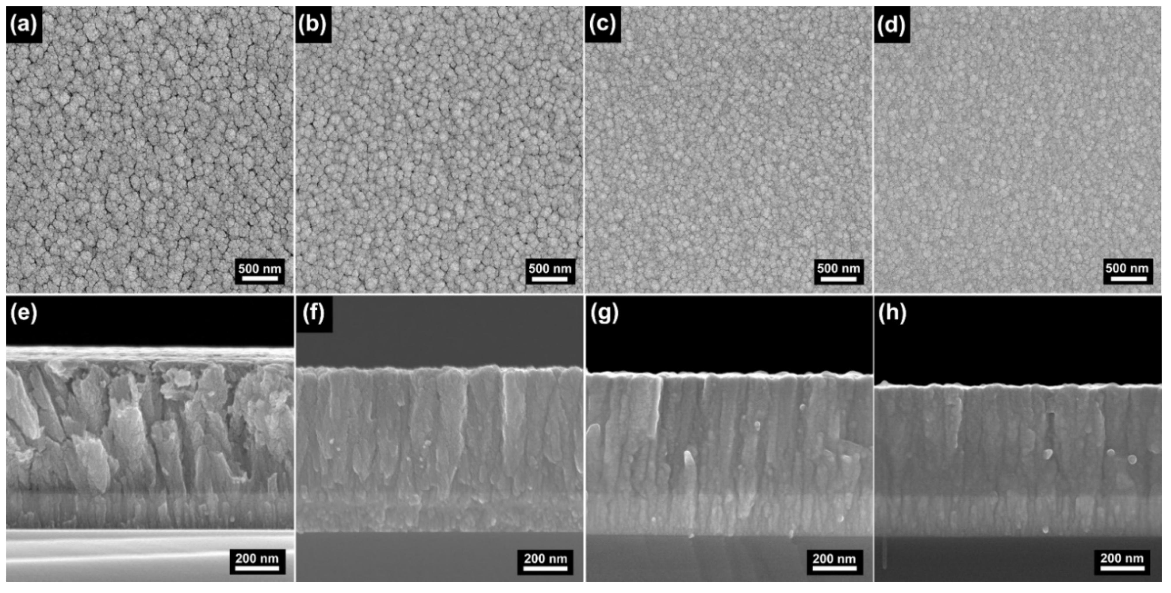
Figure 1 shows the surface topographies and cross-sectional morphologies of the TaN
x coatings deposited with different bias voltages. The TaN
x coating deposited at 0 V (
Figure 1a,e) shows a coarse columnar structure and granular surface. It can be seen that there are numerous crevices between the columnar and granular structures. As the bias voltage increases, it should be noted that the columnar and granular size show a remarkable decrease, implying that the size of the columnar crystal decreases. Additionally, the crevices are degenerating and the coating structure is getting compact with increasing bias voltage. These results are consistent with the results reported in the literature [
19]. An increasing bias voltage would improve the mobility of adatoms and refine the columnar grains. Simultaneously, the increase of the bias voltage would enhance the bombardment effect which contributes to remove defects and facilitates structure densification. However, the increase of the bias voltage also would increase the so-called “self-sputtering” effect that causes the etching of the coating surface [
12]. As a result, the thickness of the coatings was decreasing with increasing bias voltage, as shown in the cross-sectional images of
Figure 1e–g.
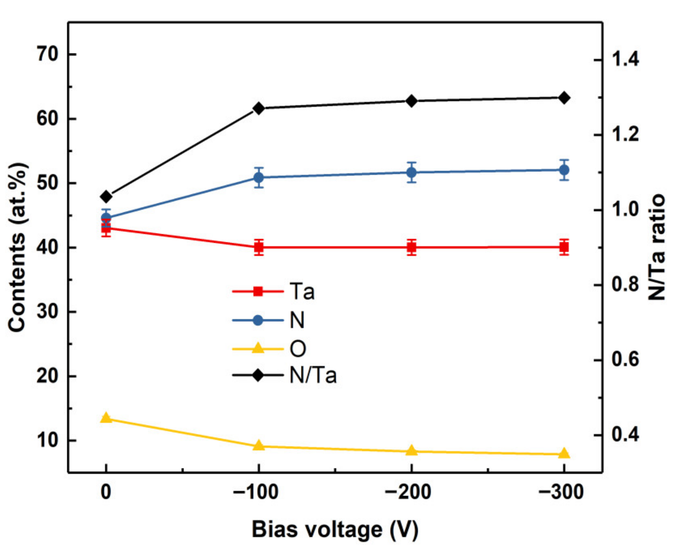
The evolution of the Ta, N and O contents and the N/Ta ratio in the TaN
x coatings are presented in
Figure 2 as a function of the bias voltage. It can be seen that the Ta and N contents show a slow growth as the bias voltage increases. The N/Ta ratio also increases slowly with the bias voltage. It is supposed that an increasing bias would enhance the nitrogen doping in the coatings. Oxygen was detected in the coatings and the content decreases with the bias voltage. There are two main reasons for the existence of oxygen in the coatings. Firstly, the residual oxygen in the chamber due to the relatively high base pressure would cause the introduction of oxygen in the coatings. Secondly, the existence of oxygen might be mainly attributed to the exposure of the samples before the XPS test. As shown in the SEM images of
Figure 1, the coating deposited at 0 V has a loose and porous structure. The oxygen can be absorbed on these defects. Accordingly, the oxygen content is very high in the XPS test even after etching by Ar
+ beam for 300 s. As the bias voltage increases, the coating structure became compact and dense, reducing the phenomenon of oxygen adsorption.
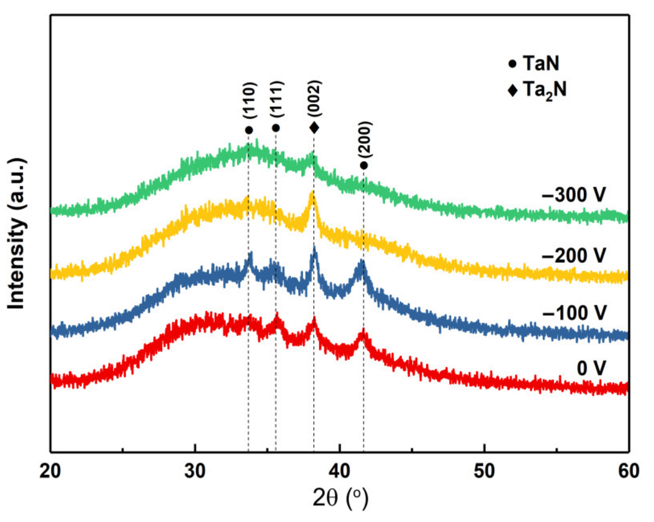
Figure 3 shows the XRD patterns of the TaN
x coatings deposited with different bias voltages. The XRD pattern of the coating deposited at 0 V presents diffraction peaks at 2θ angles of 33.7°, 35.5°, 41.6°, which can be identified as the TaN (110), (111) and (200). It is worth noting that there is a peak around 38.2°, which can be identified as the (002) plane of Ta
2N. This indicates that the coating is mainly consisting of TaN and Ta
2N crystals. As the bias voltage increases to −100 V, the diffraction peaks of the coatings become stronger and shaper, implying that the crystallinity of the coatings is enhanced. It is believed that the bias voltage can enhance the delivered energy to the growing coatings and the mobility of adatoms and hence improves the crystallinity of the coatings. As the bias voltage increases to −200 V, the diffraction peaks of TaN disappear and the crystal structure transfers to the Ta
2N. When the bias voltage increases further (−300 V), the Ta
2N peak tends to be wider and degenerated, implying that the grain size of the coatings gradually reduces and evolved into an amorphous structure. This result is consistent with the SEM images. It is also worth noting that the Ta
2N phase is more stable than the TaN phase under different bias voltages. Actually, the Ta
2N phase is stable in a relatively wide nitrogen concentration range and the process window is therefore wide than that of the TaN phase in the phase diagram [
20]. Accordingly, it is believed that, besides the N
2 partial pressure, the bias voltage is also a significant factor that influences the phase composition of the TaN
x coatings.
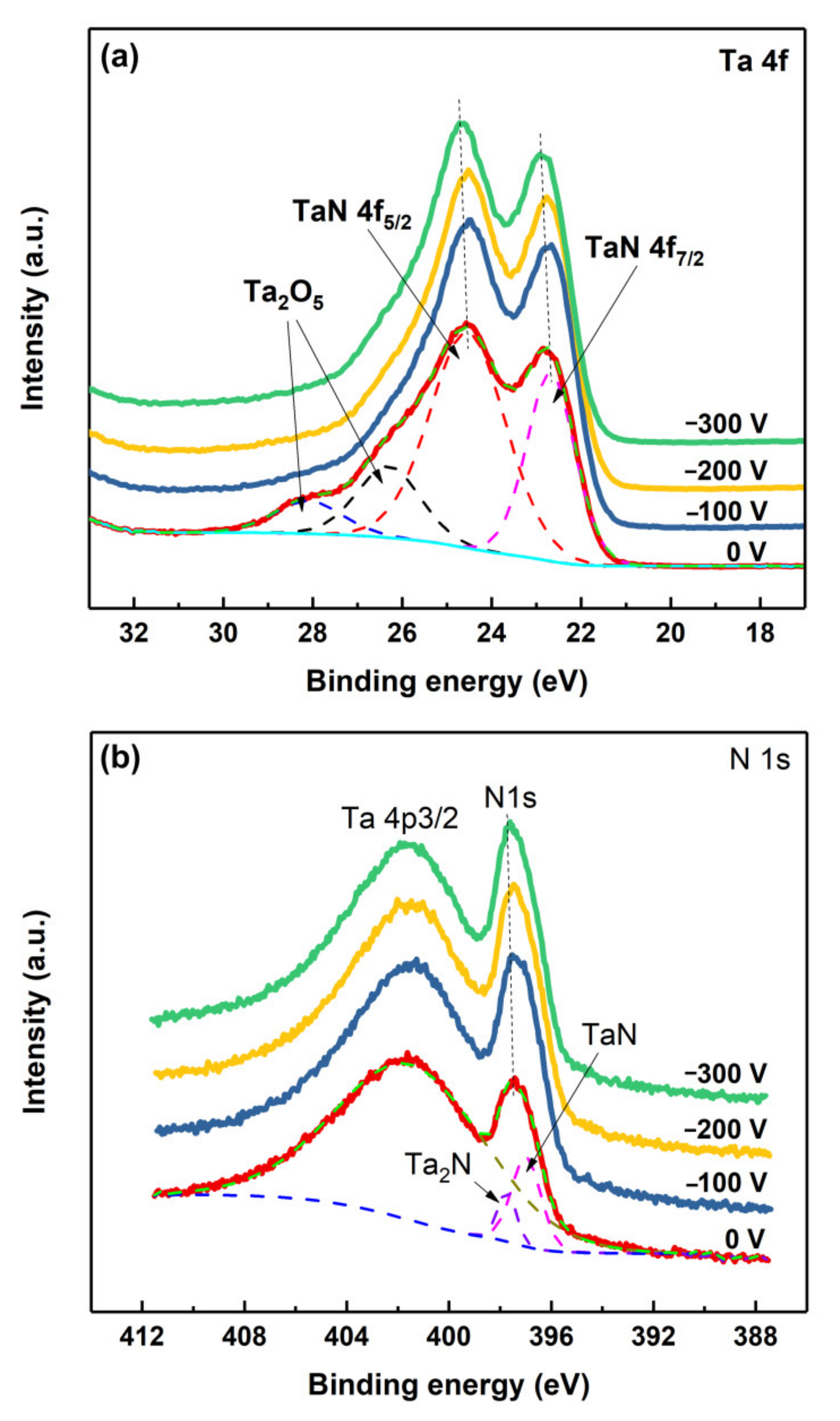
The surface chemical states of the coatings have been studied by XPS. The high-resolution XPS spectra for Ta 4f and N 1s are shown in
Figure 4a,b. The Ta 4f peak (
Figure 4a) can be deconvoluted into four peaks: Ta 4 f
7/2 peak (~22.7 eV), Ta 4 f
5/2 peak (~24.5 eV) and two peaks around 26.3 eV and 28.1 eV for Ta
2O
5 [
5,
12,
21]. As the bias voltage increases, the peaks of Ta in the Ta
2O
5 chemical state gradually weaken, which is consistent with the compositional analysis shown in
Figure 2. It should be noted that the bonding energies of the Ta 4 f
7/2 peaks (~22.7 eV) in the TaN
x coatings fall between that of the metallic Ta (Ta 4 f
7/2~21.7 eV) and that of the standard nitride (Ta 4f
7/2~23 eV), suggesting the formation of the Ta-N bonding in a low-stoichiometry (0 <
x < 1) chemical state. However, the result of the composition analysis above shows that the N/Ta ratio >1. Accordingly, it may be concluded that some N was implanted in Ta, i.e., Ta(N). As the bias voltage increases, both the Ta 4f
7/2 and Ta 4f
5/2 peaks shift to higher binding energy, indicating the transformation from the metal-rich state to the Ta-N bonding state. The high energy due to high bias voltage might facilitate the binding of Ta and N. The N 1s (
Figure 4b) spectra are also examined. The broad peak of the N 1s spectrum can be fitted with three peaks: the peak around 402 eV representing for Ta 4p
3/2 is almost constant, the peak centered at about 397 eV can be assigned to N in TaN, and the peak around 398 eV can be ascribed to N in Ta
2N. This depicts the presence of two binding states of TaN and Ta
2N, consistent with the results of the XRD analysis above. In addition, it is worth noting that as the bias voltage increases, the N 1s shows a slight shift to a higher binding energy, implying the increase of the Ta
2N fraction in the coatings. This also agrees well with the XRD results.
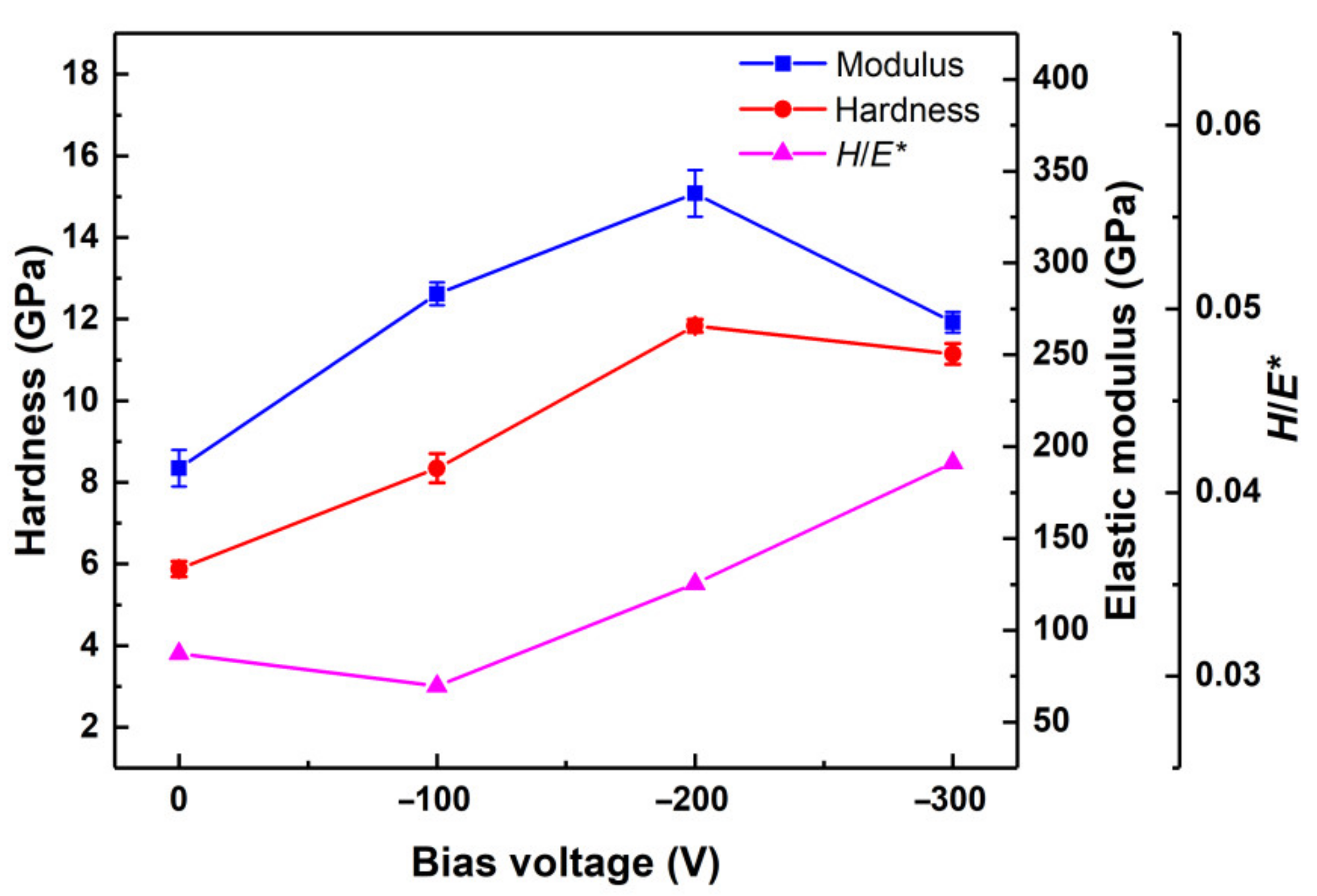
Figure 5 presents the hardness
H and the effective elastic modulus
E* of the TaN
x coatings deposited with various bias voltages. The hardness and elastic modulus of the coating deposited at 0 V are about 6 and 225 GPa, respectively. The relatively low values of hardness and elastic modulus might be attributed to the coarse and loosen structure of the coating deposited with relatively low bias voltage. The coating hardness and elastic modulus are increasing with increasing bias voltage, and reach a maximum at −200 V, and then decline when the bias voltage increases further. There are conflicting factors that influence the hardness and elastic modulus of the coatings. On the one hand, as the bias voltage increases, the coarse columnar crystal is refined and the coating structure becomes compact and dense, causing the improvement of the coating hardness and elastic modulus. Furthermore, it is reported that the Ta
2N phase has higher hardness than the TaN phase [
5,
22]. Accordingly, the increase of the Ta
2N phase fraction with bias voltage would contribute to the improvement of the TaN
x coatings. On the other hand, the coating structure gradually transfers into an amorphous structure, resulting in the decrease of the mechanical properties of the coatings. Accordingly, the coating hardness and elastic modulus tend to decrease when the bias voltage reaches −300 V where the TaN
x coating presents an amorphous structure, as identified by the XRD. The hardness
H and the effective elastic modulus
E* ratio
H/
E* are also presented in
Figure 5. It can be seen that the value of
H/
E* increases with the bias voltage except for −100 V where the coating shows the lowest
H/
E*. The increase of the
H/
E* might be attributed to the grain refinement of the coatings. High bias voltage would cause the coating structure to transfer to the zone T of the Thornton structure [
23], where the coating formed exhibit dense fibrous grains with a high
H/
E* ratio [
24]. The
H/
E* is believed to correlate with the elastic resilience and the resistance to plastic deformation, and a high
H/
E* is related to a high resistance to cracking, and hence, high fracture toughness, which is beneficial to the wear resistance of the coating [
25].
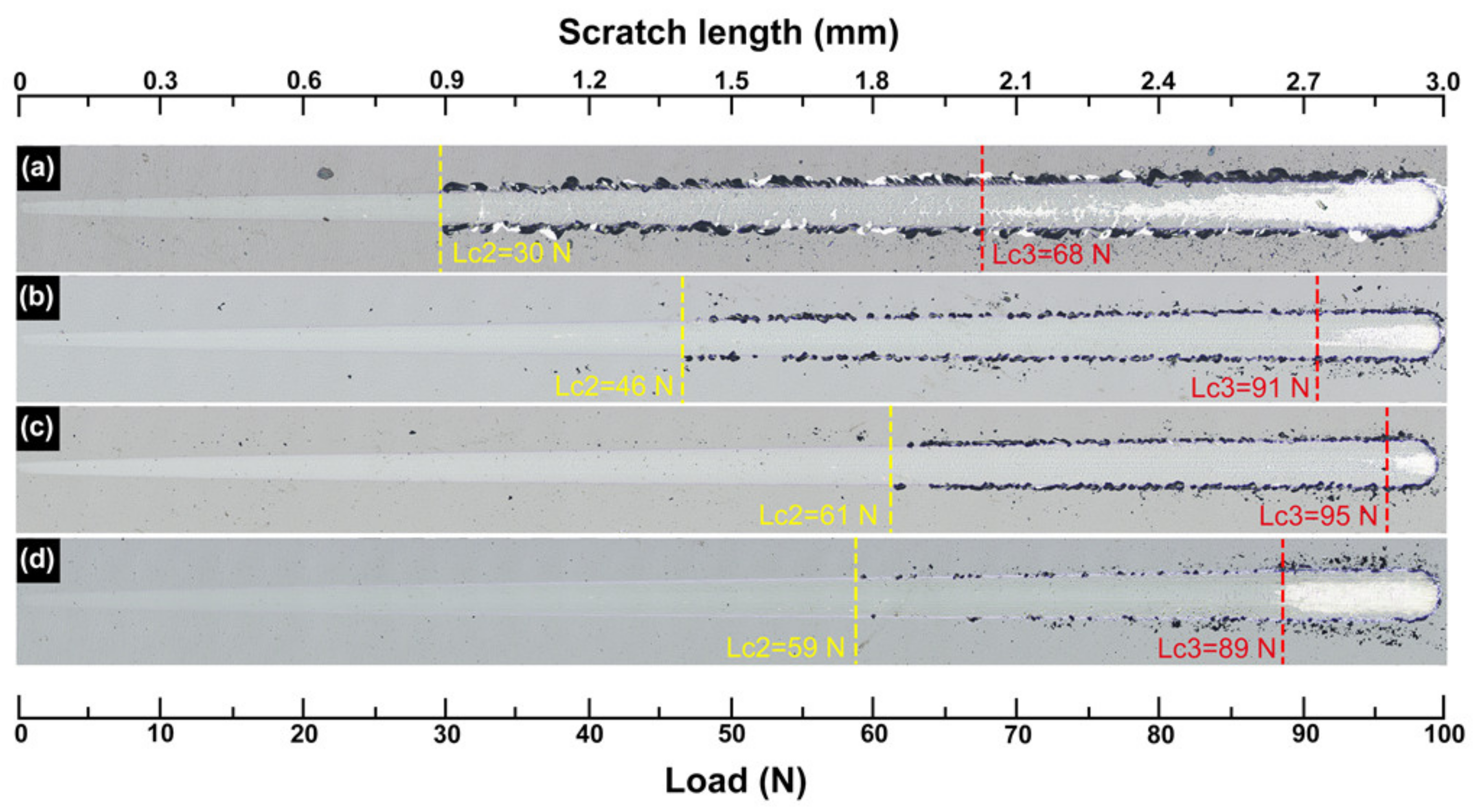
The adhesion strength of the deposited coatings was characterized through a scratch test. The images of the scratch tracks of the coatings after the scratch test are shown in
Figure 6. Usually, the critical load when the scratch begins to appear coating exfoliation (L
c2) is used to evaluate the coating-substrate bonding strength [
26]. It can be seen that, in general, the coatings deposited with bias voltage show a relatively higher L
c2 than that deposited without bias voltage (0 V). The TaN
x coating deposited at 0 V shows the L
c2 of about 30 N. As the bias voltage increases, the L
c2 of the coatings increases and reaches a maximum of about 61 N at –200 V. When the bias voltage increases further (−300 V), however, the L
c2 of the coating tends to decrease. It is clear that an increasing bias voltage is beneficial to the adhesion of the TaN
x coatings. Significantly, the chipping and fragmentation along the edges of the scratch tracks reduce dramatically with the bias voltage. In fact, besides the coating/substrate adhesion, the detachment of the fragments is also related to the cohesive (within the coating) fraction [
27]. As discussed above, the ratio
H/
E* of the coatings increases with increasing bias voltage, resulting in the enhancement of the coating toughness as well as the anti-scratch performance. The critical loads of the full delamination (L
c3) of the coatings are also included in
Figure 6. It can be seen that the variation of the L
c3 of the coatings is similar to the L
c2. The maximum value occurred at a bias voltage of −200 V, implying the best adhesion of the coating is deposited at −200 V among all samples. Then the L
c3 of the coating shows a small decrease when the bias voltage increases to −300 V. The decline of L
c3 might be attributed to the hardness decrease of the coating deposited at −300 V.
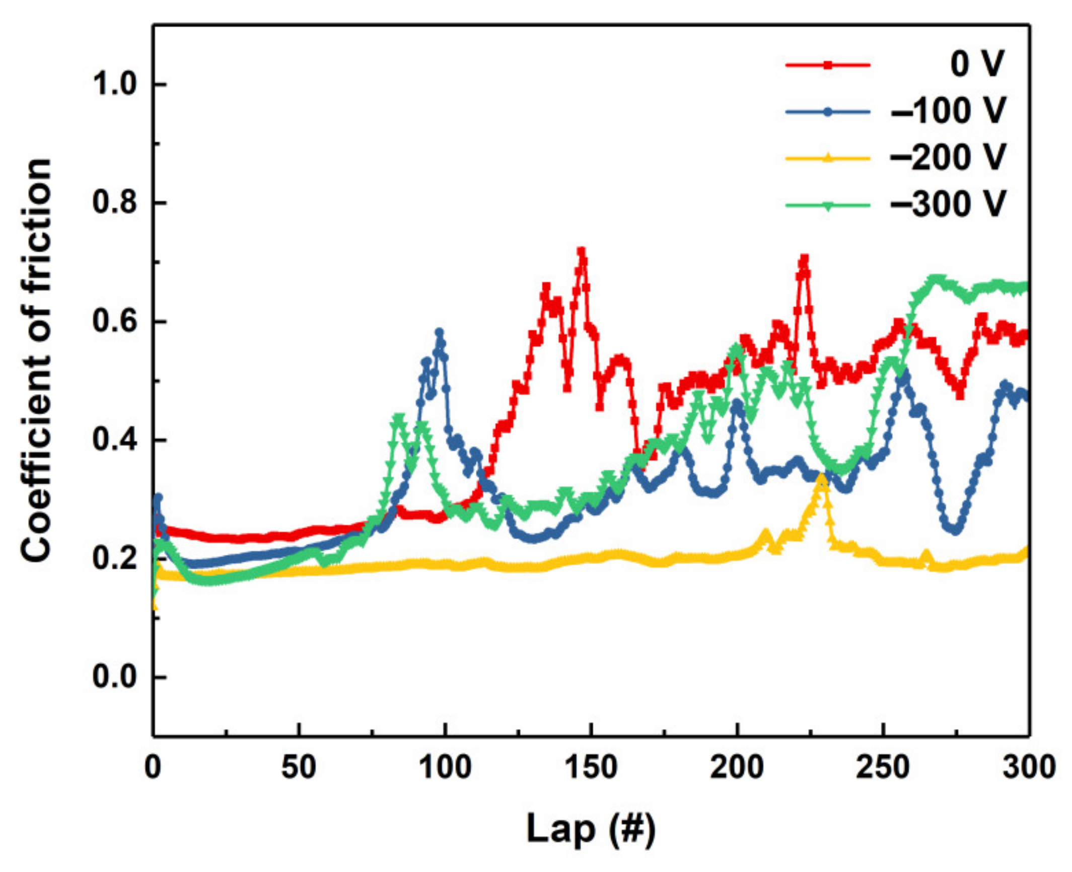
Tribological behaviors of the deposited TaN
x coatings deposited at different bias voltages were examined with the ball-on-disk wear tester.
Figure 7 presents the dynamic curves of the coefficients of friction (COFs) of the coatings as a function of friction test cycles. It can be seen that the coating deposited at −200 V presents a relative stable and smooth friction curve. The average COF is above 0.18, which is far lower than that of other PVD nitride hard coatings, e.g., CrN [
28], MoN and TiN [
29] which present COFs > 0.3. For the coatings deposited with other bias voltages, the friction process can be divided into two stages after the running-in process. In the initial stage (lap < 70 cycles), all the samples show stable and low COF curves. The coatings deposited with −200 and −300 V present the lowest COF among these samples. In addition, the coating deposited at 0 V shows the maximum COF. As the lap excesses 70 cycles, however, the friction process becomes unstable and the COF curers start to oscillate. In addition, the corresponding COFs of the coatings increase to about 0.4.
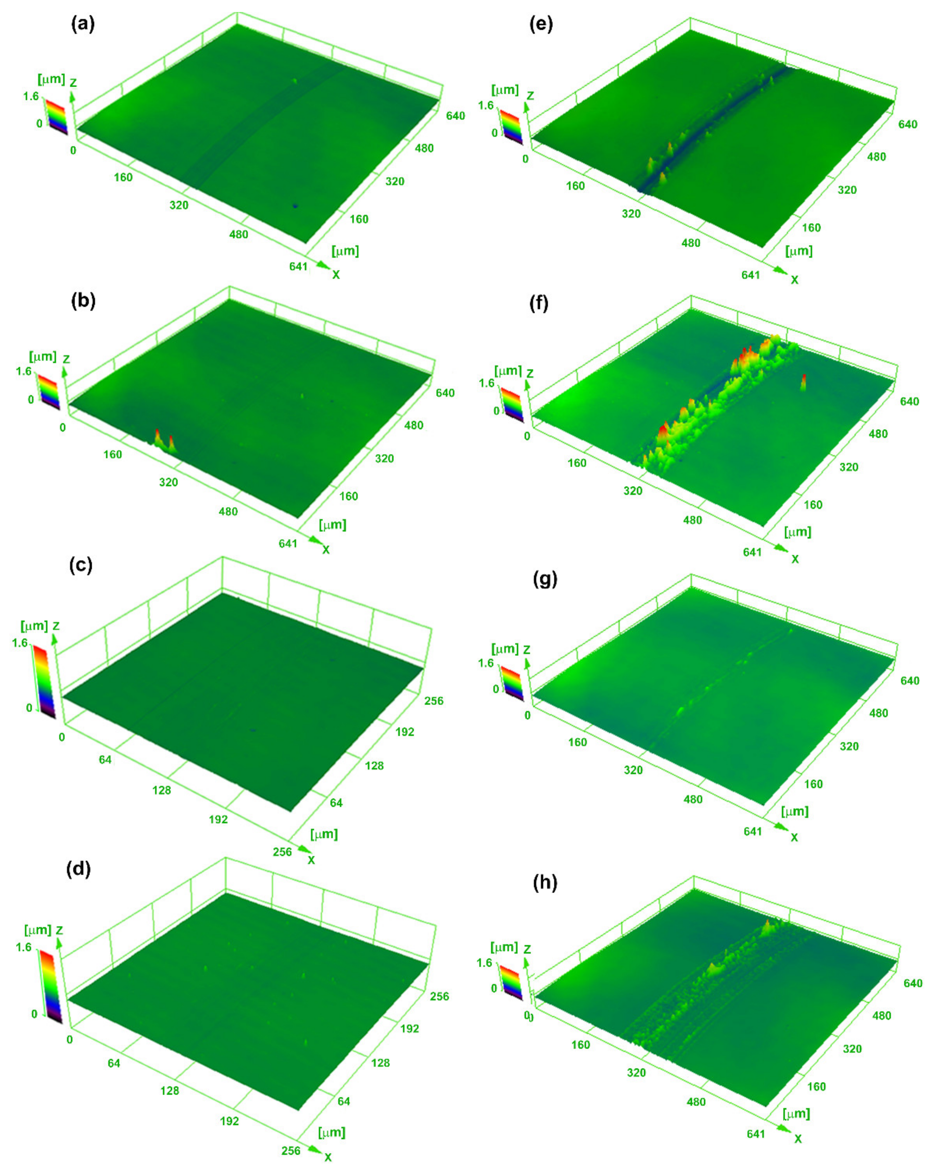
The wear tracks of the samples after friction tests with 60 cycles are shown in
Figure 8a–d. It should be noted that all the coatings show relatively low and smooth tracks. The wear track of the coating deposited at 0 V (
Figure 8a) is deeper than that of the coatings deposited with other bias voltages, illustrating the relative higher wear rate of the coating deposited at 0 V. As the friction lap increases to 300 cycles, the wear depths of the coating increase (
Figure 8e–h). It is worth noting that there is a large amount of wear debris adhered to the wear tracks on the coatings deposited at 0 and −100 V. The adherent debris might be the main reason that causes the oscillation of the friction process, as shown in the dynamic curves in
Figure 7 when the lap excesses 70 cycles. For the coating deposited with −200 V, however, the adherent debris tends to decrease and the wear track becomes shallow and narrow, implying the enhanced wear resistance of the coating. However, the wear width of the coating increases significantly when the bias voltage increases further (−300 V).
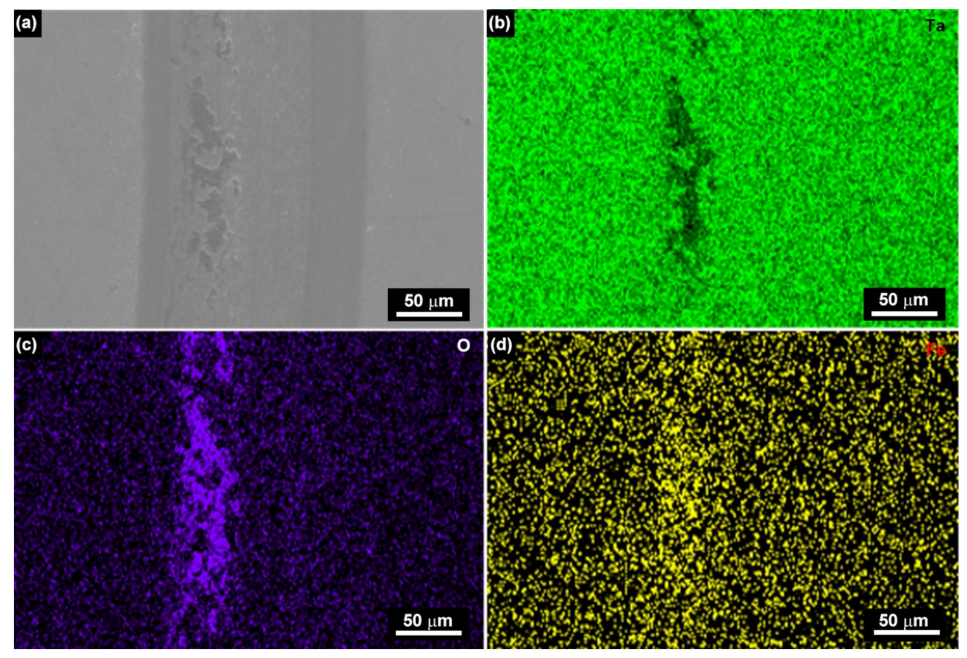
Figure 9 shows a typical SEM image and the corresponding EDX mapping of the wear track of the coating deposited at −100 V. It can be seen that the wear debris adhered to the wear tracks is mainly composed of Fe (
Figure 9d) and O (
Figure 9c), illustrating that the wear debris was dominantly transferred from the friction SU304 ball. The relative soft SU304 can be worn away by the hard coatings. In addition, the Ta element cannot be detected in the wear track (as shown in
Figure 9b), indicating that the coating peeling occurred on the wear track. The coating chipping would cause seriously abrasive wear. Accordingly, the coating deposited at −100 V exhibits a poor tribological performance.
The tribological performances of the coatings are believed to have a relationship with the composition and microstructure of the coatings. The high wear rate and COF of the coatings deposited at relative lower bias voltages (0 and −100 V) could be attributed to the presence of both TaN and Ta
2N phases, which can cause a three-body wear (e.g., the adherent wear debris) at the contact resulting in the faster wear rate [
5]. In addition, the relatively low hardness and toughness (
H/
E*) of the coatings also decrease the wear resistance, and the coarse surface would enhance the adhesion of the wear debris. On the contrary, the coating deposited at a relatively high bias voltage (−200 V) has a uniform microstructure that is composed of a Ta
2N phase present as fine columnar grains with enhanced hardness and smooth surface. The enhanced hardness and compact surface structure could increase the wear resistance and reduce the adhesion of the wear debris. As a result, the TaN
x coating deposited at −200 V shows a good tribological performance with low wear rate and COF. It is believed that the Ta
2N coating can serve as a potential coating material for tribological applications. However, the coating transfers into an amorphous structure as the bias voltage increases to −300 V, causing the coating hardness to decease and then resulting in the reduction of the wear resistance.


