
Effect of Substrate Biasing on the Epitaxial Growth and Structural Properties of RF Magnetron Sputtered Germanium Buffer Layer on Silicon


Abstract
:1. Introduction
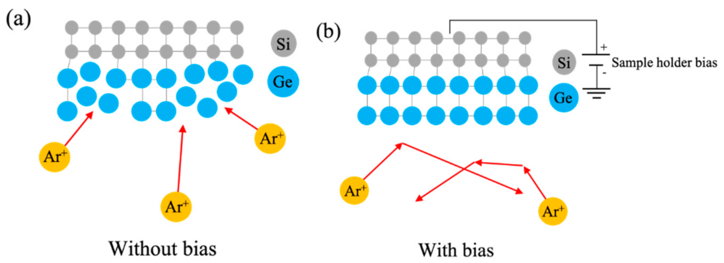
2. Experiments
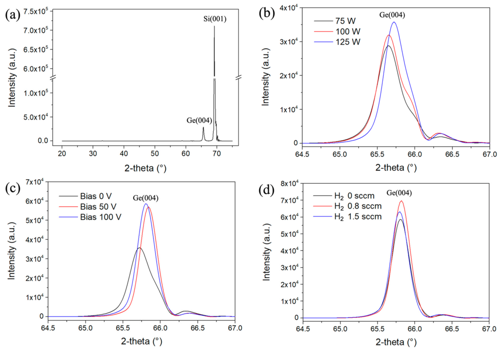
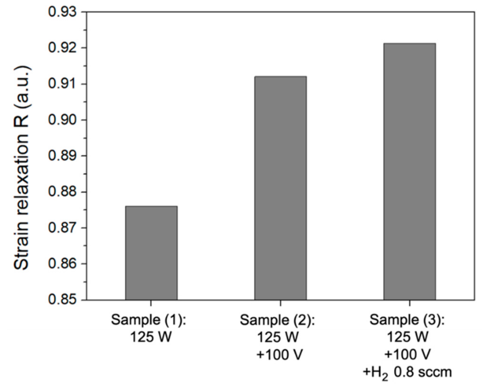
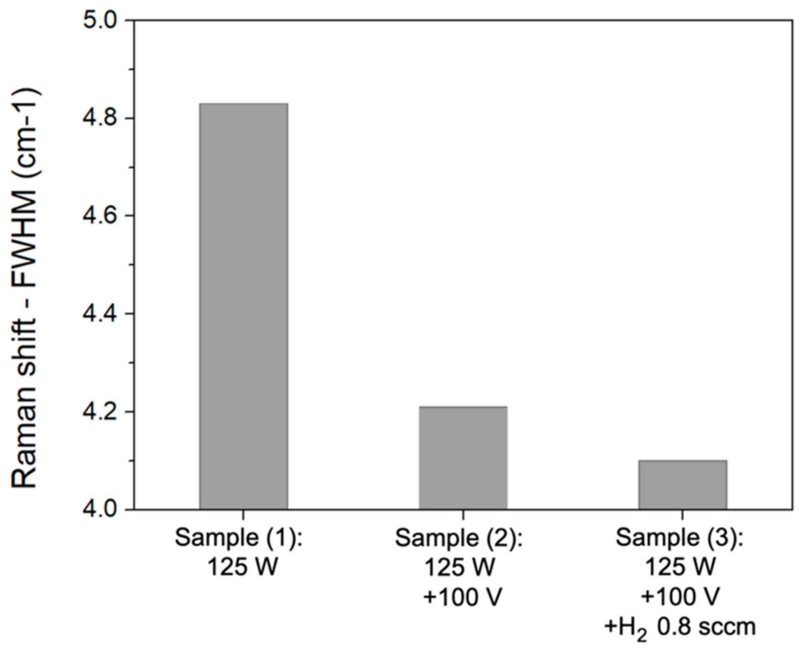
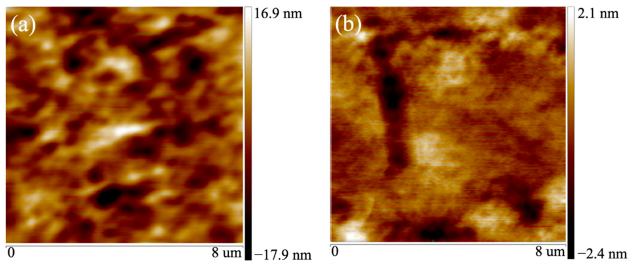
3. Results and Analysis
4. Conclusions
Author Contributions
Funding
Institutional Review Board Statement
Informed Consent Statement
Conflicts of Interest
References
- Luque, A. Will we exceed 50% efficiency in photovoltaics? J. Appl. Phys. 2011, 110, 031301. [Google Scholar] [CrossRef]
- Yoon, H.; Granata, J.E.; Hebert, P.; King, R.R.; Fetzer, C.M.; Colter, P.C.; Edmondson, K.M.; Law, D.; Kinsey, G.S.; Krut, D.D.; et al. Recent advances in high-efficiency III-V multi-junction solar cells for space applications: Ultra triple junction qualification. Prog. Photovolt Res. Appl. 2005, 13, 133–139. [Google Scholar] [CrossRef]
- Cansizoglu, H.; Bartolo-Perez, C.; Gao, Y.; Devine, E.P.; Ghandiparsi, S.; Polat, K.G.; Mamtaz, H.H.; Yamada, T.; Elrefaie, A.F.; Wang, S.Y.; et al. Surface-illuminated photon-trapping high-speed Ge-on-Si photodiodes with improved efficiency up to 1700 nm. Photon. Res. 2018, 6, 734–742. [Google Scholar] [CrossRef]
- Suh, D.; Kim, S.; Joo, J.; Kim, G. 36-GHz high-responsivity Ge photodetectors grown by RPCVD. IEEE Photon. Tech. Lett. 2009, 21, 672–674. [Google Scholar]
- Colace, L.; Assanto, G. Ge on Si for near-infrared light sensing. IEEE Photonics J. 2009, 1, 69–79. [Google Scholar] [CrossRef]
- Horowitz, K.A.W.; Woodhouse, M.; Lee, H.; Smestad, G. A bottom-up cost analysis of a high concentration PV module. AIP Conf. Proc. 2015, 1679, 100001. [Google Scholar]
- Littlejohns, C.G.; Khokhar, A.Z.; Thomson, D.J.; Hu, Y.; Basset, L.; Reynolds, S.A.; Mashanovich, G.Z.; Reed, G.T.; Gardes, F.Y. Ge-on-Si plasma-enhanced chemical vapor deposition for low-cost photodetectors. IEEE Photonics J. 2015, 7, 1–8. [Google Scholar] [CrossRef]
- Yamamoto, Y.; Zaumseil, P.; Arguirov, T.; Kittler, M.; Tillack, B. Low threading dislocation density Ge deposited on Si (100) using RPCVD. Solid State Electron. 2011, 60, 2–6. [Google Scholar] [CrossRef]
- Du, Y.; Kong, Z.; Toprak, M.S.; Wang, G.; Miao, Y.; Xu, B.; Yu, J.; Li, B.; Lin, H.; Han, J.; et al. Investigation of the heteroepitaxial process optimization of Ge layers on Si (001) by Rpcvd. Nanomaterials 2021, 11, 928. [Google Scholar] [CrossRef]
- Kuo, W.C.; Lin, C.Y.; Lee, C.C.; Cheng, C.C.; Chang, J.Y. Strain-Controlled of Compressive/Tensile Ge epilayers on Si by electron cyclotron resonance chemical vapor deposition. ECS J. Solid State Sci. Technol. 2016, 5, 529–533. [Google Scholar] [CrossRef]
- Sorianello, V.; Colace, L.; Armani, N.; Rossi, F.; Ferrari, C.; Lazzarini, L.; Assanto, G. Low-temperature germanium thin films on silicon. Opt. Mater. Express. 2011, 1, 856–865. [Google Scholar] [CrossRef] [Green Version]
- Li, H.S.; Qiu, F.; Xin, Z.H.; Wang, R.F.; Yang, J.; Zhang, J.; Wang, C.; Yang, Y. Investigation of the microstructure and optical properties of Ge films grown by DC magnetron sputtering and in situ annealing. Jpn. J. Appl. Phys. 2016, 55, 061302. [Google Scholar] [CrossRef]
- Liu, Z.H.; Hao, X.J.; Huang, J.L.; Li, W.; Ho-Baillie, A.; Green, M.A. Diode laser annealing on Ge/Si (100) epitaxial films grown by magnetron sputtering. Thin Solid Films 2016, 609, 49–52. [Google Scholar] [CrossRef]
- Raisknen, J.; Hirvonen, J.; Anitila, A. The diffusion of silicon in germanium. Solid State Electron. 1981, 24, 333–336. [Google Scholar] [CrossRef]
- Pan, T.M.; Lei, T.F.; Chao, T.S.; Liaw, M.C.; Ko, F.H.; Lu, C.P. One-step cleaning solution to replace the conventional RCA two-step cleaning recipe for pregate oxide cleaning. J. Electrochem. Soc. 2001, 148, G315–G320. [Google Scholar] [CrossRef]
- Miyata, S.; Toyoda, R.; Hashimoto, M.; Iijima, T.; Tonegawa, A.; Matsumura, Y. Effect of sputtering gas ions on thin film properties. J. Japan Inst. Met. Mater. 2016, 80, 280–283. [Google Scholar] [CrossRef] [Green Version]
- Oh, J.; Banerjee, S.K.; Campbell, J.C. Metal–Ge–Metal photodetectors on heteroepitaxial Ge-on-Si with amorphous Ge schottky barrier enhancement layers. IEEE Photon. Tech. Lett. 2004, 16, 581–583. [Google Scholar] [CrossRef]
- Lee, K.H.; Jandl, A.; Tan, Y.H.; Fitzgerald, E.A.; Tan, C.S. Growth and characterization of Ge epitaxial film on Si (001) with germane precursor in metal organic chemical vapour deposition (MOCVD) chamber. AIP Adv. 2013, 3, 092123. [Google Scholar] [CrossRef]
- Yokomichi, H.; Morigaki, K. Evidence for existence of hydrogen-related dangling bonds in hydrogenated amorphous Si. Phil. Mag. Lett. 1996, 73, 283–287. [Google Scholar] [CrossRef]
- Beyer, W.; Herion, J.; Wagner, H.; Zastrow, U. Hydrogen stability in amorphous Ge films. Philos. Mag. Part B 1991, 63, 269–279. [Google Scholar] [CrossRef]
- Nakamura, K.; Yoshino, K.; Takeoka, S.; Shimizu, I. Roles of atomic hydrogen in chemical annealing. Jpn. J. Appl. Phys. 1995, 34, 442–449. [Google Scholar] [CrossRef]
- Liu, Z.; Hao, X.; Ho-Baillie, A.; Tsao, C.Y.; Green, M.A. Cyclic thermal annealing on Ge/Si(100) epitaxial films grown by magnetron sputtering. Thin Solid Films 2015, 574, 99–102. [Google Scholar] [CrossRef]
- Miyata, Y.; Ueno, K.; Yoshimura, T.; Ashida, A.; Fujimura, N. Cerium ion doping into self-assembled Ge using three-dimensional dot structure. J. Cryst. Growth 2017, 468, 696–700. [Google Scholar] [CrossRef]
- Truong, Q.D.; Devaraju, M.K.; Tomai, T.; Honma, I. Direct Observation of Antisite Defects in LiCoPO4 Cathode Materials by Annular Dark and Bright Field Electron Microscopy. ACS Appl. Mater. Interfaces 2013, 5, 9926–9932. [Google Scholar] [CrossRef]
- Toko, K.; Nakazawa, K.; Saitoh, N.; Yoshizawa, N.; Suemasu, T. Improved surface quality of the metal-induced crystallized Ge seed layer and its influence on subsequent epitaxy. Cryst. Growth Des. 2015, 15, 1535–1539. [Google Scholar] [CrossRef]
- Dos Santos, D.R.; Torriani, I.L. Crystallite size determination in Mu-C-GE films by X-Ray-Diffraction and raman line-profile analysis. Solid State Comm. 1993, 85, 307–310. [Google Scholar] [CrossRef]
- Jain, J.R.; Ly-Gagnon, D.-S.; Balram, K.C.; White, J.S.; Brongersma, M.L.; Miller, D.A.B.; Howe, R.T. Tensile-strained germanium-on-insulator substrate fabrication for silicon-compatible optoelectronics. Opt. Mater. Express. 2011, 1, 1121–1126. [Google Scholar] [CrossRef] [Green Version]


| Process Equipment | Year | Temp (°C) | Thickness (nm) | Annealing Temp (°C) | XRD/FWHM (arcsec) | AFM/RMS (nm) | Ref. |
|---|---|---|---|---|---|---|---|
| PECVD | 2015 | 400/250 | 705 | 600 | 1012 | 3.5 | [7] |
| RPCVD | 2011 | 550/300 | 4700 | 800 | 41.76 | 0.44 | [8] |
| RPCVD | 2021 | 650/400 | 1400 | 820 | 131 | 0.81 | [9] |
| ECR-CVD | 2016 | 220 | 100 | - | 532 | 1.5 | [10] |
| Thermal Evaporation | 2011 | 300 | 200 | - | 1188 | - | [11] |
| DC-Sputtering | 2016 | 450 | 300 | 750 | - | 4.6 | [12] |
| RF-Sputtering | 2016 | 400 | 400 | 910 | 1260 | - | [13] |
| Process Parameters | Sample Center RMS (nm) | Sample Edge RMS (nm) |
|---|---|---|
| Sample (1): 125 W | 4.94 | 1.04 |
| Sample (2): 125 W + 100 V | 0.58 | 0.42 |
| Sample (3): 125 W+100 V + H2 0.8 sccm | 0.81 | 0.61 |
Publisher’s Note: MDPI stays neutral with regard to jurisdictional claims in published maps and institutional affiliations. |
© 2021 by the authors. Licensee MDPI, Basel, Switzerland. This article is an open access article distributed under the terms and conditions of the Creative Commons Attribution (CC BY) license (https://creativecommons.org/licenses/by/4.0/).
Share and Cite
Zeng, G.-S.; Liu, C.-L.; Chen, S.-H. Effect of Substrate Biasing on the Epitaxial Growth and Structural Properties of RF Magnetron Sputtered Germanium Buffer Layer on Silicon. Coatings 2021, 11, 1060. https://doi.org/10.3390/coatings11091060
Zeng G-S, Liu C-L, Chen S-H. Effect of Substrate Biasing on the Epitaxial Growth and Structural Properties of RF Magnetron Sputtered Germanium Buffer Layer on Silicon. Coatings. 2021; 11(9):1060. https://doi.org/10.3390/coatings11091060
Chicago/Turabian StyleZeng, Gui-Sheng, Chi-Lung Liu, and Sheng-Hui Chen. 2021. "Effect of Substrate Biasing on the Epitaxial Growth and Structural Properties of RF Magnetron Sputtered Germanium Buffer Layer on Silicon" Coatings 11, no. 9: 1060. https://doi.org/10.3390/coatings11091060
APA StyleZeng, G.-S., Liu, C.-L., & Chen, S.-H. (2021). Effect of Substrate Biasing on the Epitaxial Growth and Structural Properties of RF Magnetron Sputtered Germanium Buffer Layer on Silicon. Coatings, 11(9), 1060. https://doi.org/10.3390/coatings11091060