Abstract
We report the growth of non-polar GaN and AlGaN films on Si(111) substrates by plasma-assisted metal-organic chemical vapor deposition (PA-MOCVD). Low-temperature growth of GaN or AlN was used as a buffer layer to overcome the lattice mismatch and thermal expansion coefficient between GaN and Si(111) and GaN’s poor wetting on Si(111). As grown, the buffer layer is amorphous, and it crystalizes during annealing to the growth temperature and then serves as a template for the growth of GaN or AlGaN. We used scanning electron microscopy (SEM), atomic force microscopy (AFM), and X-ray diffraction (XRD) characterization to investigate the influence of the buffer layer on crystal structure, orientation, and the morphology of GaN. We found that the GaN buffer layer is superior to the AlN buffer layer. The thickness of the GaN buffer layer played a critical role in the crystal quality and plane orientation and in reducing the cracks during the growth of GaN/Si(111) layers. The optimum GaN buffer layer thickness is around 50 nm, and by using the optimized GaN buffer layer, we investigated the growth of AlGaN with varying Al compositions. The morphology of the AlGaN films is flat and homogenous, with less than 1 nm surface roughness, and has preferred orientation in a-axis.
1. Introduction
The unique properties of GaN and related III-nitrides, such as direct wide-bandgap, high thermal stability, and high voltage breakdown, have attracted interest. These properties make them suitable for use as visible and ultraviolet optoelectronic devices and high-power and high-frequency electronic devices [1,2,3]. GaN-based devices are usually made on sapphire substrates and grown in a c-axis oriented wurtzite epilayer using various techniques such as molecular-beam epitaxy (MBE) and MOCVD. However, using sapphire substrate in GaN-based devices has raised several problems associated with the sapphire substrates. First, sapphire has a low thermal conductivity, making it difficult to transfer heat [4]. As a result, heat generated in GaN-based devices with sapphire as a substrate cannot be dissipated quickly, causing degrading device performance and shortening of a lifetime. Secondly, internal spontaneous and piezoelectric polarization processes in GaN-based heterostructures can generate a significant electric field at the nitrides interface causes increasing the radiative lifetime [5] and lowering quantum efficiency [6].
There are two approaches to resolve the polarization problem. One option is to use cubic GaN, which is non-polar in the cubic [001] direction, thus avoiding polarization-induced electric fields at heterointerfaces. Unfortunately, cubic GaN is metastable, and producing it is challenging. The alternative option is to use hexagonal GaN in the a- or m-plane rather than the c-plane, which is known as non-polar GaN such as and planes [7,8]. There is no polarization-induced electric field in nitrides interfaces for this type of orientated GaN; therefore, non-polar GaN materials are advantageous for attaining high internal quantum efficiency [9,10].
Non-polar GaN has been grown on various substrates with or without interlayer by various techniques. Silicon substrate is attractive because it is inexpensive and available in large sizes, making it excellent for fabricating low-cost GaN-based devices. In particular, Si(111) is widely used as a substrate for the growth of c-axis oriented GaN-based devices due to the excellent match of hexagonal GaN with the threefold surface symmetry of Si(111). Other silicon substrate types have also been shown to be suitable for the growth of GaN on Si, such as Si(001) and Si(110) [11,12]. However, to date, only a few studies have used Si(111) as a substrate for the growth of non-polar GaN.
Compared to sapphire, silicon has some advantages, such as it poses higher thermal conductivity, which is four times greater than sapphire [13]. As a result, GaN-based devices fabricated on Si(111) substrates will have superior heat dissipation. However, the growth of heteroepitaxial GaN on Si raises several challenges, such as significant mismatches in the lattice parameter and thermal expansion coefficient between GaN and Si substrates [14,15]. Another problem is GaN’s poor wetting on Si(111), which prevents direct nucleation that typically leads to poor GaN morphology and crystal quality [16]. These are similar to that encountered in the heteroepitaxial growth of GaAs on Si. In that case, using an amorphous GaAs buffer layer leads to a better-quality GaAs epilayer [17].
MOCVD is a well-known technique for growing GaN for optoelectronic and electronic devices applications. Thermal MOCVD involves cracking NH3 as a nitrogen source and reacting it with trimethyl/tetraethylgallium (TMGa/TEGa) as a gallium source at a high temperature (in the vicinity of 1100 °C). Such high temperatures may create issues, such as atomic diffusion and thermal expansion during the cooling process that leads to difficulty obtaining crack-free GaN layers. Many approaches to reduce cracks and improve crystal quality have been reported, including using a step-graded AlGaN interlayer [18], AlN/GaN superlattice [19], and low-temperature AlN (LT-AlN) interlayer [20]. However, as compared to GaN grown on a sapphire substrate, these approaches have not produced a perfect crack-free GaN/Si(111) epitaxy.
Since using such high temperatures in the MOCVD technique raises some problems, we propose a plasma-assisted MOCVD technique to grow non-polar AlGaN on a Si(111) substrate in this study. Plasma-assisted MOCVD employs microwave radiation to generate reactive nitrogen plasma that can react with gallium at a significantly low temperature of around 700 °C [21]. Due to the varied crystallographic orientations, the growth conditions for non-polar GaN materials differ from those for c-plane GaN. Here we study and optimize the effect of GaN and AlN buffer layer thickness on the GaN and AlGaN crystallites orientation and morphology. The buffer layer was grown at low temperatures resulting in amorphous GaN or AlN, which crystallized during the temperature ramp to the growth temperature and maintained the temperature for 20 min. The crystallized GaN and AlN then serve as a template for GaN and AlGaN growth.
2. Materials and Methods
Experimental detail of GaN and AlGaN growth is similar to that described in [21]. A high purity (99.999%) nitrogen gas was used and transported to the reactor (home-built) through a downstream cavity type of 2.45 GHz ECR plasma source (ASTeX) to produce nitrogen plasma. Trimethylgallium (TMGa) was used as a gallium source, while the reactive nitrogen species from nitrogen plasma were used as a nitrogen source. Hydrogen gas was used as carrier gas and was purified by passing it through a heated palladium cell.
The Si(111) substrates were chemically cleaned using the RCA procedure, and they were immediately loaded into the reactor and heated up to 650 °C for thermal cleaning in the H2 ambient. In-situ hydrogen plasma cleaning of the substrates was carried out for 10 min using 200 watts plasma power with the H2 flow rate of 50 sccm. The temperature was then decreased to 500–550 °C to grow GaN or AlN buffer layer with TMGa flow rate of 0.12 sccm and N2 flow rate of 90 sccm.
The experiment started with investigating the effect of GaN and Al buffer layer thickness on the structural and morphology characteristics of GaN. The buffer layer was grown for 5–15 min, resulting in buffer layers with thicknesses of around 16–50 nm. According to our routine growth process, GaN or AlN layers grown at 500–550 °C are amorphous. After the buffer layer was deposited, the substrate temperature was slowly ramped to 680 °C. The amorphous buffer layer underwent a crystallization process during the temperature ramp to 680 °C and was maintained for about 20 min. On top of the buffer layer, GaN film was grown for 2 h using TMGa and a nitrogen flow rate of around 0.1 and 90 sccm, respectively.
We characterized the structural and morphology properties of the grown GaN and determined the optimized buffer layer thickness. Based on the optimized buffer layer thickness obtained from the growth of GaN, we grew AlGaN with variations in the flow rate of TMAl/(TMAl + TMGa) of 10%–40% with a V/III ratio of 650 at a growth temperature of 700 °C. The growth temperature is somewhat higher than that of GaN film because TMGa has a higher vapor pressure than TMAl at the same temperature. As a result, AlGaN thin films require a higher growth temperature than GaN thin films. The crystallographic structure of GaN and AlGaN films was investigated by XRD (Philips, PW3710, Almelo, The Netherlands), while SEM (JEOL, JSM-6510LA, Tokyo, Japan) and AFM (Seiko Instruments, SPA-400, Chiba, Japan) were used to examine the surface morphology of the samples. The atomic composition of the films was determined using an energy dispersive X-ray analyzer (EDS), integrated with SEM.
3. Results
3.1. Growth of GaN
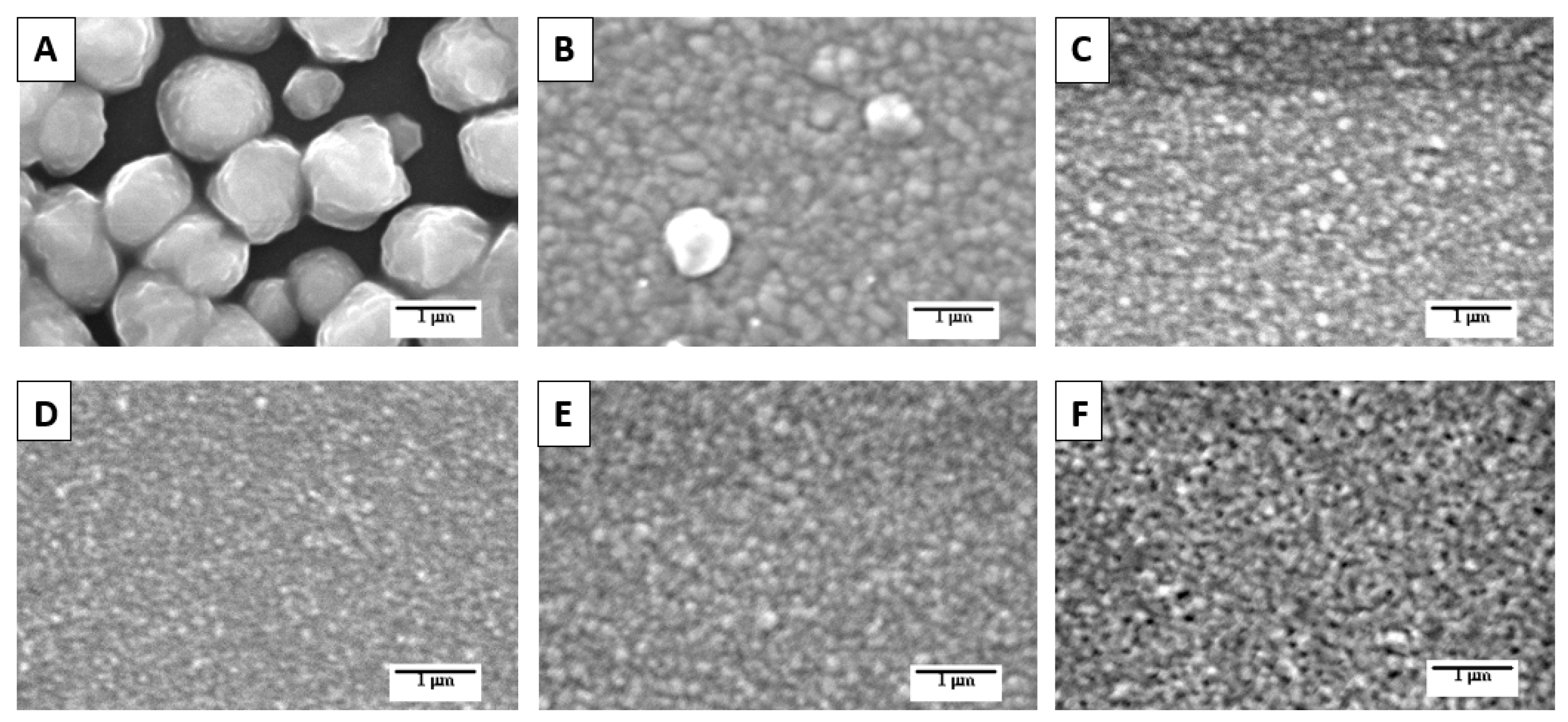
GaN films were grown directly on top of a low-temperature growth of GaN or AlN buffer layer. The buffer layer was deposited with different growth times, resulting in different GaN and AlN thicknesses. Table 1 shows the thickness of each buffer layer, which was estimated from cross-sectional SEM measurements of the thicker buffer layer. The other buffer layers thicknesses were deduced from the growth time assuming a constant growth rate. Figure 1 shows the surface morphology of GaN films grown with and without a buffer layer. The morphology of GaN without a buffer layer (sample A) appears to be dominated by hexagonal islands separated by about 0.2–0.6 μm. The island separation indicates a non-uniform three-dimensional growth mode, and nucleation dispersion occurs, resulting in a partial covering of the substrate surface. This type of growth mode is most likely due to a lattice mismatch between GaN and the Si substrate and a significant divergence in interfacial energy between GaN and Si. Therefore, the growth of GaN film directly on top of Si results in the nucleation of separate islands. The formation of separated grain islands suggests that the nucleation rate is substantially low.

Table 1.
Buffer layer thickness and Ga/N atomic ratio of GaN films grown with different buffer layer thicknesses.
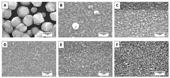
Figure 1.
SEM images of the surface morphology of GaN films grown on Si(111) with different buffer layer thicknesses. (A) (without buffer layer), (B–D) (GaN buffer layer, with thicknesses of 16, 33, and 50 nm, respectively), (E,F) (AlN buffer layer with thicknesses of 29 and 44 nm).
In the heteroepitaxy process, the nucleation process plays an important role. Because of the structural and chemical incompatibilities between GaN and Si, growing GaN directly on Si substrate is difficult. The nitridation of the Si surface could be one cause for the poor wetting of GaN deposition on Si. If MOCVD is used with NH3 as a nitrogen source, Si will easily react with NH3 at temperatures above 500 °C to form Si3N4 [22] during the annealing process. Consequently, nitridation problems can be avoided using an ammonia-free atmosphere during the first growth stage. Therefore, we use plasma nitrogen to cover Si substrate with low-temperature growth amorphous GaN layer to minimize this nitridation process. This technique is expected to increase GaN wetting on Si and provide a homogeneous surface for GaN upper growth.
Figure 1B–F shows the morphology of GaN films deposited with various buffer layers thickness. According to the SEM results, GaN film morphologies depend significantly on the thickness of the buffer layer. As the GaN film was grown with a buffer layer, either GaN or AlN (samples B to F), almost homogeneous grains (~0.05 μm in size) are formed, demonstrating lateral growth occurs. These findings suggest that the buffer layer effectively reduces the interfacial energy between the substrate and the GaN film, allowing for a faster coalition process between islands, as evidenced by the smaller grain size formed.
SEM images of samples B to D show that the grain size becomes smaller as the thickness of the buffer layer increases. That means the thicker the buffer layer, the faster the nucleation between grains occurred. The growth of the buffer layer at a low temperature produces an amorphous layer that accommodates the increase of strains due to the differences in lattice constants through the crystallization process during annealing the buffer layer at the growth temperature of the GaN film. Similar results are also observed by Chen et al., that growth of GaN buffer layer deposited at 300 °C, resulting in amorphous GaN that begins to crystallize at 500 °C [23]. When the buffer layer is grown at a low temperature, the supersaturation of the organic metal precursor TMGa is high enough to provide an increase in the chemical driving force for the formation of GaN and subsequently results in a high nucleation rate. In addition, from the results of SEM images, the surface morphology of GaN thin films grown with GaN or AlN buffer layers does not have crack patterns on the film surface, indicating that the buffer layer can reduce the strain that occurs between the substrate and the film.
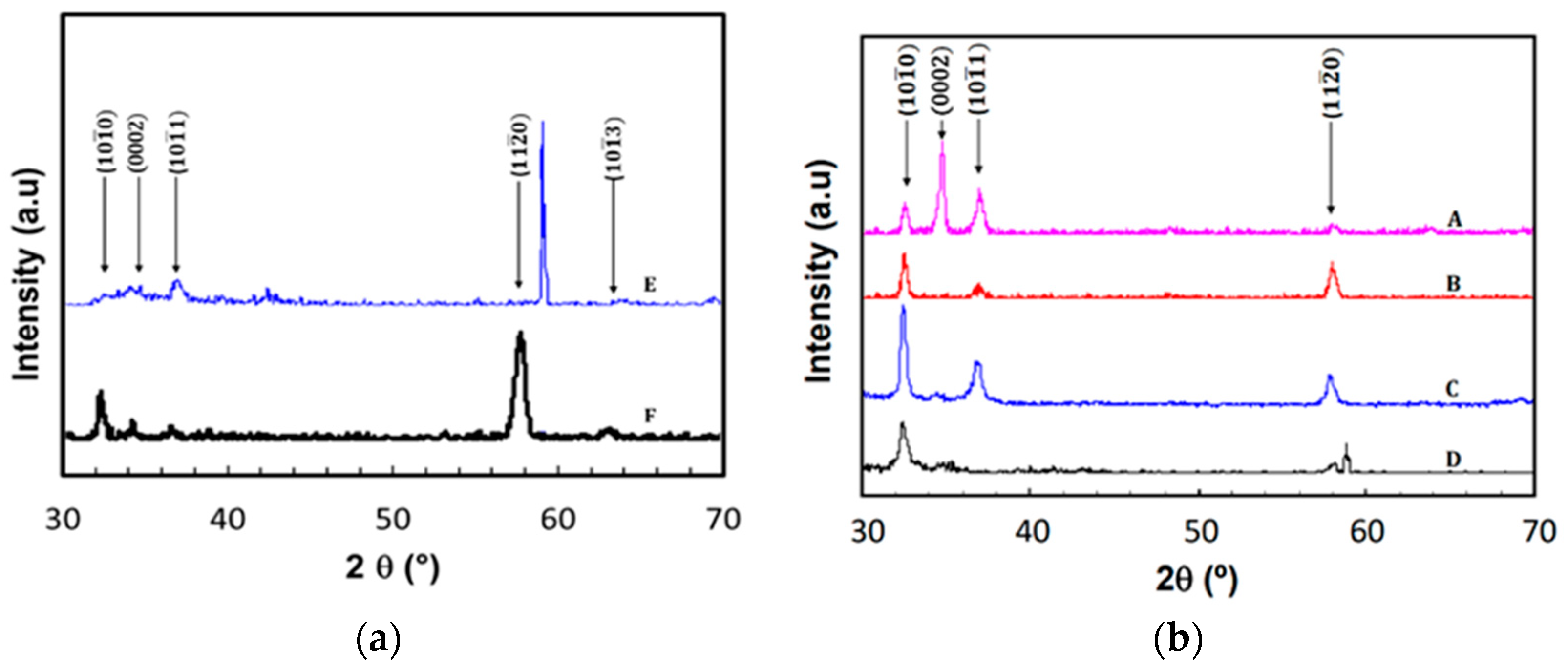
We explored the influence of buffer layer thickness on the crystal structure of the GaN films deposited on top of it to understand better the role of the buffer layer on the crystal structure. Figure 2 shows the XRD diffraction pattern of the grown GaN films with the GaN buffer layer thickness variation. GaN films grown without a buffer layer (sample #1.A) shows polycrystalline structures with orientations in , (0002), , and . The polycrystalline structure of the grown GaN on Si(111) is most likely due to threefold symmetry at the surface, which already gives a good rotational matching for the GaN, similarly observed by Dadgar et al., for the AlN buffer layer [12]. This matching is possibly present during buffer layer growth because the (1 × 1) surface reconstruction is the common reconstruction type in the presence of hydrogen [24]. The layer grows with an in-plane orientation of AlN are ⟨⟩‖Si⟨111⟩, ⟨⟩‖Si⟨⟩, and ⟨⟩‖Si⟨⟩] [12]. Therefore, without a buffer layer, c-axis orientated growth on (111) facets occur without the need for any treatment [25].
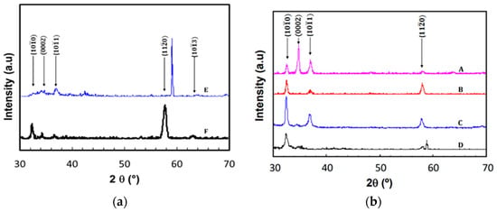
Figure 2.
X-ray diffraction patterns of GaN grown at a temperature of 680 °C with a different thickness of buffer layers. (a) GaN buffer layer: A (without buffer layer), B (16 nm), C (33 nm), and D (50 nm); (b) AlN buffer layer: E (29 nm) and F (44 nm).
We found interesting characteristics of the GaN crystal structure when the buffer layer is introduced before the growth of GaN films. As shown in Figure 2, increasing the thickness of the buffer layer from 16 nm to 33 nm still produces GaN films with crystal orientation in the , , and while the crystal orientation of (0002) is disappeared. At a buffer layer thickness of 50 nm, the crystal orientation of and still exist, while other orientations diminished. In other words, the increase in the thickness of the buffer layer causes the grown GaN films to have a crystal orientation towards the and . This growth mode is only possible if GaN templates are in the and planes. Since the template comes from crystallization of the amorphous GaN, this indicates that the crystallization GaN planes depend on the thickness of its amorphous layer. The dependence of GaN crystallites orientation on the thickness of the buffer layer was also observed by Ravash et al. [26]. The orientation of GaN crystallites is almost independent of the silicon surface direction when a thick AlN buffer layer is used. On the other hand, the crystallite orientation of GaN depends on the Si substrate orientation when a thin AlN seeding layer is applied.
Furthermore, the preferred orientation of the growth of GaN with GaN buffer layer in and plane orientation is believed to be attributed to the use of plasma nitrogen so that the growth temperature can be lowered significantly. The plasma nitrogen in our MOCVD system composes the excited states of neutral N2* molecules in the second positive system with the C3Πu → B3Πg energy level transition [21]. Compared to the N2+ ions, the excited states of the N2* molecule has lower energy, so that the growth of GaN using excited neutral molecular nitrogen (N2∗) is favorable to avoid damage to the layer grown. In addition, due to the surface formation energy of and GaN is lower than that of (0001) [27], the growth in and is the preferred orientation compared to that of (0001).
The crystal orientation of GaN films grown with the AlN buffer layer thickness of 29 nm and 44 nm is similar to that of the GaN films grown without the buffer layer, except there is an additional crystal orientation (Figure 2b). GaN films using the AlN buffer layer have more crystal orientations than the GaN films grown with the GaN buffer layer, suggesting more grain boundaries associated with the number of crystal defects in the film. Therefore, the growth of GaN films with the GaN buffer layer is preferable because the resulting GaN films have preferred crystal structure oriented in the a-axis due to the lattice mismatch between Si and GaN in the a-axis is smaller than that of Si and AlN.
Strains and dislocations caused by the lattice mismatch and the thermal expansion coefficient differences between GaN and Si(111) substrates produce structural defects. The relationship between the lattice parameters (a and c) and the Miller indices (hkl) for the hexagonal structure is used to calculate the value of the lattice parameters [28].
The strain was determined from the change of lattice constant calculated for diffraction angle of in a direction, giving a magnitude of a/ao, where ao is the lattice constant at the relaxation, which is 0.3189 nm. Figure 3 shows the lattice-constant of GaN grown with different thicknesses of buffer layer obtained from the calculation of XRD measurements. The GaN films grown with the GaN buffer layer have a smaller a-lattice constant, while the GaN grown with the AlN buffer layer has a higher lattice constant than its relaxation value. This finding is also supported by the EDS measurement, that GaN films containing a nitrogen-vacancy show a lattice shrinking.
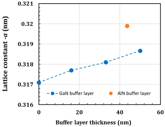
Figure 3.
The calculated lattice constants in the a-axis of the GaN films grown on Si(111) substrates as a function of GaN buffer layer thickness.
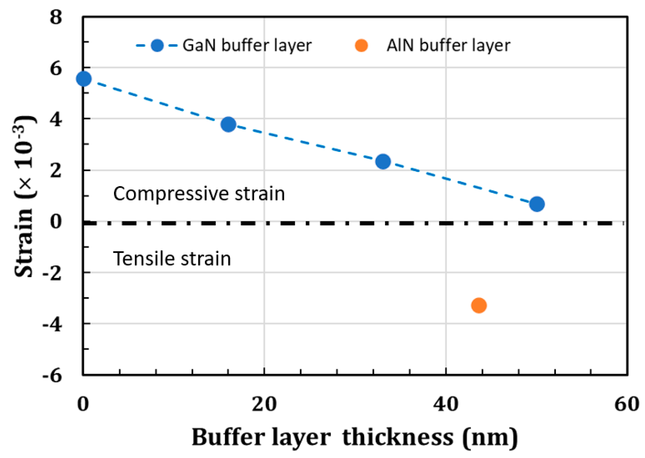
The relation between the strain and the thickness of the buffer layer is shown in Figure 4. The GaN film deposited on Si(111) substrate with or without a GaN buffer layer showed the compressive strain, while GaN grown with the AlN buffer layer showed a tensile strain. Increasing the thickness of the GaN buffer layer can reduce the strain between the Si substrate and the GaN film until it reaches film relaxation. The strain reduction is associated with the surface diffusion barrier. When the film is in tensile conditions, the surface diffusion barrier increases, while when the film is in a compressive condition, the surface diffusion barrier strain decreases [29]. The dependence of strain on the thickness of the buffer layer in our standard PA-MOCVD growth employing Si(111) as a substrate follows a pattern similar to that using the sapphire substrate to grow c-axis oriented GaN films. The difference is in the thickness of the buffer layer, which results in a relaxed GaN layer with optimum films morphology and crystal structure. The thickness of the buffer layer is higher on a sapphire substrate than on a Si(111) substrate due to a more significant lattice mismatch between c-axis GaN on sapphire and a-axis GaN on Si.

Figure 4.
The calculated strain in the a-axis of the GaN films grown on Si(111) substrates as a function of buffer layer thickness. The GaN buffer layer causes compressive strain, while the AlN buffer layer causes tensile strain.
We used EDS measurement to analyze the Ga/N atomic ratio of the grown GaN films. Table 1 shows the Ga/N atomic ratio of GaN films with GaN and AlN buffer layers. All samples have an atomic ratio of Ga/N greater than 1, suggesting the GaN films are rich in Ga atoms or nitrogen deficiency. The nitrogen deficiency is commonly found in III-nitrides grown by MOCVD, and it is caused by nitrogen vacancies, which act as native defects in GaN [30]. Based on the crystal structure, morphology, strain relaxation, and Ga/N atomic ratio, the optimum buffer layer thickness to produce high-quality GaN films is around 50 nm.
3.2. Growth of AlGaN
Using the optimized GaN buffer layer grown at 500 °C for 15 min on Si(111) substrate, AlGaN films were deposited on top of the buffer layer with various Al vapor molar fractions. AFM images of the surface morphology of AlGaN thin films grown at a ratio of V/III = 650 and a growth temperature of 700 °C are shown in Figure 5. Samples have variation in Al vapor molar fraction (xv-Al) of 20% (5a), 30% (5b), 40% (5c), and 50% (5d). The AlGaN films surface morphologies are typically homogenous, with the RMS film’s surface roughness of 2.13, 1.28, 0.74, and 0.71 nm for Al-vapor molar fraction (xv-Al) of 20%, 30%, 40%, and 50%, respectively. The smoother surface is achieved for a higher xv-Al due to the smaller grain size. The grain size of AlGaN films is related to the radius of the atoms that compose the material, which affects the size of the crystal unit cell. Because the atomic radius of Al (0.5 Å) is smaller than that of Ga (0.62 Å), increasing the Al composition on the film lowers the RMS value. Therefore, The RMS film’s surface roughness of the AlGaN film decreases as the xv-Al increases from 20% to 50%. The increase of xv-Al causes the increase of Al solid composition in AlGaN. The same reasoning applies as the film thickness decreases as the xv-Al increases or the growth rate decreases as the xv-Al flow rate increases. In general, the AlGaN surface morphology is smooth and even. We hypothesized that the smoother surface morphology is associated with the growth process, which utilizes radical nitrogen in the form of the excited-neutral molecular state of nitrogen (N2*) in the fourth positive system and the second positive system. The N2* ion has lower energy than the N+ and N2+ ions, which results in a flat film surface.

Figure 5.
A two-dimensional AFM images of AlGaN films grown at 700 °C and a ratio of V/III = 650 with different flow rates of TMAl/(TMAl + TMGa) (xv-Al), (a) 20%, (b) 30%, (c) 40%, and (d) 50%. The RMS surface roughness of AlGaN in (a–d) are 2.13, 1.28, 0.74, and 0.71 nm, respectively.
Figure 6 shows the XRD pattern of AlGaN grown with xv-Al of 10%, 20%, 30%, and 40% with a V/III ratio of 650. AlGaN with Al fraction of 10% and 20% show polycrystalline structure in the orientation and , with diffraction intensity on much higher than . As the xv-Al increases to 30% and 40%, the reflection plane vanishes, and the crystallographic structure is dominated by the plane, despite the reduced intensity. The XRD pattern shows shifting the peak from 32.42° (GaN) to 32.56°, 32.66°, 32.74°, and 32.82° as xv-Al set to 10%, 20%, 30%, and 40%, respectively. This angle shift is related to the Al solid fraction in the AlGaN film.
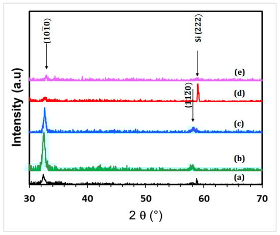
Figure 6.
X-ray diffraction patterns of AlGaN films grown at a temperature of 700 °C and a V/III ratio of 650 with various flow rate of TMAl/(TMAl+TMGa) (a) 0%, (b) 10%, (c) 20%, (d) 30%, and (e) 40%.
The AlGaN film has a polycrystalline structure that grows along the a-axis because the lattice mismatch between AlGaN and Si(111) is smaller than that along the c-axis. Therefore, the crystallographic structure formed in the a-and m-plane has the highest chance than the c-plane. The growth of AlGaN in the a-axis direction indicates that the GaN buffer layer crystallizes in the a-axis direction. The crystallization of the amorphous GaN buffer layer plays an important role in producing a template for the growth of AlGaN. The crystallization process towards the a-axis, not towards the c-axis, is probably due to the interaction between the Si(111) planes and the formation of GaN energy on the a-axis. By applying such a buffer layer, we obtain highly oriented non-polar AlGaN on Si(111).
Since the diffusion coefficients of Al and Ga are almost the same, the flow rate of the molar fraction of group III precursor theoretically determines the fraction of Al and Ga in solid-phase AlGaN by using a simple relationship between solid-phase composition and vapor phase molar fraction, which is [31]:
where FMAl and FMGa are the molar fraction of Al and Ga vapor, respectively. The molar fraction of Al in the solid phase of AlGaN can be deduced using Vegard’s law from the shifting of the peak. For xv-Al up to 40%, the stoichiometric transfer between the vapor and the solid phase occurs almost linear, as shown in Figure 7, indicating the strain has been relaxed and does not produce compositional fluctuations. No phase separation caused by inappropriate mixing of the two lattice components in the AlGaN alloy system is observed.
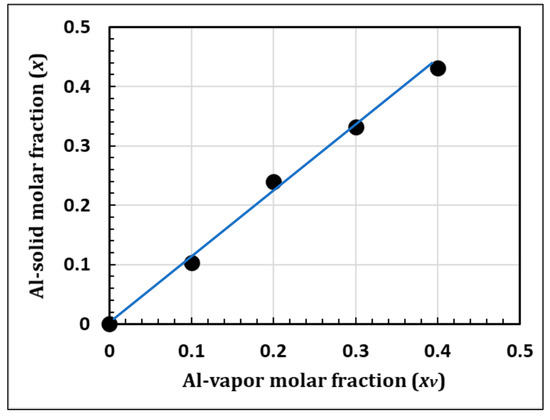
Figure 7.
The dependence of the molar fraction of Al in the solid phase on the molar fraction of Al in the vapor phase (xv-Al) of AlGaN, grown at 700 °C with a V/III ratio of 650.
4. Conclusions
We investigated the effect of GaN and AlN grown at low temperatures as a buffer layer on the growth of non-polar GaN and AlGaN. The GaN film grown without the buffer layer was polycrystal, oriented in a-and m-plane and c-plane. The morphology was rough with a separated island was formed due to a low nucleation rate. However, the morphology and crystal orientation were greatly improved by introducing GaN or AlN buffer layer. The crystallized amorphous buffer layer effectively served as a growth template. It reduced the interfacial energy between the substrate and the GaN film, allowing for a faster coalition process between islands. We correlated the effect of the buffer layer on the growth of GaN with the use of low temperature and low energy of PA-MOCVD. The morphology and crystal orientation depended significantly on the thickness of the buffer layer. We found that the GaN buffer layer was superior to AlN, and the optimum thickness of the GaN buffer layer that gave excellent morphology and crystallinity was about 50 nm. The GaN and AlGaN thin film grown on Si(111) substrate with GaN buffer layer showed a hexagonal crystallographic structure, with a preferred oriented in . The film’s surface morphology was flat and homogenous, with less than 1 nm surface roughness.
Author Contributions
Conceptualization, P.A. and H.S.; investigation, H.S., S. and A.S.; writing—original draft preparation, H.S.; writing—review and editing, P.A.; supervision, P.A.; funding acquisition, P.A. All authors have read and agreed to the published version of the manuscript.
Funding
This research was partially funded by the Integrated Research Excellent Program, Ministry of Research and Technology, The Republic of Indonesia, under contract No. 01/Perj/Dep.III/ RUT/PPKI/II.
Institutional Review Board Statement
Not applicable.
Informed Consent Statement
Not applicable.
Data Availability Statement
Not applicable.
Acknowledgments
The authors acknowledge the Directorate General for Higher Education, The Ministry of Education and Culture, The Republic of Indonesia, and Research & Community Services Council (LPPM), Institute of Technology Bandung for supporting this program.
Conflicts of Interest
The authors declare no conflict of interest.
References
- Wong, M.S.; Nakamura, S.; Denbaars, S.P. Review–Progress in High Performance III-Nitride Micro-Light-Emitting Diodes. ECS J. Solid State Sci. 2020, 9, 015012. [Google Scholar] [CrossRef]
- Wierer, J.J.; Tansu, N.; Fischer, A.J.; Tsao, J.Y. III-nitride quantum dots for ultra-efficient solid-state lighting. Laser Photonics Rev. 2016, 10, 612–622. [Google Scholar] [CrossRef]
- Mishra, U.K.; Shen, L.; Kazior, T.E.; Wu, Y.-F. GaN-Based RF Power Devices and Amplifiers. Proc. IEEE 2008, 96, 287–305. [Google Scholar] [CrossRef]
- Kukushkin, S.A.; Osipov, A.V.; Bessolov, V.N.; Medvedev, B.K.; Nevolin, V.K.; Tcarik, K.A. Substrates for epitaxy of gallium nitride: New materials and techniques. Rev. Adv. Mater. Sci. 2008, 17, 1–32. [Google Scholar]
- Kahouli, A.; Kriouche, N. Estimation of the internal electric field inside (11–22) semipolar GaN/Al0.5Ga0.5N nanostructures and the radiative efficiency at low temperature. J. Appl. Phys. 2014, 115, 193106. [Google Scholar] [CrossRef]
- Ngo, T.H.; Gil, B.; Damilano, B.; Valvin, P.; Courville, A.; de Mierry, P. Photo-induced droop in blue to red light emitting InGaN/GaN single quantum wells structures. J. Appl. Phys. 2017, 122, 063103. [Google Scholar] [CrossRef]
- Wetzel, C.; Zhu, M.; Senawiratne, J.; Detchprohm, T.; Persans, P.D.; Liu, L.; Preble, E.A.; Hanser, D. Light-emitting diode development on polar and non-polar GaN substrates. J. Cryst. Growth 2008, 310, 3987–3991. [Google Scholar] [CrossRef]
- Tanikawa, T.; Rudolph, D.; Hikosaka, T.; Honda, Y.; Yamaguchi, M.; Sawaki, N. Growth of non-polar (1120) GaN on a patterned (110)Si substrate by selective MOVPE. J. Cryst. Growth 2008, 310, 4999–5002. [Google Scholar] [CrossRef]
- Chitnis, A.; Chen, C.; Adivarahan, V.; Shatalov, M.; Kuokstis, E.; Mandavilli, V.; Yang, J.; Khan, M.A. Visible light-emitting diodes using a-plane GaN–InGaN multiple quantum wells over r-plane sapphire. Appl. Phys. Lett. 2004, 84, 3663–3665. [Google Scholar] [CrossRef]
- Craven, M.D.; Lim, S.H.; Wu, F.; Speck, J.S.; DenBaars, S.P. Structural characterization of nonpolar (1120) a-plane GaN thin films grown on (1102) r-plane sapphire. Appl. Phys. Lett. 2002, 81, 469–471. [Google Scholar] [CrossRef]
- Schulze, F.; Dadgar, A.; Bläsing, J.; Hempel, T.; Diez, A.; Christen, J.; Krost, A. Growth of single-domain GaN layers on Si(001) by metalorganic vapor-phase epitaxy. J. Cryst. Growth 2006, 289, 485–488. [Google Scholar] [CrossRef]
- Dadgar, A.; Schulze, F.; Wienecke, M.; Gadanecz, A.; Bläsing, J.; Veit, P.; Hempel, T.; Diea, A.; Christen, J.; Krost, A. Epitaxy of GaN on silicon—impact of symmetry and surface reconstruction. New J. Phys. 2007, 9, 389. [Google Scholar] [CrossRef]
- Zhu, D.; Wallis, D.J.; Humphreys, C.J. Prospects of III-nitride optoelectronics grown on Si. Rep. Prog. Phys. 2013, 76, 106501. [Google Scholar] [CrossRef] [PubMed]
- Wang, K.; Li, M.; Yang, Z.; Wu, J.; Yu, T. Stress control and dislocation reduction in the initial growth of GaN on Si (111) substrates by using a thin GaN transition layer. CrystEngComm 2019, 21, 4792–4797. [Google Scholar] [CrossRef]
- Ma, J.; Zhu, X.; Wong, K.M.; Zou, X.; Lau, K.M. Improved GaN-based LED grown on silicon (111) substrates using stress/dislocation-engineered interlayers. J. Cryt. Growth 2013, 370, 265–268. [Google Scholar] [CrossRef]
- Bolshakov, A.D.; Fedorov, V.V.; Shugurov, K.Y.; Mozharov, A.M.; Sapunov, G.A.; Shtrom, I.V.; Mukhin, M.S.; Uvarov, A.V.; Cirlin, G.E.; Mukhin, I.S. Effects of the surface preparation and buffer layer on the morphology, electronic and optical properties of the GaN nanowires on Si. Nanotechnology 2019, 30, 395602. [Google Scholar] [CrossRef]
- Uen, W.-Y.; Li, Z.-Y.; Huang, Y.-C.; Chen, M.-C.; Yang, T.-N.; Lan, S.-M.; Wu, C.-H.; Hong, H.-F.; Chi, G.-C. Heteroepitaxial growth of GaAs on Si by MOVPE using a-GaAs/a-Si double-buffer layers. J. Cryst. Growth 2006, 295, 103–107. [Google Scholar] [CrossRef]
- Remesh, N.; Chandrasekar, H.; Venugopalrao, A.; Raghavan, S.; Rangarajan, M.; Nath, D.N. Re-engineering transition layers in AlGaN/GaN HEMT on Si for high voltage applications. J. Appl. Phys. 2021, 130, 075702. [Google Scholar] [CrossRef]
- Ni, Y.; He, Z.; Yang, F.; Zhou, D.; Yao, Y.; Zhou, G.; Shen, Z.; Zhong, J.; Zhen, Y.; Wu, Z.; et al. Effect of AlN/GaN superlattice buffer on the strain state in GaN-on-Si(111) system. Jpn. J. Appl. Phys. 2014, 54, 015505. [Google Scholar] [CrossRef]
- Lin, Y.; Yang, M.; Wang, W.; Lin, Z.; Li, G. A low-temperature AlN interlayer to improve the quality of GaN epitaxial films grown on Si substrates. CrystEngComm 2016, 18, 8926–8932. [Google Scholar] [CrossRef]
- Arifin, P.; Sutanto, H.; Subagio, A.; Sugianto, S.; Mustajab, M.A. Optimization of parameters for generating nitrogen plasma in plasma-assisted MOCVD growth of InGaN thin films. AIP Adv. 2019, 9, 115304. [Google Scholar] [CrossRef]
- Weber, Z.L.; Sohn, H.; Newman, N.; Washburn, J. Electron microscopy characterization of GaN films grown by molecular-beam epitaxy on sapphire and SiC. J. Vac. Sci. Technol. B 1995, 13, 1578–1581. [Google Scholar] [CrossRef]
- Chen, P.; Xie, S.Y.; Chen, Z.Z.; Zhou, Y.G.; Shen, B.; Zhang, R.; Zheng, Y.D.; Zhu, J.M.; Wang, M.; Wu, X.S.; et al. Deposition and crystallization of amorphous GaN buffer layers on Si(111) substrates. J. Cryst. Growth 2000, 213, 27–32. [Google Scholar] [CrossRef]
- Naitoh, M.; Shimaya, H.; Watanabe, A.; Nishigaki, S. Hydrogen-induced restructuring and crater formation at Si(111) surfaces: A scanning tunneling microscopy study. Jpn. J. Appl. Phys. 1998, 37, 2033–2034. [Google Scholar] [CrossRef]
- Sawaki, N.; Hikosaka, T.; Koide, N.; Tanaka, S.; Honda, Y.; Yamaguchi, M. Growth and properties of semi-polar GaN on a patterned silicon substrate. J. Cryst. Growth 2009, 311, 2867–2874. [Google Scholar] [CrossRef]
- Ravash, R.; Blaesing, J.; Hempel, T.; Noltemeyer, M.; Dadgar, A.; Christen, J.; Krost, A. Impact of AlN seeding layer growth rate in MOVPE growth of semi-polar gallium nitride structures on high index silicon. Phys. Status Solidi B 2010, 248, 594–599. [Google Scholar] [CrossRef]
- Dreyer, C.E.; Janotti, A.; van de Walle, C.G. Absolute surface energies of polar and nonpolar planes of GaN. Phys. Rev. B 2014, 89, 081305-1–081305-4. [Google Scholar] [CrossRef]
- Suryanarayana, C.; Norton, M.G. X-Ray Diffraction: A Practical Approach; Plenum Press: New York, NY, USA, 1998; pp. 125–135. [Google Scholar]
- Lu, Y.; Liu, X.; Lu, D.-C.; Yuan, H.; Hu, G.; Wang, X.; Wang, Z.; Duan, X. The growth morphologies of GaN layer on Si(111) substrate. J. Cryst. Growth 2003, 247, 91–98. [Google Scholar] [CrossRef]
- Ganchenkova, M.G.; Nieminen, R.M. Nitrogen vacancies as major point defects in gallium nitride. Phys. Rev. Lett. 2006, 96, 196402. [Google Scholar] [CrossRef] [PubMed] [Green Version]
- DenBaars, S.P.; Keller, S. Metalorganic Chemical Vapor Deposition (MOCVD) of Group III Nitrides. In Semiconductor and Semimetal: Gallium Nitride (GaN); Pankove, J.I., Moustakas, T.D., Eds.; Academic Press: San Diego, CA, USA, 1998; Volume 50, pp. 11–35. [Google Scholar]

Publisher’s Note: MDPI stays neutral with regard to jurisdictional claims in published maps and institutional affiliations. |
© 2022 by the authors. Licensee MDPI, Basel, Switzerland. This article is an open access article distributed under the terms and conditions of the Creative Commons Attribution (CC BY) license (https://creativecommons.org/licenses/by/4.0/).