
Low-Temperature Deposition of High-Quality SiO2 Films with a Sloped Sidewall Profile for Vertical Step Coverage

 , ,
, ,
Abstract
:1. Introduction
2. Experimental
3. Results and Discussion
3.1. Influence of Process Parameters on the Step Coverage Profile
3.1.1. Effect of RF Power on the Step Coverage Profile
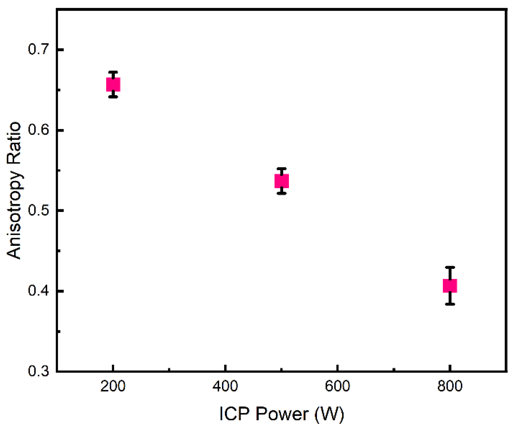
3.1.2. Effect of ICP Power on the Step Coverage Profile
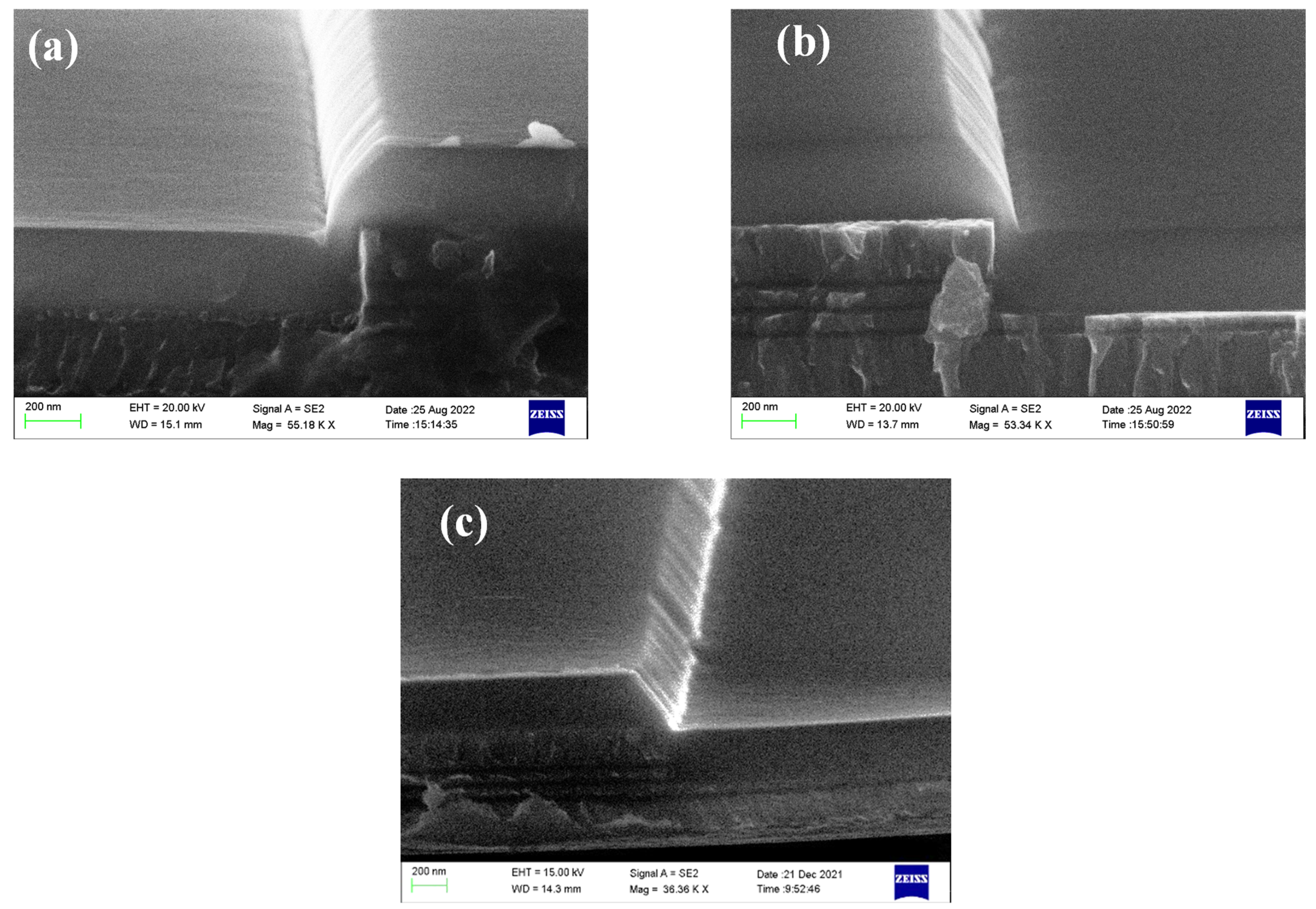
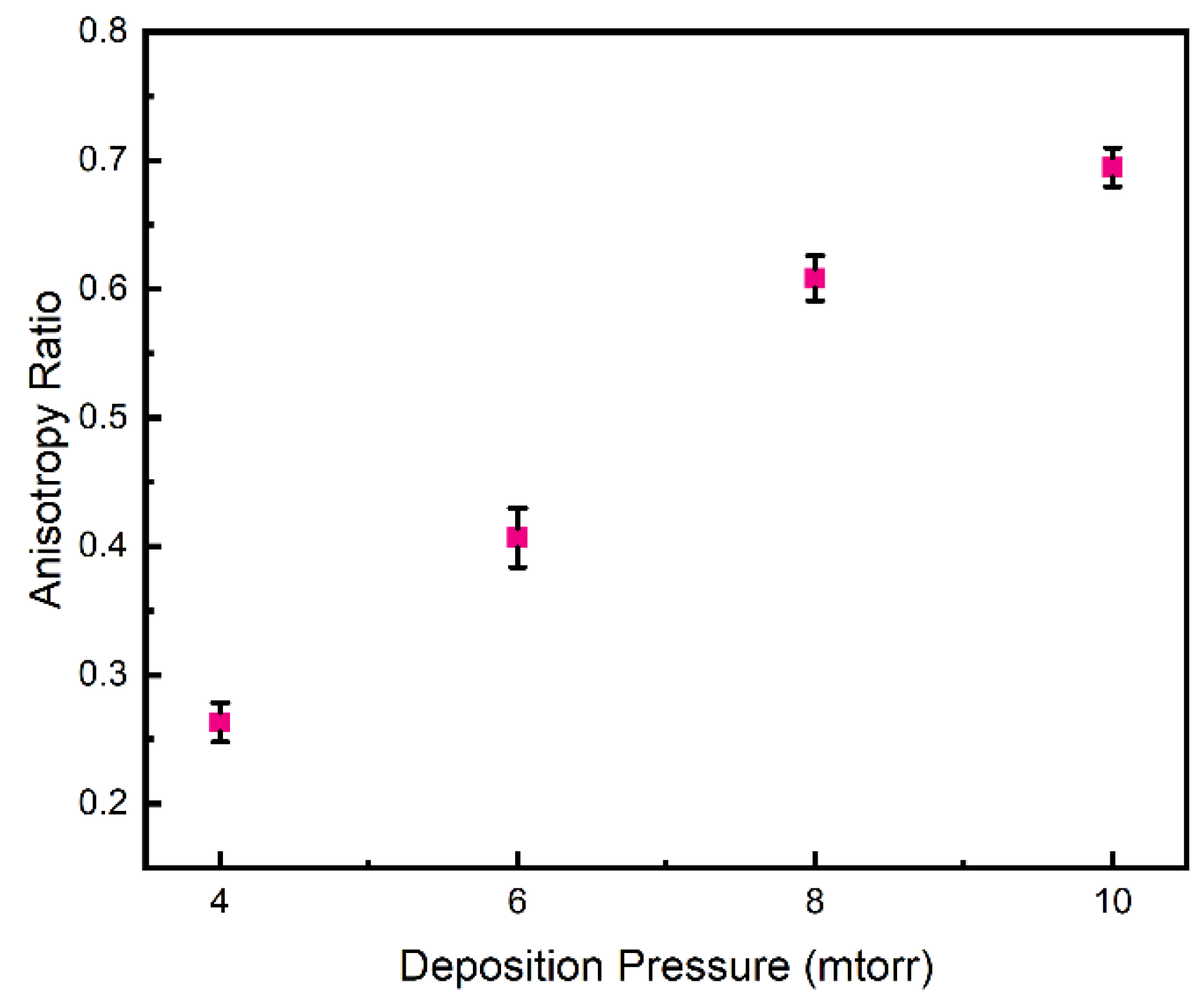
3.1.3. Effect of Deposition Pressure on the Step Coverage Profile
3.2. Film Properties
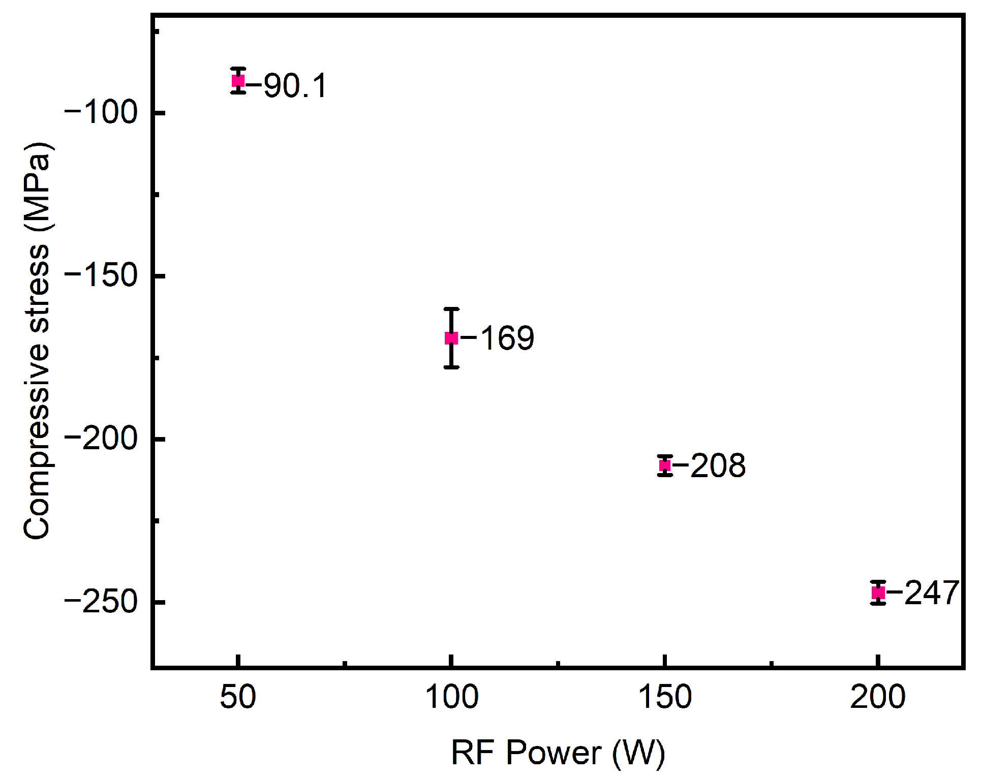
3.2.1. Film Stress
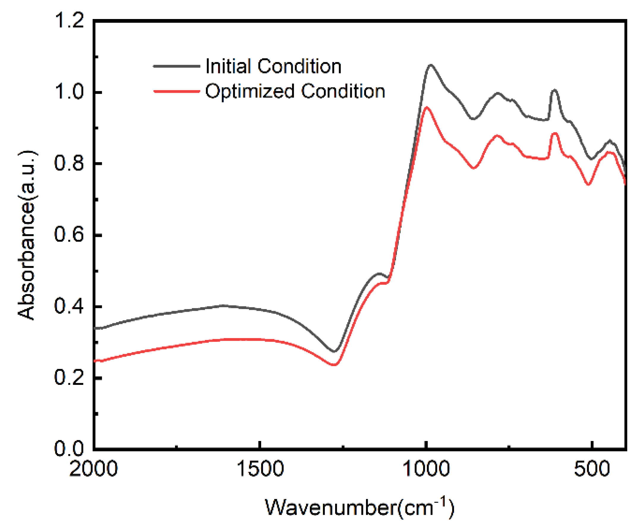
3.2.2. FTIR Spectroscopy
3.2.3. Buffered Oxide Etch (BOE) Rate
3.2.4. Roughness
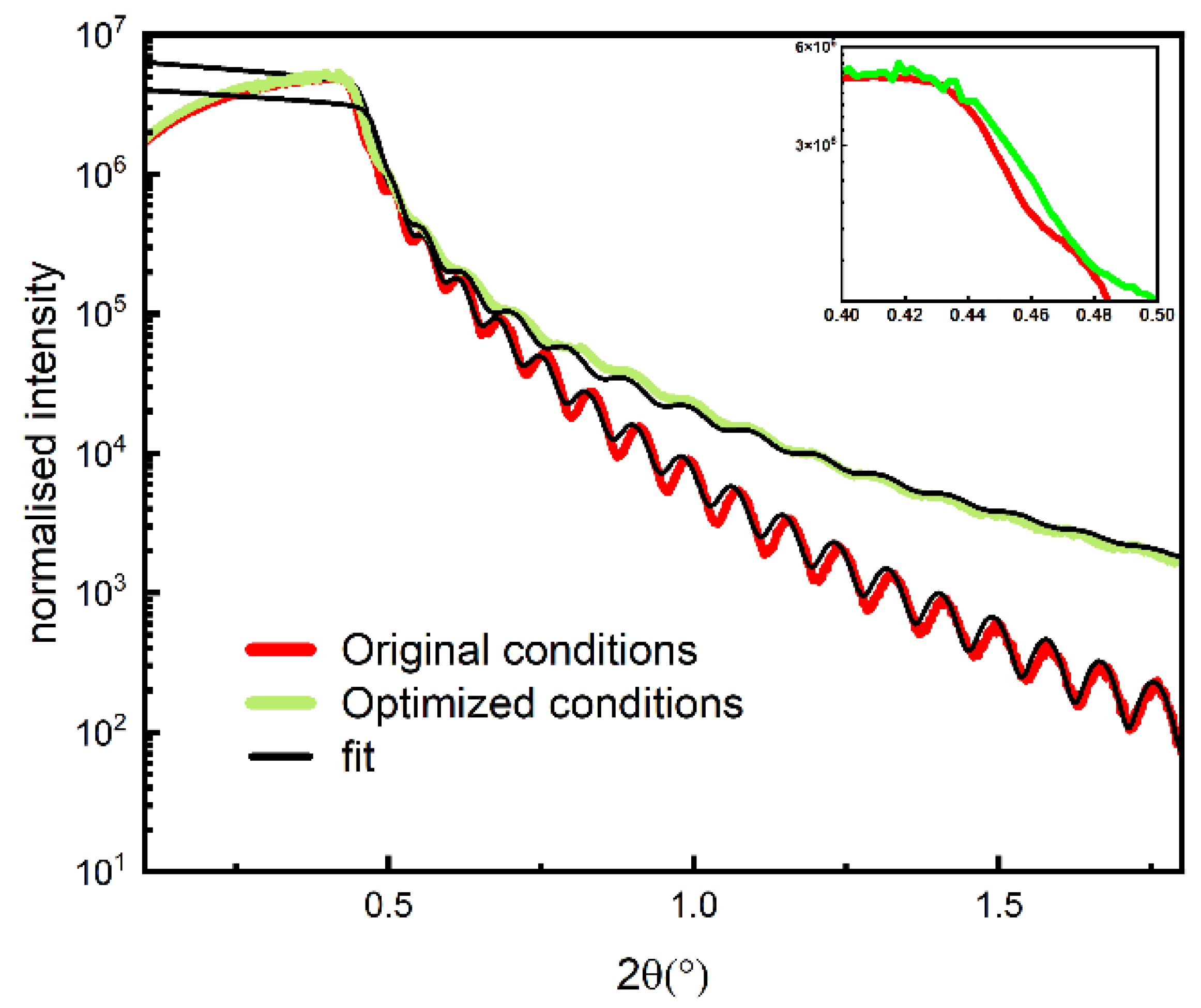
3.2.5. X-ray Reflection
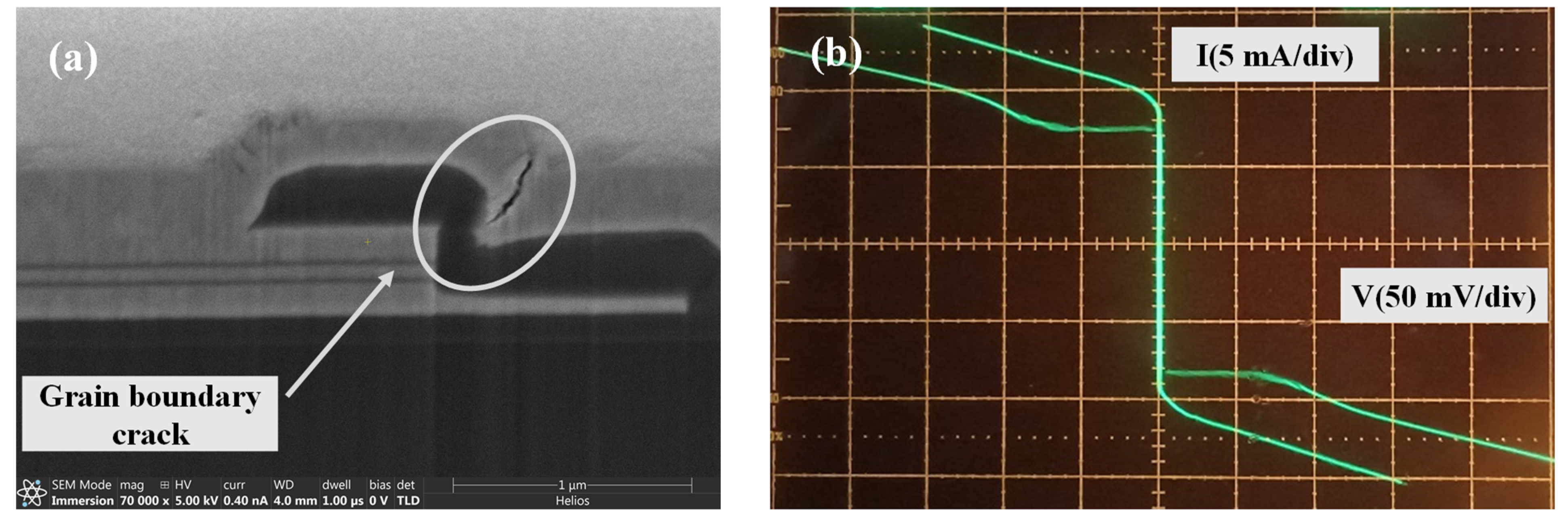
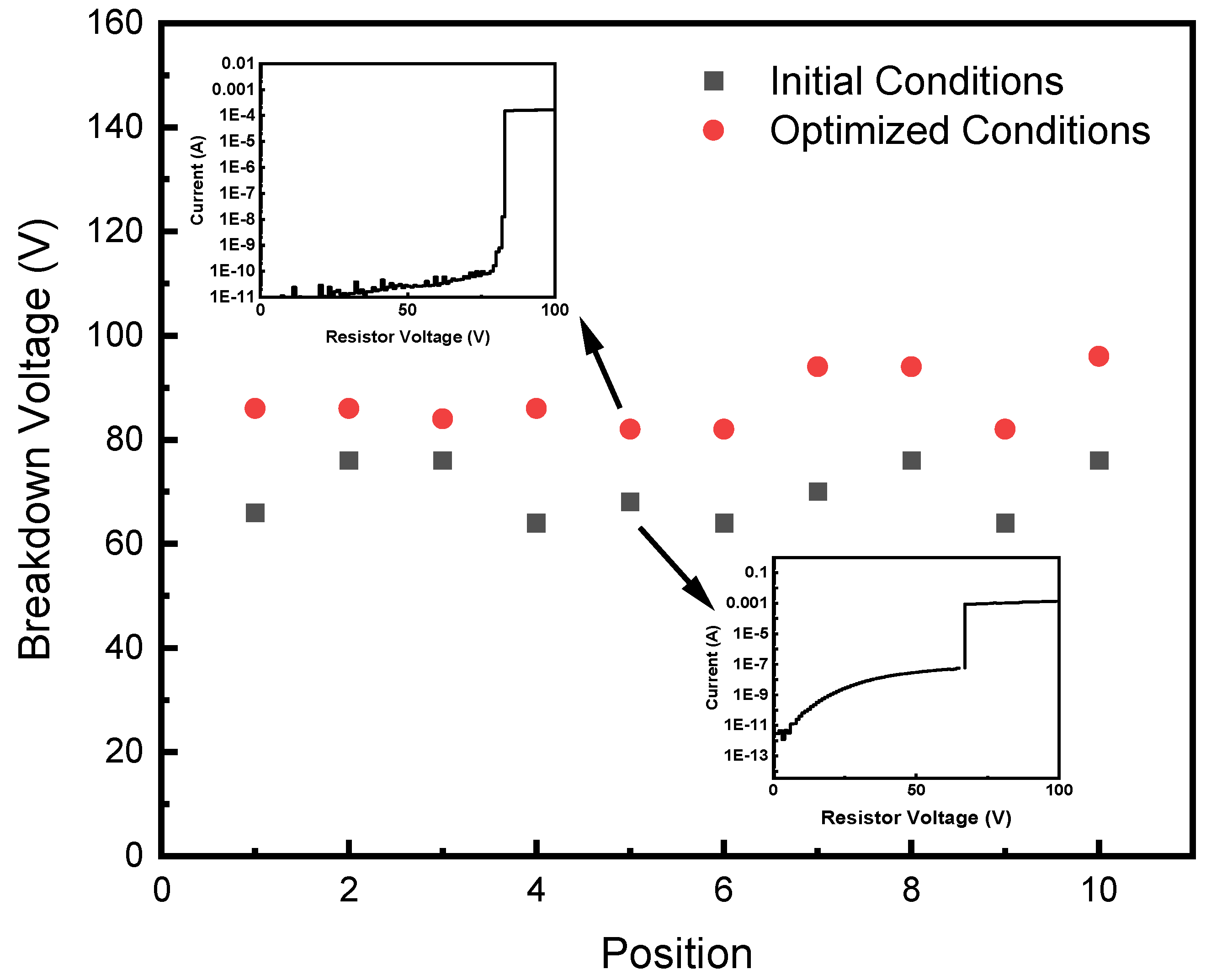
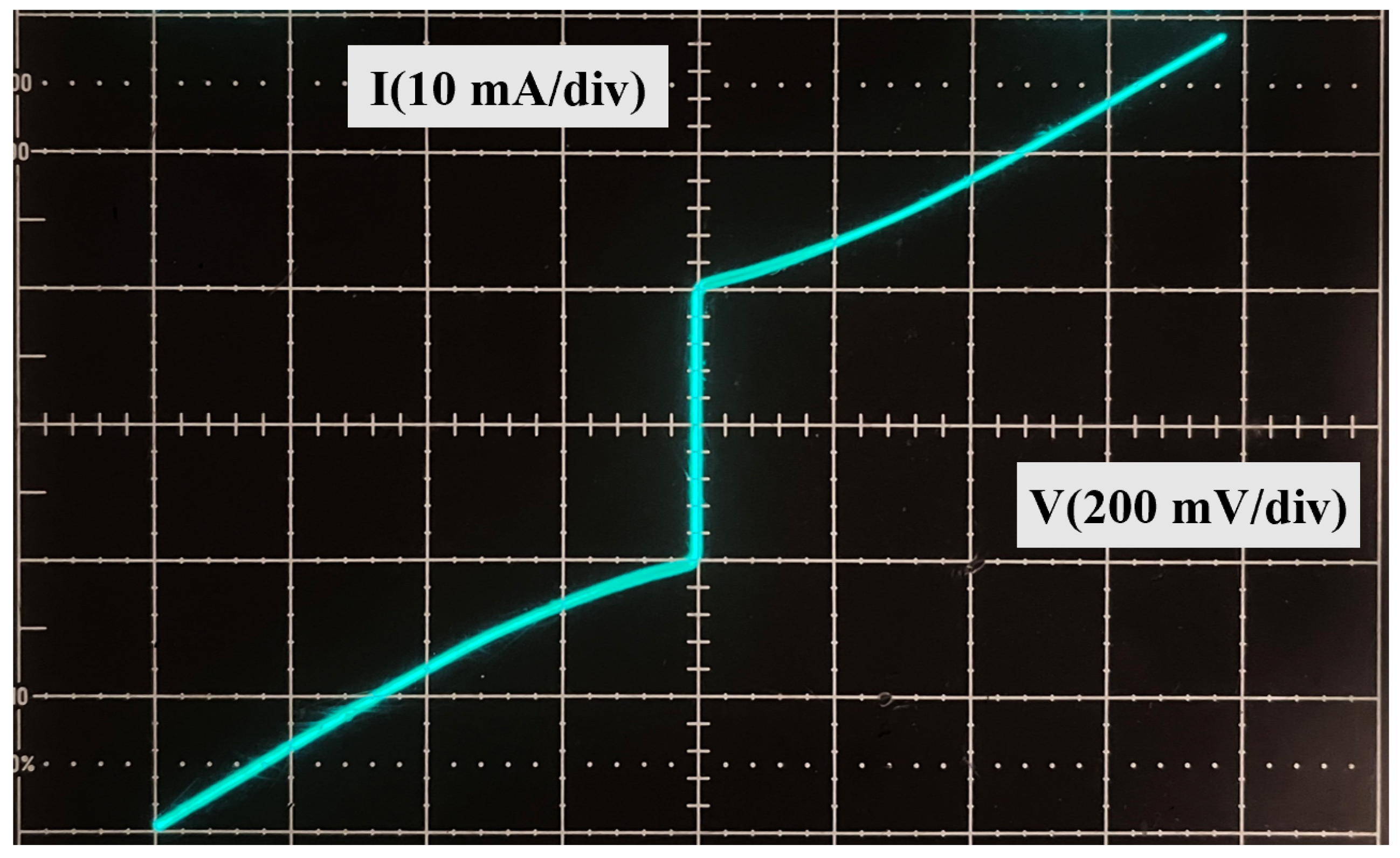
3.2.6. Breakdown Voltage
3.2.7. Application in the Device
4. Conclusions
Author Contributions
Funding
Institutional Review Board Statement
Informed Consent Statement
Data Availability Statement
Acknowledgments
Conflicts of Interest
References
- Majee, S.; Barshilia, D.; Kumar, S.; Mishra, P.; Akhtar, J. Signature of growth-deposition technique on the properties of PECVD and thermal SiO2. AIP Conf. Proc. 2017, 1998, 020023. [Google Scholar]
- Barakoa, M.T.; English, T.S.; Shilpi, R.-P.; Kennya, T.-W.; Goodson, K.-E. Dielectric barrier layers by low-temperature plasma-enhanced atomic layer deposition of silicon dioxide. Thin Solid Films 2018, 649, 24–29. [Google Scholar] [CrossRef]
- Zhu, S.; Lo, G.Q.; Kwong, D.L. Components for silicon plasmonic nanocircuits based on horizontal Cu-SiO2-Si-SiO2-Cu nanoplasmonic waveguides. Opt. Express 2012, 20, 5867–5881. [Google Scholar] [CrossRef]
- Fox, A.E.; Dresselhaus, P.D.; Rüfenacht, A.; Sanders, A.; Samuel, P.B. Junction yield analysis for 10 V programmable Josephson voltage standard devices. IEEE Trans. Appl. Superconduct. 2014, 25, 1101505. [Google Scholar] [CrossRef]
- Pan, Y.; Liu, H.; Wang, Z.; Jia, J.; Zhao, J. Optical constant and conformality analysis of SiO2 thin films deposited on linear array microstructure substrate by PECVD. Coatings 2021, 11, 510. [Google Scholar] [CrossRef]
- Nguyen, V.H.; Sekkat, A.; Masse de la Huerta, C.A.; Zoubian, F.; Crivello, C.; Rubio-Zuazo, J.; Jaffal, M.; Bonvalot, M.; Vallée, C.; Aubry, O.; et al. Atmospheric plasma-enhanced spatial chemical vapor deposition of SiO2 using trivinylmethoxysilane and oxygen plasma. Chem. Mater. 2020, 32, 5153–5161. [Google Scholar] [CrossRef]
- Baek, B.; Dresselhaus, P.D.; Benz, S.P. Thermal stability of Nb/a-NbxSi1-x/Nb Josephson junctions. Phys. Rev. B 2007, 75, 054514. [Google Scholar] [CrossRef]
- Nguyen, S.V. High-density plasma chemical vapor deposition of silicon-based dielectric films for integrated circuits. IBM J. Res. Dev. 2010, 43, 109–126. [Google Scholar] [CrossRef]
- Wostbrock, N.; Busani, T. Stress and refractive index control of SiO2 thin films for suspended waveguides. Nanomaterials 2020, 10, 2105. [Google Scholar] [CrossRef]
- Liu, J.; Liu, J.; Leng, X.; Qu, F. A Process Study of Organic/Inorganic Film Materials Deposited by ICP-PECVD at Low Temperature. Key Eng. Mater. 2017, 753, 148–155. [Google Scholar] [CrossRef]
- Jung, J.S.; Kwon, J.Y.; Park, Y.; Kim, D.Y.; Cho, H.S.; Park, K.B.; Xian, W.; Yin, H. SiO2 Film Formed by Inductivity Coupled Plasma Chemical Vapor Deposition at Low Temperature for Poly-Si TFT. J. Korean Phys. Soc. 2004, 45, 861–863. [Google Scholar]
- Chen, T.; Ryoichi, I.; Kees, B. High Quality SiO2 Deposited at 80 °C by Inductively Coupled Plasma Enhanced CVD for Flexible Display Application. Electrochem. Solid-State Lett. 2010, 13, J89–J91. [Google Scholar] [CrossRef]
- Boogaard, A.; Kovalgin, A.Y.; Brunets, I.; Aarnink, A.A.I.; Holleman, J.; Wolters, R.A.M.; Schmitz, J. Characterization of SiO2 films deposited at low temperature by means of remote ICPECVD. Surf. Coat. Technol. 2007, 201, 8976–8980. [Google Scholar] [CrossRef]
- Lien, S.Y.; Cho, Y.S.; Hsu, C.H.; Zhang, S.; Wu, W.Y.; Lien, S.Y. Mechanism of dense silicon dioxide films deposited under 100 °C via inductively coupled plasma chemical vapor deposition. Surf. Coat. Technol. 2019, 359, 247–251. [Google Scholar] [CrossRef]
- Mungekara, P.H.; Lee, S.Y. High density plasma chemical vapor deposition gap-fill mechanisms. J. Vac. Sci. Technol. 2006, 24, 11–15. [Google Scholar] [CrossRef]
- Radecker, J.; Weber, H. Extending the HDP-CVD technology to the 90 nm node and beyond with an in-situ etch assisted (ISEA) HDP-CVD process. In Proceedings of the Advanced Semiconductor Manufacturing Conference and Workshop, 2003 IEEEI/SEMI, Munich, Germany, 31 March–1 April 2003; pp. 125–130. [Google Scholar]
- Nishimura, H.; Takgi, S.; Fujino, M.; Nishi, N. Gap-Fill Process of Shallow Trench Isolation for 0.13 µm Technologies. Jpn. J. Appl. Phys. 2002, 41, 2886–2893. [Google Scholar] [CrossRef]
- Lim, M.; Papasouliotis, G.D.; Kinder, R.; Gauri, V.; Bayman, A. Gap-fill performance and film properties of PMD films for the 65 nm device technology. In Proceedings of the 2003 IEEE International Symposium on Semiconductor Manufacturing, San Jose, CA, USA, 30 September–2 October 2003; pp. 435–438. [Google Scholar]
- Huo, D.T.C.; Yan, M.F.; Chang, C.P.; Foo, P.D. Planarization of SiO2 films using reactive ion beam in plasma enhanced chemical vapor deposition. J. Appl. Phys. 1991, 69, 6637–6642. [Google Scholar] [CrossRef]
- Yota, J.; Brongo, M.R.; Dyer, T.W.; Rafftesaeth, K.P.; Bondur, J.A. Integration of ICP high-density plasma CVD with CMP and its effects on planarity for sub-0.5-um CMOS technology. In Microelectronic Device and Multilevel Interconnection Technology II; SPIE: Paris, France, 1996; Volume 2875, pp. 265–274. [Google Scholar]
- Nandakumar, M.; Sridhar, S.; Nag, S.; Mei, P.; Rogers, D.; Hanratty, M.; Amerasekera, A.; Chen, I.C. A shallow trench isolation for sub-0.13 CMOS technologies. In IEDM Technical Digest; IEEE: Piscataway, NJ, USA, 2002; pp. 657–660. [Google Scholar]
- Mannino, G.; Ruggeri, R.; Alberti, A.; Privitera, V.; Fortunato, G.; Maiolo, L. Electrical Properties of Ultrathin SiO2 Layer Deposited at 50 °C by Inductively Coupled Plasma-Enahnced Chemical Vapor Deposition. Appl. Phys. Express 2012, 5, 021103. [Google Scholar] [CrossRef]
- Revuri, P.K.; Tripathi, D.K.; Martyniuk, M.; Silva, K.K.M.B.D.; Putrino, G.; Keating, A.; Faraone, L. Silicon and Silicon dioxide thin films deposited by ICPCVD at low temperature and high rate for MEMS applications. In Proceedings of the IEEE Conference on Optoelectronic and Microelectronic Materials and Devices, Perth, Australia, 9–13 December 2018; pp. 24–26. [Google Scholar]
- Barve, S.A.; Chopade, S.S.; Kar, R.; Chand, N.; Deo, M.N.; Biswas, A.; Pate, N.N.; Rao, G.M.; Patil, D.S.; Sinha, S. SiOx containing diamond like carbon coatings: Effect of substrate bias during deposition. Diam. Relat. Mater. 2017, 71, 63–72. [Google Scholar] [CrossRef]
- Tatoulian, M. Metal edge coverage and control of charge accumulation in rf shuttered insulators. Microelectron. Reliab. 1995, 9, 182–191. [Google Scholar]
- Chang, C.P.; Pai, C.S.; Hsieh, J.I. Ion and chemical radical effects on the step coverage of plasma enhanced chemical vapor deposition tetraethylorthosilicate films. J. Appl. Phys. 1990, 64, 2119–2126. [Google Scholar] [CrossRef]
- Almeida, R.M.; Pantano, C.G. Structural investigation of silica gel films by infrared spectroscopy. J. Appl. Phys. 1990, 68, 4225–4232. [Google Scholar] [CrossRef]
- Hiramatsu, T.; Matsuda, T.; Furuta, H.; Nitta, H.; Kawaharamura, T.; Li, C.; Furuta, M.; Hirao, T. Effect of Pulsed Substrate Bias on Film Properties of SiO2 Deposited by Inductively Coupled Plasma Chemical Vapor Deposition. Jpn. J. Appl. Phys. 2014, 49, 03CA03. [Google Scholar]
- Goghero, D.; Goullet, A.; Borvon, G.; Turban, G. Effect of the ion bombardment energy on silicon dioxide films deposited from oxygen/tetraethoxysilane plasmas in a helicon reactor. Thin Solid Films 2005, 471, 123–127. [Google Scholar] [CrossRef]
- Hiroshi, F.; Mamoru, F.; Tokiyoshi, M.; Takahiro, H.; Takashi, H. SiO2 Insulator Film Synthesized at 100 °C Using Tetramethylsilane by Inductively Coupled Plasma Chemical Vapor Deposition. Jpn. J. Appl. Phys. 2007, 46, L237–L240. [Google Scholar]
- Jatta, S.; Haberle, K.; Klein, A.; Schafranek, R.; Koegel, B.; Meissner, P. Deposition of Dielectric Films with Inductively Coupled Plasma-CVD in Dependence on Pressure and Two RF-Power-Sources. Plasma Processes Polym. 2009, 6, S582–S587. [Google Scholar] [CrossRef]
- Tsai, S.Y.; Lu, Y.M.; Hon, M.H. Study on the low leakage current of an MIS structure fabricated by ICP-CVD. J. Phys. Conf. Ser. 2008, 100, 042030. [Google Scholar] [CrossRef]
- Ma, H.P.; Yang, J.H.; Yang, J.G.; Zhu, L.Y.; Huang, W.; Yuan, G.J.; Feng, J.J.; Jen, T.C.; Lu, H.L. Systematic study of the SiOx film with different stoichiometry by plasma-enhanced atomic layer deposition and its application in SiOx/SiO2 super-lattice. Nanomaterials 2019, 9, 55. [Google Scholar] [CrossRef] [Green Version]


| RF Power (W) | Bias (V) | Sputtering Etching Rate (nm/min) | Deposition Rate (nm/min) | D/S |
|---|---|---|---|---|
| 100 | 4.3 | 1.5 | 68.3 | 46.5 |
| 200 | 42 | 7.5 | 70.8 | 10.44 |
| Deposition Condition | Refractive Index | BOE Etch Rate |
|---|---|---|
| Original conditions (6 mTorr, ICP power: 800 W) | 1.4617 | 795 nm/min |
| Optimized conditions (4 mTorr, ICP power: 800 W, and RF power: 200 W) | 1.4653 | 405 nm/min |
| Thermal oxide | 1.46 | 85 nm/min |
| Deposition Condition | AVG | RMS |
|---|---|---|
| Original conditions | 0.770 | 0.618 |
| Optimized conditions | 0.162 | 0.129 |
| Deposition Condition | Thinkness | Roughness | Density |
|---|---|---|---|
| Original conditions | 96.35 | 1.3715 | 2.4771 |
| Optimized conditions | 75.72 | 0.7163 | 2.6429 |
Publisher’s Note: MDPI stays neutral with regard to jurisdictional claims in published maps and institutional affiliations. |
© 2022 by the authors. Licensee MDPI, Basel, Switzerland. This article is an open access article distributed under the terms and conditions of the Creative Commons Attribution (CC BY) license (https://creativecommons.org/licenses/by/4.0/).
Share and Cite
Liang, C.; Zhong, Y.; Zhong, Q.; Li, J.; Cao, W.; Wang, X.; Wang, S.; Xu, X.; Wang, J.; Cao, Y. Low-Temperature Deposition of High-Quality SiO2 Films with a Sloped Sidewall Profile for Vertical Step Coverage. Coatings 2022, 12, 1411. https://doi.org/10.3390/coatings12101411
Liang C, Zhong Y, Zhong Q, Li J, Cao W, Wang X, Wang S, Xu X, Wang J, Cao Y. Low-Temperature Deposition of High-Quality SiO2 Films with a Sloped Sidewall Profile for Vertical Step Coverage. Coatings. 2022; 12(10):1411. https://doi.org/10.3390/coatings12101411
Chicago/Turabian StyleLiang, Congcong, Yuan Zhong, Qing Zhong, Jinjin Li, Wenhui Cao, Xueshen Wang, Shijian Wang, Xiaolong Xu, Jian Wang, and Yue Cao. 2022. "Low-Temperature Deposition of High-Quality SiO2 Films with a Sloped Sidewall Profile for Vertical Step Coverage" Coatings 12, no. 10: 1411. https://doi.org/10.3390/coatings12101411
APA StyleLiang, C., Zhong, Y., Zhong, Q., Li, J., Cao, W., Wang, X., Wang, S., Xu, X., Wang, J., & Cao, Y. (2022). Low-Temperature Deposition of High-Quality SiO2 Films with a Sloped Sidewall Profile for Vertical Step Coverage. Coatings, 12(10), 1411. https://doi.org/10.3390/coatings12101411