
Comparative Analysis of Raman Signal Amplifying Effectiveness of Silver Nanostructures with Different Morphology

 , ,
, ,  , ,
, ,  ,
,  and
and
Abstract
:
1. Introduction
2. Materials and Methods
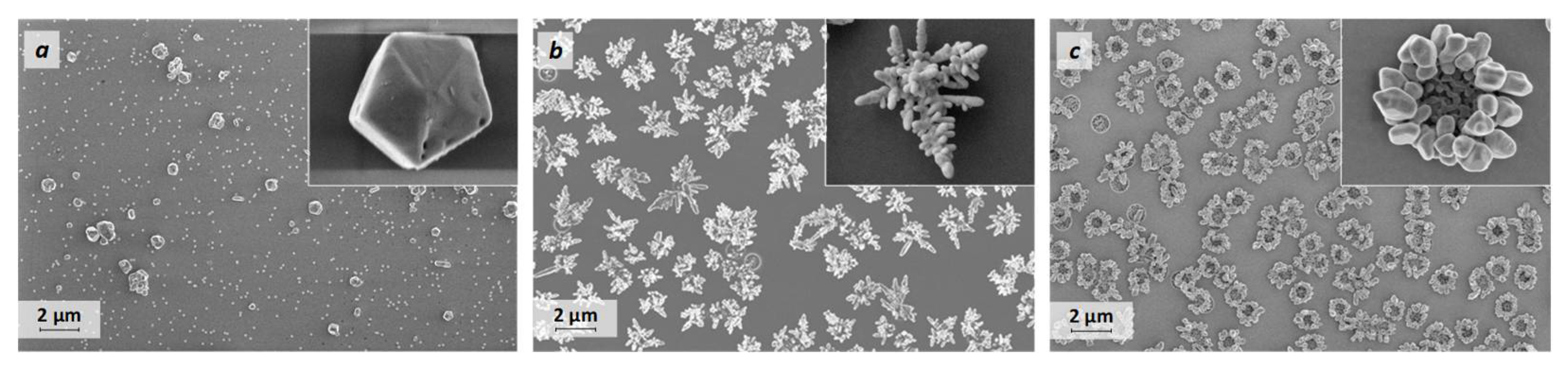
3. Results and Discussion
4. Conclusions
Author Contributions
Funding
Institutional Review Board Statement
Informed Consent Statement
Data Availability Statement
Acknowledgments
Conflicts of Interest
References
- Alula, M.T.; Mengesha, Z.T.; Mwenesongole, E. Advances in Surface-Enhanced Raman Spectroscopy for Analysis of Pharmaceuticals: A Review. Vib. Spectrosc. 2018, 98, 50–63. [Google Scholar] [CrossRef]
- Frosch, T.; Knebl, A.; Frosch, T. Recent Advances in Nano-Photonic Techniques for Pharmaceutical Drug Monitoring with Emphasis on Raman Spectroscopy. Nanophotonics 2019, 9, 19–37. [Google Scholar] [CrossRef]
- Cailletaud, J.; De Bleye, C.; Dumont, E.; Sacré, P.-Y.; Netchacovitch, L.; Gut, Y.; Boiret, M.; Ginot, Y.-M.; Hubert, P.; Ziemons, E. Critical Review of Surface-Enhanced Raman Spectroscopy Applications in the Pharmaceutical Field. J. Pharm. Biomed. Anal. 2018, 147, 458–472. [Google Scholar] [CrossRef] [PubMed]
- Adley, C. Past, Present and Future of Sensors in Food Production. Foods 2014, 3, 491–510. [Google Scholar] [CrossRef] [PubMed]
- Zheng, J.; He, L. Surface-Enhanced Raman Spectroscopy for the Chemical Analysis of Food. Compr. Rev. Food Sci. Food Saf. 2014, 13, 317–328. [Google Scholar] [CrossRef] [PubMed]
- Lin, Z.; He, L. Recent Advance in SERS Techniques for Food Safety and Quality Analysis: A Brief Review. Curr. Opin. Food Sci. 2019, 28, 82–87. [Google Scholar] [CrossRef]
- Pavel, I.; Szeghalmi, A.; Moigno, D.; Cîntă, S.; Kiefer, W. Theoretical and PH Dependent Surface Enhanced Raman Spectroscopy Study on Caffeine. Biopolymers 2003, 72, 25–37. [Google Scholar] [CrossRef] [PubMed]
- Li, D.-W.; Zhai, W.-L.; Li, Y.-T.; Long, Y.-T. Recent Progress in Surface Enhanced Raman Spectroscopy for the Detection of Environmental Pollutants. Microchim. Acta 2014, 181, 23–43. [Google Scholar] [CrossRef]
- Halvorson, R.A.; Vikesland, P.J. Surface-Enhanced Raman Spectroscopy (SERS) for Environmental Analyses. Environ. Sci. Technol. 2010, 44, 7749–7755. [Google Scholar] [CrossRef]
- Bodelón, G.; Pastoriza-Santos, I. Recent Progress in Surface-Enhanced Raman Scattering for the Detection of Chemical Contaminants in Water. Front. Chem. 2020, 8, 1–8. [Google Scholar] [CrossRef]
- Sharma, B.; Frontiera, R.R.; Henry, A.-I.; Ringe, E.; Van Duyne, R.P. SERS: Materials, Applications, and the Future. Mater. Today 2012, 15, 16–25. [Google Scholar] [CrossRef]
- Vinod, M.; Gopchandran, K.G. Au, Ag and Au:Ag Colloidal Nanoparticles Synthesized by Pulsed Laser Ablation as SERS Substrates. Prog. Nat. Sci. Mater. Int. 2014, 24, 569–578. [Google Scholar] [CrossRef]
- Cheng, M.; Fang, J.; Cao, M.; Jin, Y. Surface-Enhanced Raman Scattering Dendritic Substrates Fabricated by Deposition of Gold and Silver on Silicon. J. Nanosci. Nanotechnol. 2010, 10, 7451–7454. [Google Scholar] [CrossRef]
- Sun, X.; Lin, L.; Li, Z.; Zhang, Z.; Feng, J. Novel Ag–Cu Substrates for Surface-Enhanced Raman Scattering. Mater. Lett. 2009, 63, 2306–2308. [Google Scholar] [CrossRef]
- Kudelski, A.; Janik-Czachor, M.; Bukowska, J.; Dolata, M.; Szummer, A. Surface-Enhanced Raman Scattering (SERS) on Copper Electrodeposited under Nonequilibrium Conditions. J. Mol. Struct. 1999, 482–483, 245–248. [Google Scholar] [CrossRef]
- Wang, R.C.; Li, C.H. Cu, Cu-Cu2O Core-Shell, and Hollow Cu2O Nanodendrites: Structural Evolution and Reverse Surface-Enhanced Raman Scattering. Acta Mater. 2011, 59, 822–829. [Google Scholar] [CrossRef]
- Shao, Q.; Que, R.; Shao, M.; Cheng, L.; Lee, S.-T. Copper Nanoparticles Grafted on a Silicon Wafer and Their Excellent Surface-Enhanced Raman Scattering. Adv. Funct. Mater. 2012, 22, 2067–2070. [Google Scholar] [CrossRef]
- Kaniukov, E.; Yakimchuk, D.; Arzumanyan, G.; Terryn, H.; Baert, K.; Kozlovskiy, A.; Zdorovets, M.; Belonogov, E.; Demyanov, S. Growth Mechanisms of Spatially Separated Copper Dendrites in Pores of a SiO2 Template. Philos. Mag. 2017, 97. [Google Scholar] [CrossRef]
- Panarin, A.Y.; Terekhov, S.N.; Kholostov, K.I.; Bondarenko, V.P. SERS-Active Substrates Based on n-Type Porous Silicon. Appl. Surf. Sci. 2010, 256, 6969–6976. [Google Scholar] [CrossRef]
- Sun, B.; Jiang, X.; Dai, S.; Du, Z. Single-Crystal Silver Nanowires: Preparation and Surface-Enhanced Raman Scattering (SERS) Property. Mater. Lett. 2009, 63, 2570–2573. [Google Scholar] [CrossRef] [Green Version]
- Yakimchuk, D.; Kaniukov, E.; Bundyukova, V.; Osminkina, L.; Teichert, S.; Demyanov, S.; Sivakov, V. Silver Nanostructures Evolution in Porous SiO2/p-Si Matrices for Wide Wavelength Surface-Enhanced Raman Scattering Applications. MRS Commun. 2018, 8. [Google Scholar] [CrossRef]
- Cho, F.H.; Lin, Y.C.; Lai, Y.H. Electrochemically Fabricated Gold Dendrites with High-Index Facets for Use as Surface-Enhanced Raman-Scattering-Active Substrates. Appl. Surf. Sci. 2017, 402, 147–153. [Google Scholar] [CrossRef]
- Yakimchuk, D.V.; Bundyukova, V.D.; Ustarroz, J.; Terryn, H.; Baert, K.; Kozlovskiy, A.L.; Zdorovets, M.V.; Khubezhov, S.A.; Trukhanov, A.V.; Trukhanov, S.V.; et al. Morphology and Microstructure Evolution of Gold Nanostructures in the Limited Volume Porous Matrices. Sensors 2020, 20, 4397. [Google Scholar] [CrossRef]
- Osminkina, L.A.; Žukovskaja, O.; Agafilushkina, S.N.; Kaniukov, E.; Stranik, O.; Gonchar, K.A.; Yakimchuk, D.; Bundyukova, V.; Chermoshentsev, D.A.; Dyakov, S.A.; et al. Gold Nanoflowers Grown in a Porous Si/SiO2 Matrix: The Fabrication Process and Plasmonic Properties. Appl. Surf. Sci. 2020, 507, 144989. [Google Scholar] [CrossRef]
- Kim, S.; Jung, Y.; Gu, G.H.; Suh, J.S.; Park, S.M.; Ryu, S. Discrete Dipole Approximation Calculations of Optical Properties of Silver Nanorod Arrays in Porous Anodic Alumina. J. Phys. Chem. C 2009, 113, 16321–16328. [Google Scholar] [CrossRef]
- Ding, S.-Y.; You, E.-M.; Tian, Z.-Q.; Moskovits, M. Electromagnetic Theories of Surface-Enhanced Raman Spectroscopy. Chem. Soc. Rev. 2017, 46, 4042–4076. [Google Scholar] [CrossRef]
- Qiu, T.; Zhou, Y.; Li, J.; Zhang, W.; Lang, X.; Cui, T.; Chu, P.K. Hot Spots in Highly Raman-Enhancing Silver Nano-Dendrites. J. Phys. D. Appl. Phys. 2009, 42, 175403. [Google Scholar] [CrossRef]
- Wang, A.; Kong, X. Review of Recent Progress of Plasmonic Materials and Nano-Structures for Surface-Enhanced Raman Scattering. Materials 2015, 8, 3024–3052. [Google Scholar] [CrossRef]
- Shaw, C.P.; Fan, M.; Lane, C.; Barry, G.; Jirasek, A.I.; Brolo, A.G. Statistical Correlation between SERS Intensity and Nanoparticle Cluster Size. J. Phys. Chem. C 2013, 117, 16596–16605. [Google Scholar] [CrossRef]
- Gellner, M.; Küstner, B.; Schlücker, S. Optical Properties and SERS Efficiency of Tunable Gold/Silver Nanoshells. Vib. Spectrosc. 2009, 50, 43–47. [Google Scholar] [CrossRef]
- Willets, K.A.; Van Duyne, R.P. Localized Surface Plasmon Resonance Spectroscopy and Sensing. Annu. Rev. Phys. Chem. 2007, 58, 267–297. [Google Scholar] [CrossRef] [PubMed]
- Jones, M.R.; Osberg, K.D.; MacFarlane, R.J.; Langille, M.R.; Mirkin, C.A. Templated Techniques for the Synthesis and Assembly of Plasmonic Nanostructures. Chem. Rev. 2011, 111, 3736–3827. [Google Scholar] [CrossRef] [PubMed]
- Bamal, D.; Singh, A.; Chaudhary, G.; Kumar, M.; Singh, M.; Rani, N.; Mundlia, P.; Sehrawat, A.R. Silver Nanoparticles Biosynthesis, Characterization, Antimicrobial Activities, Applications, Cytotoxicity and Safety Issues: An Updated Review. Nanomaterials 2021, 11, 2086. [Google Scholar] [CrossRef] [PubMed]
- Pérez-Jiménez, A.I.; Lyu, D.; Lu, Z.; Liu, G.; Ren, B. Surface-Enhanced Raman Spectroscopy: Benefits, Trade-Offs and Future Developments. Chem. Sci. 2020, 11, 4563–4577. [Google Scholar] [CrossRef] [PubMed]
- Mandelbaum, Y.; Mottes, R.; Zalevsky, Z.; Zitoun, D.; Karsenty, A. Design of Surface Enhanced Raman Scattering (SERS) Nanosensor Array. Sensors 2020, 20, 5123. [Google Scholar] [CrossRef] [PubMed]
- Solís, D.M.; Taboada, J.M.; Obelleiro, F.; Liz-Marzán, L.M.; García de Abajo, F.J. Optimization of Nanoparticle-Based SERS Substrates through Large-Scale Realistic Simulations. ACS Photonics 2017, 4, 329–337. [Google Scholar] [CrossRef]
- Wei, S.; Zheng, M.; Xiang, Q.; Hu, H.; Duan, H. Optimization of the Particle Density to Maximize the SERS Enhancement Factor of Periodic Plasmonic Nanostructure Array. Opt. Express 2016, 24, 20613. [Google Scholar] [CrossRef]
- Dutta, A.; Alam, K.; Nuutinen, T.; Hulkko, E.; Karvinen, P.; Kuittinen, M.; Toppari, J.J.; Vartiainen, E.M. Influence of Fano Resonance on SERS Enhancement in Fano-Plasmonic Oligomers. Opt. Express 2019, 27, 30031. [Google Scholar] [CrossRef]
- Jeon, T.Y.; Kim, D.J.; Park, S.-G.; Kim, S.-H.; Kim, D.-H. Nanostructured Plasmonic Substrates for Use as SERS Sensors. Nano Converg. 2016, 3, 18. [Google Scholar] [CrossRef]
- Tishkevich, D.I.; Vorobjova, A.I.; Bondaruk, A.A.; Dashkevich, E.S.; Shimanovich, D.L.; Razanau, I.U.; Zubar, T.I.; Yakimchuk, D.V.; Dong, M.G.; Sayyed, M.I.; et al. The Interrelation of Synthesis Conditions and Wettability Properties of the Porous Anodic Alumina Membranes. Nanomaterials 2022, 12, 2382. [Google Scholar] [CrossRef]
- Shin, Y.; Song, J.; Kim, D.; Kang, T. Facile Preparation of Ultrasmall Void Metallic Nanogap from Self-Assembled Gold-Silica Core-Shell Nanoparticles Monolayer via Kinetic Control. Adv. Mater. 2015, 27, 4344–4350. [Google Scholar] [CrossRef]
- Jeon, T.Y.; Park, S.-G.; Lee, S.Y.; Jeon, H.C.; Yang, S.-M. Shape Control of Ag Nanostructures for Practical SERS Substrates. ACS Appl. Mater. Interfaces 2013, 5, 243–248. [Google Scholar] [CrossRef]
- Ouk Kim, S.; Solak, H.H.; Stoykovich, M.P.; Ferrier, N.J.; de Pablo, J.J.; Nealey, P.F. Epitaxial Self-Assembly of Block Copolymers on Lithographically Defined Nanopatterned Substrates. Nature 2003, 424, 411–414. [Google Scholar] [CrossRef]
- Pasquale, A.J.; Reinhard, B.M.; Dal Negro, L. Concentric Necklace Nanolenses for Optical Near-Field Focusing and Enhancement. ACS Nano 2012, 6, 4341–4348. [Google Scholar] [CrossRef]
- Ahn, S.H.; Guo, L.J. Large-Area Roll-to-Roll and Roll-to-Plate Nanoimprint Lithography: A Step toward High-Throughput Application of Continuous Nanoimprinting. ACS Nano 2009, 3, 2304–2310. [Google Scholar] [CrossRef]
- Park, S.-G.; Jeon, T.Y.; Jeon, H.C.; Kwon, J.-D.; Mun, C.; Lee, M.; Cho, B.; Kim, C.S.; Song, M.; Kim, D.-H. Fabrication of Au-Decorated 3D ZnO Nanostructures as Recyclable SERS Substrates. IEEE Sens. J. 2016, 16, 3382–3386. [Google Scholar] [CrossRef]
- Yamazoe, S.; Naya, M.; Shiota, M.; Morikawa, T.; Kubo, A.; Tani, T.; Hishiki, T.; Horiuchi, T.; Suematsu, M.; Kajimura, M. Large-Area Surface-Enhanced Raman Spectroscopy Imaging of Brain Ischemia by Gold Nanoparticles Grown on Random Nanoarrays of Transparent Boehmite. ACS Nano 2014, 8, 5622–5632. [Google Scholar] [CrossRef]
- Park, S.-G.; Mun, C.; Lee, M.; Jeon, T.Y.; Shim, H.-S.; Lee, Y.-J.; Kwon, J.-D.; Kim, C.S.; Kim, D.-H. 3D Hybrid Plasmonic Nanomaterials for Highly Efficient Optical Absorbers and Sensors. Adv. Mater. 2015, 27, 4290–4295. [Google Scholar] [CrossRef]
- Packed with Action. Adv. Mater. 2012, 24, 10–12. [CrossRef]
- Shumskaya, A.; Korolkov, I.; Rogachev, A.; Ignatovich, Z.; Kozlovskiy, A.; Zdorovets, M.; Anisovich, M.; Bashouti, M.; Shalabny, A.; Busool, R.; et al. Synthesis of Ni@Au Core-Shell Magnetic Nanotubes for Bioapplication and SERS Detection. Colloids Surfaces A Physicochem. Eng. Asp. 2021, 626, 127077. [Google Scholar] [CrossRef]
- Chu, J.; Zhao, Y.; Li, S.-H.; Li, W.-W.; Chen, X.-Y.; Huang, Y.-X.; Chen, Y.-P.; Qu, W.-G.; Yu, H.-Q.; Xu, A.-W.; et al. A Highly-Ordered and Uniform Sunflower-like Dendritic Silver Nanocomplex Array as Reproducible SERS Substrate. RSC Adv. 2015, 5, 3860–3867. [Google Scholar] [CrossRef]
- Yakimchuk, D.V.; Kaniukov, E.Y.; Lepeshov, S.; Bundyukova, V.D.; Demyanov, S.E.; Arzumanyanm, G.M.; Doroshkevich, N.V.; Mamatkulov, K.Z.; Bochmann, A.; Presselt, M.; et al. Self-Organized Spatially Separated Silver 3D Dendrites as Efficient Plasmonic Nanostructures for Surface-Enhanced Raman Spectroscopy Applications. J. Appl. Phys. 2019, 126. [Google Scholar] [CrossRef]
- Yakimchuk, D.V.; Prigodich, U.V.; Demyanov, S.E.; Ustarroz, J.; Terryn, H.; Baert, K.; Khubezhov, S.A.; Tishkevich, D.I.; Trukhanov, A.V.; Sivakov, V.; et al. Growth Mechanism Study of Silver Nanostructures in a Limited Volume. Mater. Chem. Phys. 2022, 283, 126016. [Google Scholar] [CrossRef]
- Kaniukov, E.Y.; Ustarroz, J.; Yakimchuk, D.V.; Petrova, M.; Terryn, H.; Sivakov, V.; Petrov, A.V. Tunable Nanoporous Silicon Oxide Templates by Swift Heavy Ion Tracks Technology. Nanotechnology 2016, 27. [Google Scholar] [CrossRef] [PubMed]
- Bundyukova, V.; Kaniukov, E.; Shumskaya, A.; Smirnov, A.; Kravchenko, M.; Yakimchuk, D. Ellipsometry as an Express Method for Determining the Pore Parameters of Ion-Track SiO2 Templates on a Silicon Substrate. EPJ Web Conf. 2019, 201, 01001. [Google Scholar] [CrossRef]
- Yakimchuk, D.; Bundyukova, V.; Smirnov, A.; Kaniukov, E. Express Method of Estimation of Etched Ion Track Parameters in Silicon Dioxide Template. Phys. Status Solidi 2019, 256, 1800316. [Google Scholar] [CrossRef]
- Bundyukova, V.; Yakimchuk, D.; Shumskaya, E.; Smirnov, A.; Yarmolich, M.; Kaniukov, E. Post-Processing of SiO2/Si Ion-Track Template Images for Pores Parameters Analysis. Mater. Today Proc. 2019, 7, 828–834. [Google Scholar] [CrossRef]
- Yan, M.; Xiang, Y.; Liu, L.; Chai, L.; Li, X.; Feng, T. Silver Nanocrystals with Special Shapes: Controlled Synthesis and Their Surface-Enhanced Raman Scattering Properties. RSC Adv. 2014, 4, 98–104. [Google Scholar] [CrossRef]
- Sivakov, V.; Kaniukov, E.Y.; Petrov, A.V.; Korolik, O.V.; Mazanik, A.V.; Bochmann, A.; Teichert, S.; Hidi, I.J.; Schleusener, A.; Cialla, D.; et al. Silver Nanostructures Formation in Porous Si/SiO2 Matrix. J. Cryst. Growth 2014, 400, 21–26. [Google Scholar] [CrossRef]
- Michota, A.; Bukowska, J. Surface-Enhanced Raman Scattering (SERS) of 4-Mercaptobenzoic Acid on Silver and Gold Substrates. J. Raman Spectrosc. 2003, 34, 21–25. [Google Scholar] [CrossRef]
- Song, C.; Wang, Z.; Yang, J.; Zhang, R.; Cui, Y. Preparation of 2-Mercaptobenzothiazole-Labeled Immuno-Au Aggregates for SERS-Based Immunoassay. Colloids Surf. B Biointerfaces 2010, 81, 285–288. [Google Scholar] [CrossRef]
- Rai, A.K.; Singh, R.; Singh, K.N.; Singh, V.B. FTIR, Raman Spectra and Ab Initio Calculations of 2-Mercaptobenzothiazole. Spectrochim. Acta Part A Mol. Biomol. Spectrosc. 2006, 63, 483–490. [Google Scholar] [CrossRef]
- Temple, P.A.; Hathaway, C.E. Multiphonon Raman Spectrum of Silicon. Phys. Rev. B 1973, 7, 3685–3697. [Google Scholar] [CrossRef]


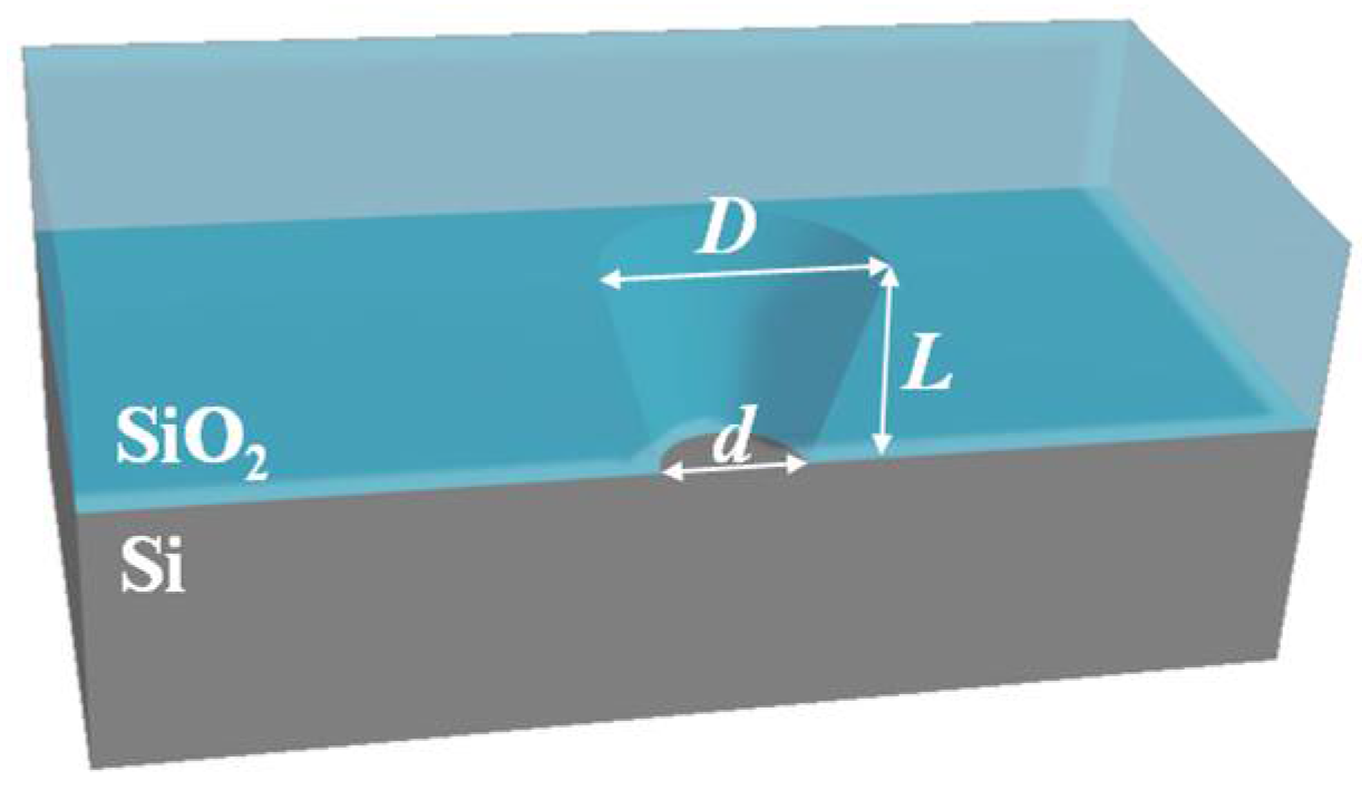
| D, nm | d, nm | L, nm |
|---|---|---|
| 320 ± 12 | 0 ± 13 | 493 ± 19 |
| 800 ± 28 | 695 ± 27 | 163 ± 7 |
| 1000 ± 35 | 980 ± 33 | 26 ± 4 |
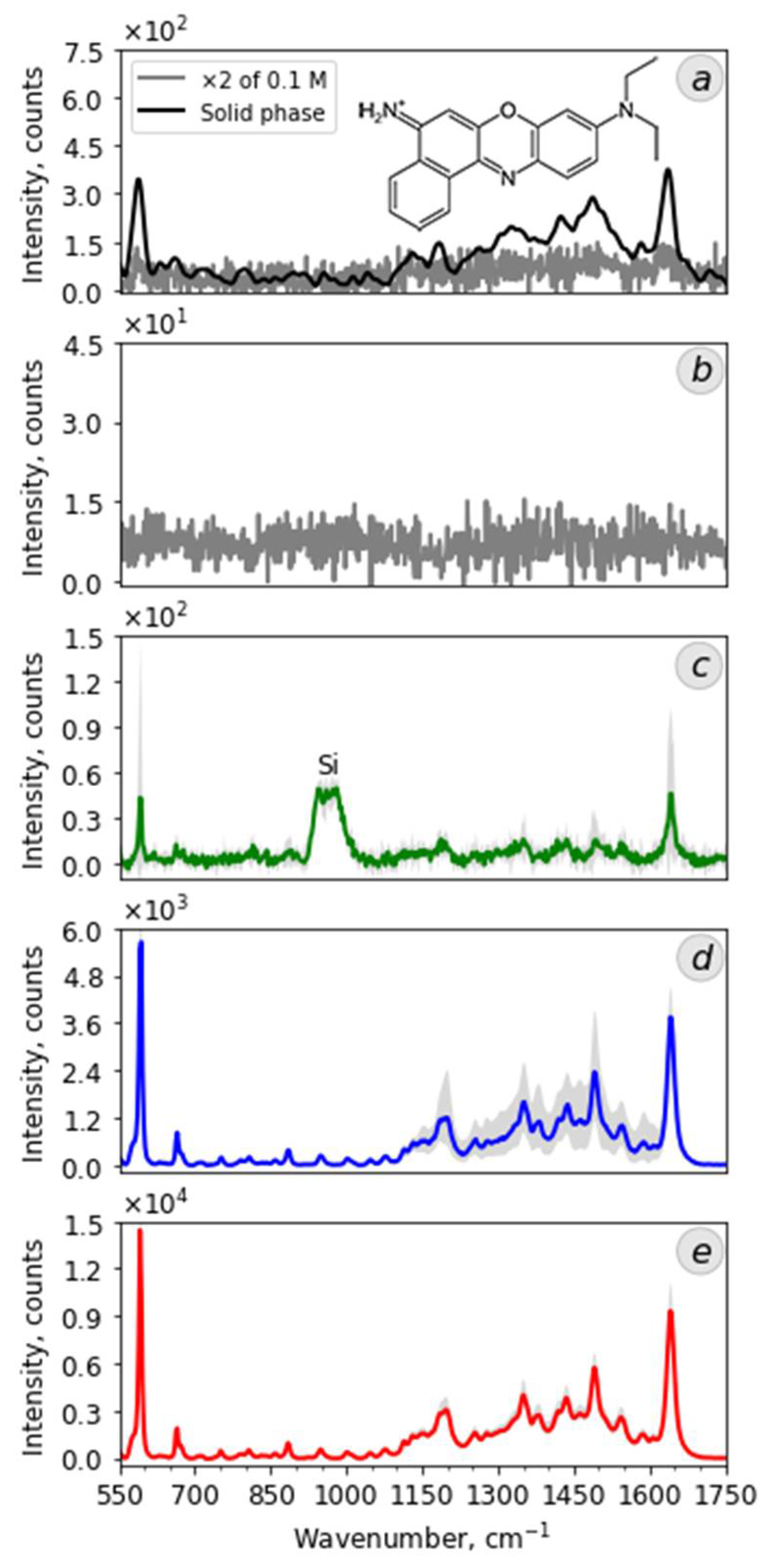
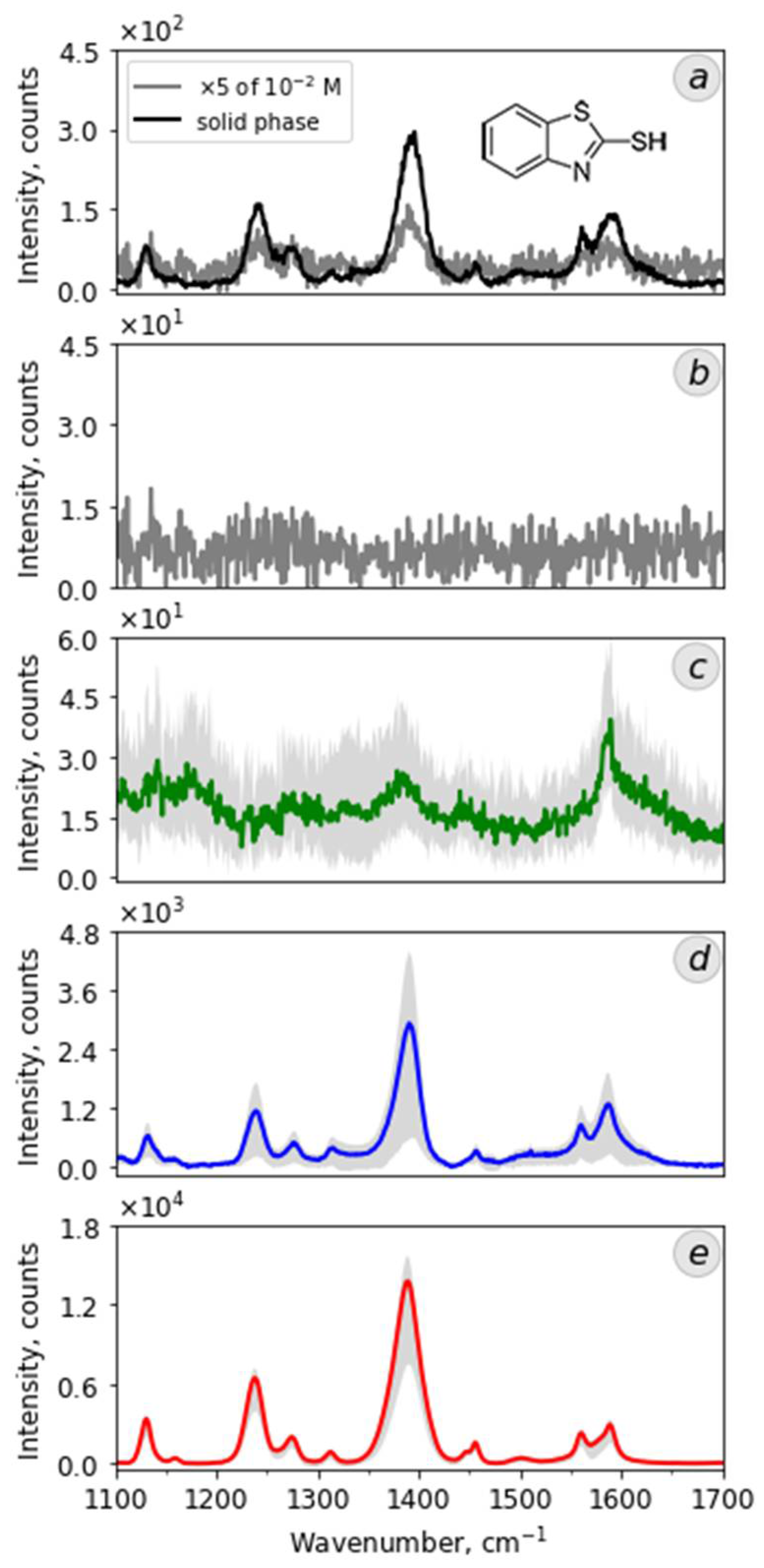
| Analyte Concentration, M | NB Line Intensity, Counts | MBT Line Intensity, Counts | ||
|---|---|---|---|---|
| 590 cm−1 | 1600 cm−1 | 1380 cm−1 | 1589 cm−1 | |
| 0.1–NB; 10−2–MBT | 345 | 375 | 31 | 19 |
| 10−6 on crystals | 43 | 46 | 39 | 27 |
| 10−6 on “sunflowers” | 5648 | 3742 | 2909 | 1261 |
| 10−6 on dendrites | 14,448 | 9329 | 13,734 | 2910 |
| Type of Silver Nanostructures | NB | MBT | ||
|---|---|---|---|---|
| EF of 590 cm−1 | EF of 1600 cm−1 | EF of 1380 cm−11 | EF of 1589 cm−1 | |
| Crystals | 1.2 × 10⁴ | 1.2 × 10⁴ | 8.7 × 10³ | 2.1 × 10⁴ |
| “Sunflowers” | 1.6 × 10⁶ | 1.0 × 10⁶ | 9.4 × 10⁵ | 6.6 × 10⁵ |
| Dendrites | 4.4 × 10⁶ | 1.5 × 10⁶ | 4.3 × 10⁶ | 1.5 × 10⁶ |
Publisher’s Note: MDPI stays neutral with regard to jurisdictional claims in published maps and institutional affiliations. |
© 2022 by the authors. Licensee MDPI, Basel, Switzerland. This article is an open access article distributed under the terms and conditions of the Creative Commons Attribution (CC BY) license (https://creativecommons.org/licenses/by/4.0/).
Share and Cite
Yakimchuk, D.V.; Khubezhov, S.A.; Prigodich, U.V.; Tishkevich, D.I.; Trukhanov, S.V.; Trukhanov, A.V.; Sivakov, V.; Kaniukov, E.Y. Comparative Analysis of Raman Signal Amplifying Effectiveness of Silver Nanostructures with Different Morphology. Coatings 2022, 12, 1419. https://doi.org/10.3390/coatings12101419
Yakimchuk DV, Khubezhov SA, Prigodich UV, Tishkevich DI, Trukhanov SV, Trukhanov AV, Sivakov V, Kaniukov EY. Comparative Analysis of Raman Signal Amplifying Effectiveness of Silver Nanostructures with Different Morphology. Coatings. 2022; 12(10):1419. https://doi.org/10.3390/coatings12101419
Chicago/Turabian StyleYakimchuk, Dzmitry V., Soslan A. Khubezhov, Uladzislau V. Prigodich, Daria I. Tishkevich, Sergei V. Trukhanov, Alex V. Trukhanov, Vladimir Sivakov, and Egor Y. Kaniukov. 2022. "Comparative Analysis of Raman Signal Amplifying Effectiveness of Silver Nanostructures with Different Morphology" Coatings 12, no. 10: 1419. https://doi.org/10.3390/coatings12101419