Abstract
The objective of this work is to study for the first time the combination of electron beam (EB) surface structuring and plasma electrolytic oxidation (PEO) with the aim of providing a multiscale topography and bioactive surface to the Ti6Al4V alloy for biomedical applications. Ca and P-containing coatings were produced via 45 s PEO treatments over multi-scale EB surface topographies. The coatings morphology and composition were characterized by a means of scanning electron microscopy (SEM) and energy dispersive X-ray spectroscopy (EDS). The effect on the previous EB topography was evaluated by means of a 3D optical profilometry and electrochemical response via potentiodynamic polarization tests. In general, the PEO process, morphology, composition and growth rate of the coatings were almost identical, irrespective of the topography treated. Minimal local differences were found in terms of morphology, and the growth rate were related to specific topographical features. Nevertheless, all the PEO-coated substrates presented essentially the same corrosion resistance. Electrochemical tests revealed a localized crevice corrosion susceptibility of all the bare EB topographies, which was successfully prevented after the PEO treatment.
1. Introduction
The long-term success of orthodontic and orthopedic metallic devices depends upon minimizing implant and host bone degradation as well as providing rapid osseointegration. Titanium and its alloys offer a low toxicity, an excellent corrosion resistance in physiological media (i.e., a low ion release rate due to the natural formation of a highly stable TiO2 layer) [1] and, in comparison to stainless steels and Co–Cr alloys (~200 GPa), an elastic modulus (E ~ 110 GPa) that is closer to that of the cortical bone (10 ÷ 40 GPa). Although Ti alloys are known for osseointegration [2], their surface morphology and chemistry can be tailored to promote further initial cellular interactions towards ultimately rapid osseointegration [3].
Mechanical and chemical surface-roughening approaches (i.e., sandblasting and chemical etching) have been shown to promote early cell-to-surface interactions such as adhesion, proliferation and the metabolic activity of osteoblastic cells [4]. Further, it has been shown that linear surface features such as microgrooves can further improve cell proliferation, differentiation and alignment [5]. This approach also provides an improved biomedical interlocking with the host bone [6,7,8,9].
Electron beam (EB) surface structuring is capable of producing linear and complex microscale topographies (i.e., hexagonal or circular) that are free from cracks, pores and impurities, with a high degree of repeatability and control [10]. EB surface structuring is based on the fast melting and solidification of the metallic surface by the action of a high-speed, high-power focused electron beam. The focused EB leads to local melting and evaporation. inducing the so-called “keyhole” effect where the high vapor pressure displaces the molten material away from the center of the beam. A fast and precise deflection of the EB causes a material transport behind the beam and a subsequent fast solidification, leading to the formation of microscale features. This technique was firstly reported by Dance et al. [11] with the name Surfi-Sculpt® for a wide range of applications. Ramskogler et al. [10] used this technology to produce 2 mm wide hexagonal structures with a multiscale topography consisting of radial canal shapes 1.3–9 µm deep and 68.6–119.7 µm wide and, depending on the beam travel direction, either a central pin up to a 305 µm height or a 452 µm deep depression. The authors showed that all the structures improved the MC3T3-E1 pre-osteoblast cells spreading area with respect to the unstructured Ti6Al4V alloy for up to 24 h. Based on the same technique, microgrooves were performed successfully in different titanium alloys to favor a contact guidance for fibroblast cells and prevent a bacterial contamination at the material’s surface [12]. Grooves with a width of 10 µm and a roughness (Ra) close to 0.2 µm showed the ability to align the fibroblast cells. An additional nano structuring provoked during the structuring reduces the bacterial adhesion in the first 48 h without using active agents.
Other surface modification approaches to improve the osseointegration of Ti implants rely on the formation of osteoconductive coatings by techniques such as plasma electrolytic oxidation (PEO), which has shown clinical success in immediate loading orthodontic procedures [13]. The PEO is an advanced high voltage anodizing technique that allows the fabrication of porous and rough ceramic coatings with the aid of short-lived plasma micro-discharges favoring the incorporation of the bioactive elements (i.e., Ca, P, Zn and Mg) [14,15,16]. Compared with traditional anodizing, PEO coatings improve the corrosion resistance and surface mechanical properties (i.e., the hardness and adhesion). Moreover, the combination of the surface topography, microstructure and composition of PEO coatings promotes early cell-to-surface interactions [17]. In the last few years, with the aim being to reduce treatment costs and minimize the impact on the mechanical properties of the substrate (i.e., fatigue), short PEO treatments (<120 s), termed flash-PEO, have been developed [18].
Henceforth, the PEO treatment of a multiscale EB-structured Ti surface would combine the composition (Ca- and P-containing), roughness (Sa ≈ 0.3–0.6 µm), porosity (pore size 0.5 up to 4 µm) and corrosion protection of the PEO coating with micro-canals (width: 10–200 µm and depth: 1–20 µm) and sub-millimeter structures (lateral and vertical dimensions between 100 and 500 µm). This combination is believed to be a powerful synergy to enhance the osteoconductive, antibacterial, corrosion resistance and biomechanical interlocking of the Ti6Al4V alloy. To the best knowledge of the authors, there is no study regarding the PEO treatment of multiscale EB structures. Specifically, it is unknown what role different structure scales might play during PEO, i.e., micro-meter and sub-millimeter scales. Therefore, the present work aims to study the PEO treatment of multiscale EB structures on Ti6Al4V, together with their electrochemical behavior in a physiological media. For this, it was decided to follow a bottom-to-top approach, treating the characteristic flat surface separately after the EB, linear EB micro-grooves and linear multiscale EB.
2. Materials and Methods
2.1. Material and Electron Beam Surface Structuring
The material selected for this investigation was the α + β alloy Ti6Al4V provided in a rectangular sheet shape with dimensions 200 × 100 × 2 mm. Prior to the EB processing, the surface contaminations were removed mechanically, generating a surface roughness (Sa) of approximately 4 μm, and the surface was subsequently cleaned with isopropanol.
The surface structuring was performed using an electron beam machine (EB) model Probeam EBG 45 ÷ 150 K14 (Probeam GmbH & Co. KGaA, Gilching, Germany), with a maximum acceleration voltage and power of 150 kV and 45 kW, respectively. The structuring of a surface is driven by the melting of the material and its displacement as the electron beam scans the surface. The melting is dependent on the energy input per the unit of length (E, [J/m]), which is ultimately dependent on the acceleration voltage (U, [V]), beam current (I, [A]) and deflection velocity (v, [m/s]): . Due to the “keyhole” effect, the molten material is displaced behind the beam and subsequently solidifies. It implies that controlling the deflection of the beam determines the accumulation of the material and, ultimately, the surface structuring.
Since electrons serve as the energy source, the negatively charged subatomic particles can be easily deflected by the magnetic lenses in the beam gun column to form geometric patterns called beam figures. These beam figures can be designed independently and implemented in the process, which then defines the trajectory of the electron beam. In the present study, the beam figures were designed using MATLAB R2017a software (MathWorks, Natick, MA, USA). In addition to the geometric dimensions (x and y coordinates), each beam figure consists of a number of coordinates/elements.
In order to proceed with the electrochemical characterization and PEO treatment, it was required that the beam figures/specimens had a square 20 × 20 mm area covered by EB structures. Henceforth, the EB structure height was fixed at 20 mm. The following EB structures/beam figures were designed to study the effect of the microstructure (i.e., martensitic α’ Ti) separately, multiple topography scales on the PEO treatment and electrochemical corrosion behavior:
The plain EB surface (designated M): molten and solidified surface with α’ martensitic microstructure, to form an identical microstructure compared to ii and iii (Figure 1).
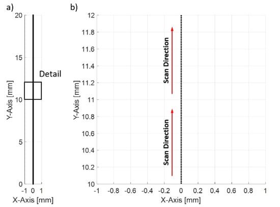
Figure 1.
(a) Electron beam scan strategy followed to produce the molten surface (M). (b) detailed view of (a).
The micro-grooves (designated G): 50 ÷ 200 μm groove/hatch spacing, 2 ÷ 15 μm deep and dimension (height × width) of 20 mm × 20 mm (Figure 2).
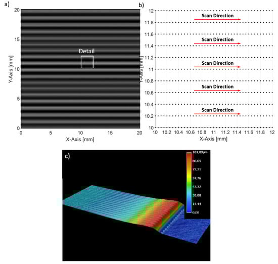
Figure 2.
(a) Electron beam scan strategy followed to produce the micro-grooves (G) over 20 mm × 20 mm area. (b) detail view of (a). (c) 3D reconstruction of beam figure.
The linear macrostructures in the center, termed “Bridge”, has perpendicular micro-grooves (designated B): 50 ÷ 200 μm groove/hatch spacing, approx. a 800 μm center height and a dimension (height × width) of 20 mm × 5 mm (Figure 3). To achieve the required dimensions (20 mm × 20 mm), four such unit cells (20 mm × 5 mm, Figure 3a) are lined up (Figure 3c).
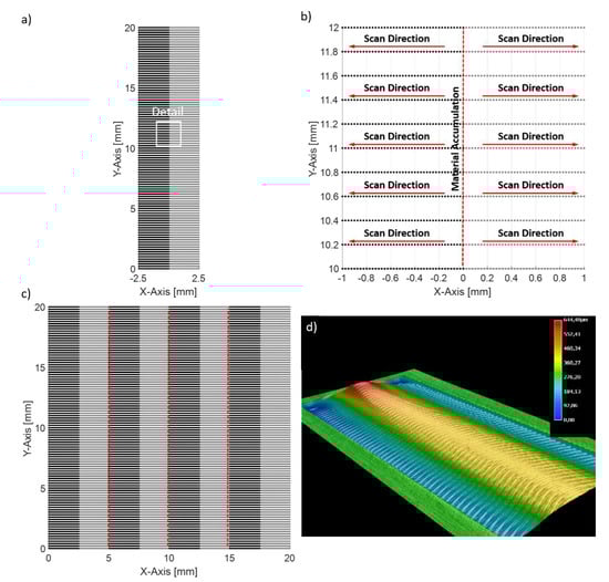
Figure 3.
(a) Electron Beam scan strategy followed to produce the bridge structures (B). (b) detail view of (a). (c) arrangement of four bridge structures covering a 20 mm × 20 mm area. (d) 3D reconstruction of the single Bridge beam figure (a).
Figure 1 shows the designed beam figure for the melting of the surface without any surface structuring. The beam figure consisted of 1000 elements, i.e., coordinates, arranged in a vertical alignment over a length of 20 mm. In contrast to the surface structuring of ii and iii, the machine table was not held stationary but moved in the x-direction at a travelling speed of 5 mm/s, while the beam figure was traversed at 1000 Hz (i.e., 1000 times per second). The required power/energy input was determined based on the preliminary studies, and for the present study, the surface was melted locally with a power input of 600 W. The parameters are summarized in Table 1.

Table 1.
Summary of input and beam oscillation parameters to achieve: M, plain EB molten and solidified surface with α’ martensitic microstructure; G1/G2, micro-grooves; B1/B2, bridge macrostructures.
Figure 2 and Figure 3 show the designed beam figures for the surface structuring to produce (i) micro-grooves and (ii) bridge linear macrostructures, respectively. For the surface structuring, the beam only was deflected, and the machine table was kept stationary. For both beam figures, the scan was line-by-line with predefined hatch spacings (i.e., vertical spacing between the beam trajectories, Figure 2b). While for the micro-grooves the beam trajectory was unidirectional from one side to the other, the beam trajectory for the linear macrostructures with perpendicular micro-grooves was multidirectional. Consequently, in addition to the micro-grooves, the multidirectional beam trajectory leads to a high linear macrostructure in the center (Figure 3d).
To determine the suitable process and beam oscillation parameters, preliminary studies were performed and the parameters varied were: (1) the beam current (0.5–2 mA), (2) hatch spacing (50–200 μm), (3) frequency (10–40 kHz) and (4) weld time, i.e., the number of passes (1–4). The final parameters were selected based on the defect-free surfaces with regular patterns and the desired feature dimensions. The selection of the specimens to be PEO treated was carried out using a digital microscope (Keyence VHX-5000, Keyence, Mechelen, Belgium), 3D analysis and scanning electron microscopy (SEM) observations (TESCAN Mira 3, Tescan, Brno, Czech Republic).
The final parameters for the further characterization of the microgrooves and linear macrostructure with perpendicular micro-grooves are listed in Table 1, respectively. A final power input of 240 W (i.e., beam current 2 mA), hatch spacing of 100 and 200 μm, frequency of 10 and 20 kHz and two passes for each beam figure were applied. The EB surface structured micro-grooves with a hatch-spacing of 100 and 200 μm are designated as G1 and G2, and the linear macrostructure with perpendicular micro-grooves with a hatch-spacing of 100 and 200 μm are designated as B1 and B2, respectively.
2.2. Flash Plasma Electrolytic Oxidation
The EB-structured samples were cleaned in ethanol in an ultrasonic bath for 5 min for both the PEO treatment and the electrochemical corrosion tests. They were subsequently attached to a copper wire as an electrical contact and electrically insulated with a commercial stopping-off resin (Lacquer 45, MacDermid plc), maintaining an unmasked 1 or 3 cm2 working area (depending on the specimen size).
The electrolyte was a Ca and P-containing aqueous solution with the following composition: 0.05 M C6H10CaO 5H2O; 0.055 M NaH2PO4 2H2O; 0.025 M NaOH; and 0.15 M Na2(EDTA) 2H2O. The PEO treatment was carried out in a double-wall electrochemical cell with agitation and maintaining the temperature of the bath at ~23 °C. An AC square voltage signal with a 490 V positive pulse and a 30 V negative pulse (VRMS = 347 V) at 300 Hz and a 50% duty cycle was used for the treatment. The initial rise of the voltage was controlled using a 60 s ramp. The current density was limited to a maximum of 300 mA·cm−2. The total treatment time was 45 s to obtain thin PEO coatings (~2 ÷ 4 μm) in agreement with the flash-PEO philosophy.
2.3. Surface Metrology and Microstructural Characterization
The surfaces of the non-treated and PEO-treated samples were studied with high-resolution 3D optical metrology (InfiniteFocusSL, Bruker, Alicona). A 3D reconstruction of the surfaces provided quantitative information on the surface features. The surface and cross-section morphology and composition of the PEO coatings were studied by SEM and energy dispersive X-ray spectroscopy (EDS, Oxford X-Max 20, Gatan, Pleasanton, CA, USA) in a JEOL JSM-6400 system at 20 kV and a working distance of 15 mm. The cross-section of the specimens was prepared following the traditional metallographic preparation. The thickness of the PEO coatings was measured from the SEM cross-section images using ImageJ software.
2.4. Electrochemical Characterization
The physiological medium selected for the present work was a modified α-MEM solution containing only inorganic compounds: 6.8 g/L NaCl; 0.2 g/L CaCl2; 0.098 g/L MgSO4; 0.4 g/L KCl; 2.2 g/L NaHCO3; and 0.122 g/L Na2HPO4 (diluted in deionized water). The pH was adjusted to 7.4 ÷ 7.6 using HCl. The electrochemical tests were carried out using a Gamry Interface 1010E Potentiostat/Galvanostat/ZRA (Gamry Instruments, Warminster, PA, USA) and an Ag/AgCl reference electrode and graphite as a counter electrode. A double-wall cell connected to a water thermostat was used to maintain the electrolyte temperature at ~37 °C during the experiments. Two specimens of each condition with a working area of ~2 cm2 were tested to ensure the repeatability. The specimens were immersed in the medium and the open circuit potential (OCP) was continuously measured for 1 h. It was followed by potentiodynamic polarization tests (PDP) in the voltage range between −0.5 V and 3.5 V, with respect to the OCP, with a scan rate of 0.5 mV/s. The electrochemical tests were set up, controlled and recorded using the Gamry Instruments Framework software (Gamry Instruments, USA). The Gamry Echem Analyst and OriginPro 8 (version 8.1) were used to analyze and plot the OCP and PDP resulting curves. The corrosion potential and current densities were obtained from the Tafel extrapolation of the cathodic branch. The corrosion rates were calculated with the following formula:
where MWTi stands for the molecular weight of Ti (47.87 g/mol), ValTi for the valence (4), dTi for the density of Ti (4.51 g/cm3) and i for the corrosion current density in mA/cm2. The polarization resistance values were obtained from the linear region of the polarization curves located within ±10 mV from the Ecorr.
3. Results and Discussion
3.1. EB Modified Surface Topography and Microstructure
Figure 4a,b show the 3D topographic images and profile analysis of the micro-grooves (G; G1 hatch spacing 100 μm, G2 hatch spacing 200 μm) and the lined up unit cells of the bridge structures (B; B1 hatch spacing 100 μm, B2 hatch spacing 200 μm), respectively. Notice that the longitudinal, transversal and vertical directions were labelled (LD, TD and VD, respectively), the LD direction being the main direction of the structures: parallel to the micro-grooves in G1 and G2; and parallel to the central line of the bridges in B1 and B2. The TD profiles taken for the G1 and G2 specimens (Figure 4a) are shown in Figure 4c. It can be seen in both cases the 100 and 200 μm spacing between the micro-grooves in agreement with the design. A peak profile was found for the G1 specimen, while it had an asymmetric wave-like shape in the G2 specimen with a total height of almost half of that of the G1 profile. According to the literature [19,20,21], the main influence on the total height of the protrusion is the beam current, i.e., an increase in the beam current directly leads to an increase in the height of the protrusion, although the scan frequency also has an influence. While Tändl and Enzinger [21] observed that a decrease in the scan frequency leads to an increase in the height, Wang et al. [19] found that such a decrease does not necessarily lead to an increase in the height and that there is a more complex relationship to the formation of protrusions; i.e., if the parameter combination is chosen such that the liquid metal reaches a certain high temperature with a low viscosity, the interaction of the surface tension and vapor pressure no longer contributes much to the formation of the protrusions. This may be the case in the present study because, although the scan frequency was lower in G2 compared with G1, the local energy input (heat input) was twice as high. As a result of the greater heat input, the molten metal downstream of the beam remained at a relatively high temperature for an extended period of time, so that it did not have a sufficient amount of time to cool and had not effectively piled up. The protrusions were wider rather than taller as the increase in the heat input resulted in a wider single bead width, which is also consistent with the literature [20]. Additionally, the lateral dimensions of the single-bead lines in G2 were larger than the spacing between the subsequent lines, thus displacing the material from the previous lines, while the G1 strategy allowed for the accumulation of the material more effectively, despite the lower input energy (Figure 4c).
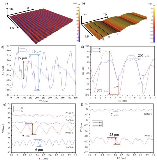
Figure 4.
(a,b): 3D reconstruction of micro-canals and bridge structures. LD: longitudinal direction along the main direction of the structures. TD: transversal direction perpendicular to the main direction of the structures. VD: vertical direction. (c): TD profiles of G1 and G2 specimens. (d): TD profiles of B1 and B2 samples. (e): LD profiles A and B of B1 and B2 samples. (f): LD profiles C of B1 and B2 samples.
The surface descriptors obtained from the 3D optical metrology of the representative areas for each structure are presented in Table 2. The G1 structure produced a rougher surface than the G2 structure, with a larger S10z in correlation with the profiles shown in Figure 4. The effective area of the G1 specimen was increased by 14%, while one of the G2 surfaces was increased by only 2.2%. The Sku parameter indicated the roundness of both surfaces (Sku < 3). On the other hand, the Ssk parameter indicated that the G1 surface had an even distribution of the peaks and valleys (Ssk near 0) while the valleys dominated the G2 surface, related to shape (Ssk < 0). It could be concluded that the G1 surface structuring was optimal in terms of the line spacing and input energy to produce a regular micro-groove topography with evenly distributed rounded peaks and valleys.
Table 2.
Surface descriptors of the bare EB structures obtained by 3D metrology. Sa: average surface roughness. Sq: square root average surface roughness. S10z: ten-point average height. Ssk: skewness parameter. Sku: kurtosis parameter. Areas analyzed: G1 and G2 4.2 mm2. B1: (5.8 × 13) 75.4 mm2. B2: (5.8 × 13) 86.54 mm2. B1-B, B1-C, B2-B and B2-C stand for the profiles B and C specified in Figure 4b,e,f. *: R10z values.
Figure 4b shows the 3D topographic image of the B2 sample. The profile plots in Figure 4d correspond to the TD profiles of both the B1 and B2 specimens. The LD profiles for both B1 and B2 along the lines indicated as A and B in Figure 4d are shown in Figure 4e. The LD profiles along line C in Figure 4e for both B1 and B2 are shown in Figure 4f. It could be seen that both B1 and B2 consisted of a central structure, i.e., a bridge, with a total height of ~220 μm and ~350 μm, respectively. The bridges were spaced by ~5 mm in agreement with the design. It is worth noticing that the structures were not symmetrical in the TD, having a sharp valley at one end of each bridge (indicated with the arrows in Figure 4d). This was due to the overlap of the bridges, i.e., a consecutive bridge removed the material from the previous one. It indicates that a further bridge width and spacing optimization would be necessary.
The LD profiles (Figure 4e,f) revealed that micro-grooves in the TD were formed while maintaining the 100 and 200 μm spacing distances. These were more regular at the sides of the bridges (the B and C profiles) than at the top (the A profiles), where the surface was irregular. It was also observed that their total height increased towards the edges of the bridge (Table 2).
The roughness parameters of the B1 and B2 samples in Table 2 correspond primarily to the bridge structures. There was an increase in the area ratio, Sa, Sq and S10z in the B2 specimen with respect to the B1 sample due to the larger amount of material which accumulated at the top part of the bridge because of the higher input energy (Table 1, Figure 4).
Considering the profiles shown in 4c (grooves) and 4e (bridge–position B), a similar height of the grooves for G2 (scan speed 500 mm/s and energy input 480 J/m), B1 (scan speed 500 mm/s, energy input 480 J/m) and B2 (scan speed 250 mm/s, energy input 960 J/m) can be observed. This confirms previous indications which showed that with a higher energy/heat input, the height of the grooves cannot be further increased. This is unlike the low heat input G1 (scan speed 1000 mm/s, energy input 240 J/m), which has a groove height twice as large. In addition to the formation of the microgrooves, there is also a macroscopic displacement of material: (1) for the grooves from one side to the other (Figure 2c), since the deflection of the beam is unidirectional, and (2) for the bridge in the center (Figure 3d), since the beam travels alternately. The amount of locally melted material can be related to the heat input, i.e., the higher the energy input, the more material which is melted and macroscopically displaced. This is of particular interest for the bridge structure, since the alternating beam travel causes the material in the centerline to be piled up from both sides. Consequently, for the higher energy input B2, a more pronounced macroscopic material displacement can be observed in the center (Figure 4d).
Figure 5 shows the SEM images of the bare EB specimens and cross-sections. Figure 5a,b shows the surface and cross-section of the M sample where a typical α’ martensitic microstructure was found within the prior β grains due to the rapid solidification that contrasts, with respect to the initial equiaxed α + β microstructure of the Ti6Al4V alloy (Figure 5c). The relief formed at the surface by the grain boundaries and α’ needles was due to the solidification in a vacuum, as described by Ferraris et al. [12]. Figure 5d,g,j,m demonstrates that the EB structuring was successful in producing reproducible micro-grooves with the hatch distance being set by the design in each case. These figures also shown that while the micro-grooves in G1 and G2 had a linear shape, these were curved in the B1 and B2 due to the different deflection and velocity of the beam. Images 5e, h, k and n show that the relief on the surface observed in image 5a was also replicated in the structured samples. Similarly, the α’ martensitic microstructure was seen in the cross-section of these samples (Figure 5f,i,l,o).
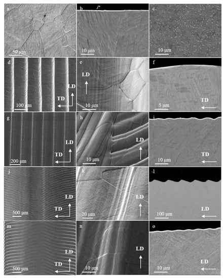
Figure 5.
Surface and cross-section SEM images of the bare EB structures: (a–c), M; (d–f), G1; (g–i), G2; (j–l), B1; and (m–o), B2. (d,g,j,m) correspond to an overview of the structures. (e,h,k,n) correspond to detail images of the EB surfaces. (f,i) TD cross-section of G1 and G2. (l,o) LD cross-section of B1 and B2 showing the cross-section of the micro-grooves.
3.2. Flash-PEO Coatings Fabrication
Figure 6 presents the RMS current density and voltage (iRMS and VRMS, respectively) during the 45 s PEO treatment for all of the specimens. The initial stage of the process (<15 s) consists of the growth of a TiO2 anodic film on the surface of the samples at a near-constant iRMS (~50 mA·cm−2) while the VRMS increases at a constant ratio. Beyond 15 s of the process, the iRMS increases rapidly up to 300 mA·cm−2 (maximum limit set). The first visible sparks accompanied the current rise on the surface of the specimens. The current surge’s initiation was the only significant difference between the molten material and the structured samples. The iRMS of the G1 specimen followed a nearly identical trend to the M sample. The current rising was delayed by ~3 s for the G2 and B1 specimens and around 5 s for the B2 surface, showing a slower rise. Nevertheless, the current density reached the maximum in all of the samples for the same treatment time, and the process continued without any other difference.
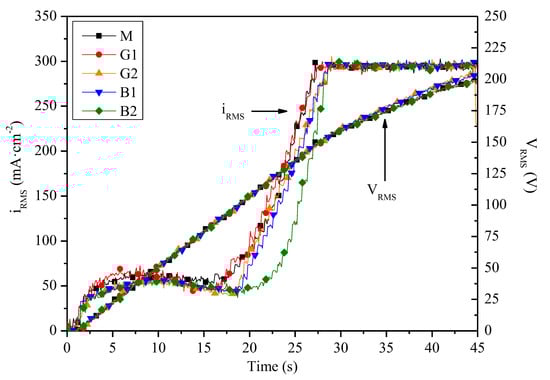
Figure 6.
Evolution of the RMS current density and voltage (iRMS and VRMS, respectively) during the PEO treatments.
3.3. Microstructural Characterization of Flash-PEO Coatings
3.3.1. Flash-PEO Coatings on Flat Molten Surface
The PEO-treated molten material (herein M-PEO) showed the characteristic of a rough and porous surface of this type of Ca- and P-containing PEO coatings (Figure 7a) and a thickness of 3.2 ± 0.8 μm [22,23]. The image analysis carried out on 3 areas (10,000 μm2 each) of the surface revealed that the M-PEO coating had a mean pore size of ~0.6 µm and a surface porosity of about 5% (Table 3). The cross-section of the coating (Figure 7b) presented a sub-micrometer inner nanoporous layer in intimate contact with the substrate (black arrow in Figure 7b) and a compact outer layer that accounted for most of the coating thickness. The porosity within the film was also found to be consisting of micro-cavities and trapped gas bubbles (white arrows in Figure 7b).
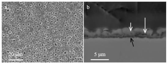
Figure 7.
(a,b): SEM of the M-PEO specimen surface and cross-section, respectively. White and black arrows indicate porosity remarks discussed in the text.
Table 3.
Porosity values obtained by image analysis for the flash-PEO coatings on the EB-structured samples. * G1-PEO-R1 and 2013R2 correspond to image analysis in regions marked in Figure 9a.
A compositional analysis of the surface (Table 4) revealed the main presence of O and Ti corresponding to the formation of TiO2. The substrate elements Al and V were also found in a small amount (<2 at.%), indicating their incorporation in the coating. The incorporation of the electrolyte-derived elements P and Ca was also confirmed, P being predominant over Ca and with a Ca to P atomic ratio of 0.7.
Table 4.
Energy dispersive X-ray spectroscopy (EDS) of PEO-treated specimens. Values given in at.%.
3.3.2. Flash-PEO of EB Surface Structures
The TD profiles obtained from the 3D topographic images of the G1-PEO and G2-PEO specimens are shown in Figure 8. It was found that the periodicity, shape and vertical and lateral sizes of the micro-grooves (Figure 4c) were not altered during the flash-PEO treatment. The surface descriptors presented in Table 5 were similar to those of the bare structured samples (Table 2). These results indicated that the flash-PEO coatings did not modify the EB structures which were produced.
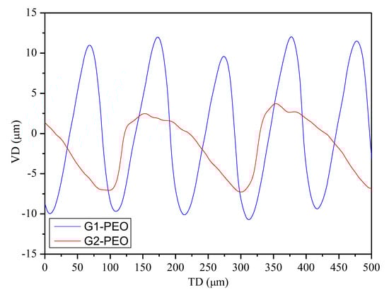
Figure 8.
TD profiles of G1-PEO and G2-PEO specimens.
Table 5.
Surface descriptors of the flash-PEO-treated specimens obtained via 3D metrology. Sa: average surface roughness. Sq: square root average surface roughness. S10z: ten-point average height. Ssk: skewness parameter. Sku: kurtosis parameter.
Flash-PEO Coatings on the Micro-Grooves Structures
The SEM images of the G1-PEO and G2-PEO coatings are shown in Figure 9. Figure 9a,c were taken over the top part of the micro-canals, which was seen as a brighter line in the image. The adjacent areas descended to the valleys of the beam figure (regions R1 and R2). Both the G1-PEO and G-PEO samples presented a comparable surface morphology to the one of the M-PEO (Figure 9b,d). Nevertheless, the surface of the G1-PEO coating seemed to have a larger number of fine pores at the bottom of the micro-canals. The image analysis carried out on the G2-PEO coating (Figure 9d) revealed porosity values similar to those of the M-PEO coating (Table 3). The image analysis of the G1-PEO was carried out over the side surfaces and (Figure 9b) valleys (regions R1 and R2 in Figure 9a). These three analyses revealed that the mean and maximum pore sizes were close to the M-PEO coating, but there were a higher pore population and a slightly higher porosity (Table 3).
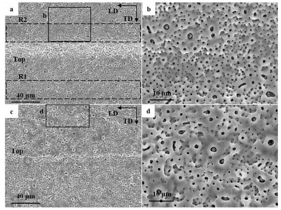
Figure 9.
SEM surface of G1-PEO (a,b) and G2-PEO (c,d) samples. Dashed regions R1 and R2 in image a mark the regions analyzed for porosity in Table 3.
The EDS area measurements (Table 4) of the G1-PEO and G2-PEO specimens show the Ca and P contents in agreement with those of the M-PEO coating. Figure 10 presents the cross-section of the G1-PEO and G2-PEO specimens, which revealed a similar morphology and thickness (Table 6) to the M-PEO coating.
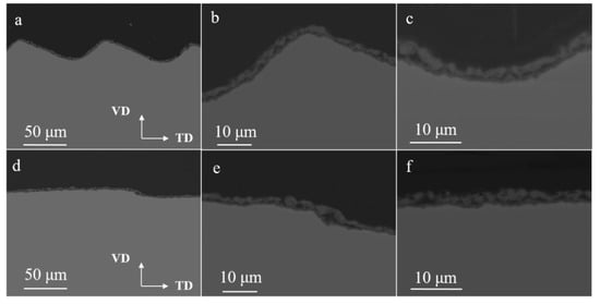
Figure 10.
Cross-section SEM of G1-PEO (a–c) and G2-PEO (d–f) coatings. Notice that cross-sections corresponded to the VD-TD plane across the micro-grooves.
To summarize, the most remarkable finding was the greater pore population of the G1-PEO. The agreement in pore size, thickness and composition between the three samples indicated a similar PEO growth rate. Henceforth, it is suggested that the higher pore density in G1-PEO was related to a greater heat diffusion during the PEO, steaming from a larger surface area, promoting a faster solidification of molten oxide and preventing finer pores from clogging [24]. On the other hand, a lower heat diffusion allowed for the flow of molten oxide in M-PEO and G2-PEO, producing a smoother surface near the larger pores.
Flash-PEO Coatings on the Bridge Structures
Figure 11 shows the SEM images of the B1-PEO (a–d) and B2-PEO (e–h) specimens. Figure 11a,b,e,f were taken where the bridges overlap. Figure 11c,g shows the top part of the bridges (profile A in Figure 4b), while d and h correspond to the areas over the micro-canals formed on these structures (approximately profile B in Figure 4b). It could be seen that the coating grew over the sharp edges and perpendicular surfaces of both structures without any apparent discontinuities, and it maintained the morphology observed for the rest of the samples (Figure 11a,b,e,f). The coating formed at the top part of the structures and over the micro-canals also showed the same morphology and no defects whatsoever. The EDS area measurements of these samples (Table 4) were taken over the bridge overlaps since it was expected that any deviations from the M-PEO were most likely to appear in this region. Nevertheless, no changes in composition were observed.
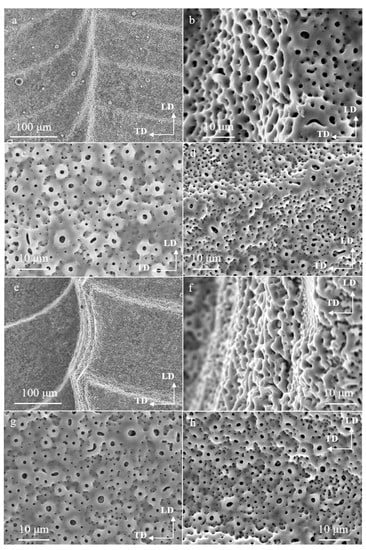
Figure 11.
SEM of B1-PEO (a–d) and B2-PEO (e–h) specimens: (a,b,e,f) were taken at the overlapping area; (c,g) at the top part of the bridges; and (d,h) at over micro-canals formed.
Figure 12 present the cross-section of the B1-PEO (a–c) and B2-PEO (d–f). Figure 12a,b,d,e corresponds to the cross-sections in the VD-TD plane at the bridges overlap. Figure 12c,f corresponds to the cross-sections in the VD-LD plane along Profile B, indicated in Figure 4, approximately. In general, the cross-section morphology of these samples was similar to that of the PEO on the molten surface. The thickness measurements revealed no significant difference with respect to the M-PEO specimen (Table 6), except at the overlap area in the B2-PEO specimen (Figure 12d,e). It is evident that the coating at the bottom of the overlap area (Figure 12e) was noticeably thinner than the coating at the adjacent region: 2.3 μm and 3.3 μm, respectively. Additionally, at the top part of the overlap, the coating thickened significantly (4.5 μm).
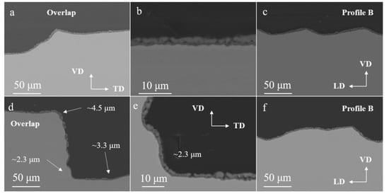
Figure 12.
Cross-section SEM of B1-PEO (a–c) and B2-PEO (d–f) coatings. Images (a,b,d,e) correspond to the VD-TD plane (across the bridge macrostructure) at the bridge overlap region. Images (c,f) correspond to the VD-LD plane across the micro-grooves of the macrostructures along the profile B (marked in Figure 4) approximately.
This suggested a lower growth rate at the bottom part of the bridge overlap, which could be linked to the delay in the current density surge of the B2-PEO specimen, as observed in Figure 6. It is believed that a lower current density passed through this region due to a poor orientation, with respect to the cathode. It may be also considered that the gas bubbles arising from the process were not easily detached, further shielding the region.
The PEO coatings at the micro-canals on the outer part of the bridge structures (Figure 12c,f, approximately the B profiles) were also similar in thickness to the coatings on the G1 and G2 structures and the molten surface, indicating that these surfaces did not produce a significant loss of efficiency during the process. Henceforth, these results suggested that beyond a 50 μm depth, careful consideration should be taken during the design of EB surface structures to avoid the electrical occlusion of the material.
3.4. Electrochemical Response
Figure 13 presents the OCP evolution during 1 h of immersion time before the potentiodynamic polarization of the non-treated and PEO-treated specimens. The non-treated samples had negative OCP values, while the PEO-treated samples showed higher values. Among the non-treated specimens, the EB-structured surfaces presented more negative OCPs.
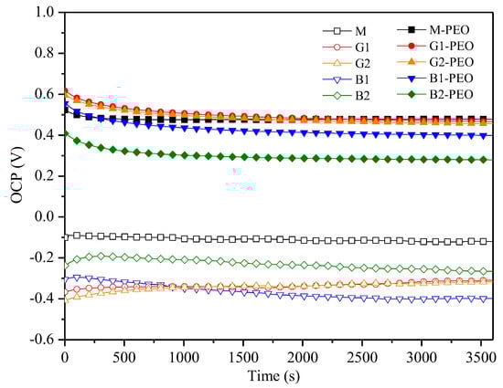
Figure 13.
Evolution of the open circuit potential (OCP) over 1 h of immersion in modified α-MEM solution.
Figure 14 presents the polarization curves of the non-treated and PEO-treated specimens. The corrosion potentials and current densities (Ecorr and icorr, respectively, obtained by Tafel extrapolation) as well as the initial potentials and currents of the passive segments (Epass and ipass) are given in Table 7. The non-treated specimens showed a negative Ecorr close to those shown during the OCP measurements, making the M specimen the noblest. The icorr was one order of magnitude higher in the structured samples, with respect to the molten surface. In turn, the corrosion rates of the bare structured specimens were found to be one order of magnitude higher (1.1–3.4 μm/year), with respect to the molten surface (0.1 μm/year). At the same time, the polarization resistance decreased one order of magnitude for the groove and bridge structures. Icorr and CR were greater and the Rp was lower for the bare bridge structures than for the groove structures, indicating a correlation with larger surface features. These effects may be assigned to defects within the natural passive oxide layer. It may be assumed that this layer was homogeneous and compact on the flat molten surface while it became more defective due to tensile stresses at the top of the convex features, such as peaks in the grooves’ specimens and the top and the sharp edges of the bridge structures. Nevertheless, it is worth recalling that all the specimens presented a passive behavior.
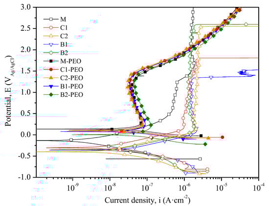
Figure 14.
Potential vs. current density (E and i, respectively) during potentiodynamic polarization experiments of bare and PEO-treated samples in modified α-MEM solution.
Table 7.
Electrochemical parameters of non-treated and PEO-treated specimens. CR stands for corrosion rate and Rp for polarization resistance. * ipass values correspond to the density current at Epass.
The molten surface presented a passive region at 4.81 × 10⁻⁷ A·cm−2 above 0.6 V. A second passivation region beyond 1.3 V at about 1.5 × 10⁻⁶ A·cm−2 was observed, which extended above 3 V. The bare structured specimens had similar passivation regions (1 ÷ 2 × 10⁻⁶ A·cm−2) above ~0.1 V. All the EB-structured samples presented a sudden increase in current density beyond 10−5 A·cm−2, which was related to localized crevice corrosion, as demonstrated by the post-mortem analysis of the tested samples.
The 3D optical topographic images of the micro-canal specimens presented in Figure 15 show that the initiation of the localized crevice corrosion started under the resin mask and spread laterally underneath it, reaching the nearby canals and advancing along the micro-canals (Figure 15a, image taken on a sample right after the initiation of the current density increase). For longer immersion times, the corrosion region spread laterally to several micro-canals at the initiation point and at the exposed surface near the resin (Figure 15b). At the same time, the corrosion advanced further along the micro-canals (Figure 15c). In the case of the bridge structures (Figure 16), crevice corrosion initiated at the overlapping areas beneath the resin. In this case, the corrosion spread laterally towards the outer parts of the bridge only at the initiation point (Figure 16a), while within the exposed area of the surface, the corrosion advanced exclusively along the overlapping area (Figure 16b). The formation of a loosely adherent light-brown gel on the surface accompanied the crevice corrosion.
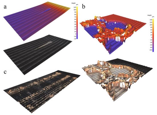
Figure 15.
Representative 3D reconstructions of localized crevice corrosion on samples G2 (a,c) and G1 (b). Image (a) shows the initiation of crevice corrosion on sample G2. Image (b) shows the corrosion pits at the initiation point of corrosion at the end of the test of sample G1. Image (c) corresponds to the whole area of G2 samples after the completion of the PDP tests.
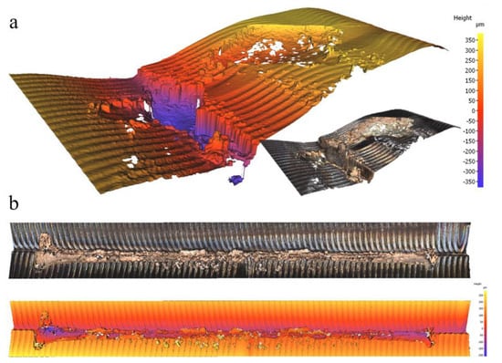
Figure 16.
Representative 3D reconstructions of localized crevice corrosion on sample B2 after the PDP test: (a) initiation point; and (b) whole surface.
The crevice corrosion takes place within the restricted volumes where oxidizing species, such as dissolved O2, are consumed faster than what is replenished from the bulk solution, preventing the formation of new oxide. This situation also involves low pH levels with the hydrolysis of titanium chlorides that form hydrochloric acid and Ti hydroxides (Ti(OH)x(4−x)), among other products [25,26,27], and the generation of an electrochemical microcell between the crevice becomes the anode and the outer exposed surface becomes the cathode.
Such a localized corrosion has been reported previously in the literature which dealt with the electrochemical behavior of the DMLS Ti6Al4V pins, where the crevice corrosion appeared at the superficial porosity and imperfections [25]. The Ti6Al4V alloys manufactured by laser-based powder bed fusion are characterized by an α’/α martensitic microstructure similar to the one formed in EB structures. Additionally, the formation of a light-brown gel was also reported and assigned to TiO2·H2O and TiO3·H2O, which presents a higher solubility and a worse adherence than TiO2. The remnants of these oxides were observed to be adhered to the specimens shown in Figure 15 and Figure 16. It might be hypothesized that such products and oxides formed within the crevice extended outside the crevice and along the micro-canals and overlapping area, occluding these valleys and leading to under deposit corrosion.
Additional PDP tests were carried out on M specimens at the pH values of 7.5, 3.6 and 2 (Figure 17). Localized corrosion, or any other type of corrosion whatsoever, was not observed in these specimens. This indicates that the consumption of the oxidizing species (i.e., dissolved O2) within the restricted volume played a more dominant role in the localized crevice corrosion of EB-treated specimens than low pH levels.
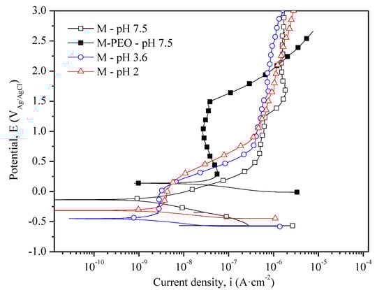
Figure 17.
Potential vs. current density (E and i, respectively) during potentiodynamic polarization experiments of bare molten surface at pH 7.5, 3.6 and 2. PDP curve of M-PEO at pH 7.5 is also given for comparison.
Finally, a crevice appeared between 1 and 2 V for the G1 and B1 specimens and between 2.5 and 3 V for the G2 and B2 samples, indicating a correlation between the crevice potential and the hatch spacing. It is believed that is related to a greater number of possible crevice locations in G1 and B1, hence increasing the chances for localized corrosion.
All the PEO-treated specimens presented an identical electrochemical behavior with positive Ecorr (~0.1 V) values, slightly lower than those of the OCP recorded. This shift is commonly observed for titanium and is related to the charging process of the electrode/solution interface capacitance. Despite the relatively slow scan rate used in this study (0.5 mV/s), which is a well-known strategy for minimizing this artefact [28], PEO-treated specimens, unlike bare substrates, showed a sufficiently high charging current to shift the Ecorr to significantly lower values than the OCP. The icorr values were found in the range between 2.5 and 4.5 × 10⁻⁸ A·cm−2, which are in agreement with the values reported for the PEO coatings on the AM Ti6A4V alloys in the biological media [29]. The icorr of the PEO-treated specimens was one order of magnitude higher than that of the bare molten surface and of the same order in comparison to the groove and bridge structures. This can be assigned to the microstructure of the inner barrier-like layer of the PEO coatings that is in intimate contact with the substrate. Such a layer is known to contain nano-pores that might explain the higher icorr and CR and lower Rp with respect to the molten surface. Nevertheless, these specimens presented a strong passive behavior and passive current densities lower than those of the un-treated specimens. All the samples reached a passive region at about 0.25 V (Epass) and a passive current (ipass) of ~8.83 × 10⁻⁸ A·cm−2. Up to 1.3 V, the current density decreased to 3.18 × 10⁻⁸ A·cm−2. Finally, the current density of the PEO-treated specimens increased rapidly beyond 1.5 V due to the oxygen evolution.
As a concluding remark, unlike the untreated structured surfaces, the PEO-treated samples did not reveal any sign of crevice corrosion. It would therefore be recommended that EB-structured Ti surfaces were treated via PEO to avoid this issue while enhancing the osteoconductivity of the surface.
4. Conclusions
The PEO treatment of EB surface structures was carried out successfully with only minimal differences at the onset of sparking. The coating morphology, thickness, composition and electrochemical properties were identical for all of the coatings. At the same time the EB structures were unchanged by the PEO process. The following remarks were drawn as the conclusions from this study:
- +
- The coating could reproduce the topography carried out with the EB process. The submicrometer topographical features were only affected by the flash process.
- +
- The PEO coatings provided a surface with a sub-micrometric roughness and a maximum thickness of ~3 µm, containing biocompatible elements in the composition (Ca/P atomic ratio of 0.8). The pore density was estimated to contain about 150 ÷ 240 pores/1000 μm2 and with a pore mean size of ~0.7 μm.
- +
- For the groove structures, a higher pore density of the fine pores was found at the bottom of the valleys in the G1 EB structure which was assigned to a higher cooling rate of the topography, leading to a faster solidification of the molten oxide, preventing the clogging of the pores.
- +
- For the bridge structures, structures with a hatch-spacing of 200 µm (B2) lead to a slightly less efficient process, delaying the onset of sparking by about 5 s. The only morphological difference was found at the bottom of the overlapping areas where the coating was thinner.
- +
- The topography of the PEO-coating did not incur in any significant differences in the electrochemical behavior, showing a passive behavior with passive current densities at approximately 9 × 10⁻⁸ A/cm−2.
- +
- The PEO-coatings prevented, effectively, the crevice corrosion in the structured surfaces. In future, it is recommended that titanium implants in contact with other surfaces or with a designed topography are subjected to PEO treatments to prevent a localized crevice corrosion.
- +
- From the point of view of the EB structuring design and fabrication, the results on this work showed that deep topographies might hinder the PEO efficiency and growth, compromising the functionality and electrochemical performance of the coating.
The combination of both techniques may be of great interest for orthodontic and orthopedic applications. For that, further investigations may need to address, to improve the functionalization of the surface, (a) the bonding strength between the PEO-treated EB surface structures and the bone, (b) a higher Ca/P ratio closer to the hydroxyapatite keeping the topography of the substrate and (c) the application of PEO treatments to finer EB structures.
Author Contributions
Conceptualization, H.M.-S., F.P., R.B., E.M. and F.W.; methodology, H.M.-S., F.P., R.B., E.M. and F.W.; formal analysis, H.M.-S., F.P., E.M. and F.W.; investigation, H.M.-S., F.P., R.B., E.M. and F.W.; resources, H.M.-S., F.P., R.B., E.M. and F.W.; writing—original draft preparation, H.M.-S., F.P. and R.B.; writing—review and editing, R.A., M.M., E.M. and F.W.; supervision, E.M. and F.W.; funding acquisition, H.M.-S., M.M., E.M. and F.W. All authors have read and agreed to the published version of the manuscript.
Funding
The authors gratefully acknowledge the support of PID2021-124341OB-C22 (MICINN/AEI/FEDER, UE) and ADITIMAT-CM (S2018/NMT-4411, the Regional Government of Madrid and EU Structural Funds). M.M. is grateful for the support of RYC-2017-21843. H.M.-S. is grateful for the support of PEJD-2019-POST/IND-16119 (the Regional Government of Madrid and EU Structural Funds), FEI-EU-20-05 (UCM) and KMM-VIN for the research fellowship (https://www.kmm-vin.eu/fellowships/) granted to carry out a research stay at the IMAT Institute (TU-Graz, Graz, Austria). R.H.B. acknowledges the Christian Doppler Forschungsgesellschaft; project number: D-1303000107.
Institutional Review Board Statement
Not applicable.
Informed Consent Statement
Not applicable.
Data Availability Statement
Not applicable.
Conflicts of Interest
The authors declare no conflict of interest.
References
- Yan Guo, C.; Tin Hong Tang, A.; Pekka Matinlinna, J. Insights into surface treatment methods of titanium dental implants. J. Adhes. Sci. Technol. 2012, 26, 189–205. [Google Scholar] [CrossRef]
- Guo, C.Y.; Matinlinna, J.P.; Tang, A.T.H. Effects of surface charges on dental implants: Past, present, and future. Int. J. Biomater. 2012, 2012, 381535. [Google Scholar] [CrossRef] [PubMed]
- Amaral, I.; Cordeiro, A.; Sampaio, P.; Barbosa, M. Attachment, spreading and short-term proliferation of human osteoblastic cells cultured on chitosan films with different degrees of acetylation. J. Biomater. Sci. Polym. Ed. 2007, 18, 469–485. [Google Scholar] [CrossRef] [PubMed]
- Nishimura, N.; Kawai, T. Effect of microstructure of titanium surface on the behaviour of osteogenic cell line MC3T3-E1. J. Mater. Sci. Mater. Med. 1998, 9, 99–102. [Google Scholar] [CrossRef]
- Fu, J.; Hu, Y.; Guo, Z.; Zhang, Y.; Hao, Y.; Li, S. Effect of surface micro-topography of titanium material on the behaviors of rabbit osteoblast in vitro. Appl. Surf. Sci. 2008, 255, 286–289. [Google Scholar] [CrossRef]
- Mattila, R.; Laurila, P.; Rekola, J.; Gunn, J.; Lassila, L.; Mäntylä, T.; Aho, A.; Vallittu, P. Bone attachment to glass-fibre-reinforced composite implant with porous surface. Acta Biomater. 2009, 5, 1639–1646. [Google Scholar] [CrossRef]
- Robertson, D.M.; Pierre, L.S.; Chahal, R. Preliminary observations of bone ingrowth into porous materials. J. Biomed. Mater. Res. 1976, 10, 335–344. [Google Scholar] [CrossRef]
- Hansson, S.; Norton, M. The relation between surface roughness and interfacial shear strength for bone-anchored implants, A mathematical model. J. Biomech. 1999, 32, 829–836. [Google Scholar] [CrossRef]
- Mattila, R.; Puska, M.; Lassila, L.; Vallittu, P. Fibre-reinforced composite implant: In vitro mechanical interlocking with bone model material and residual monomer analysis. J. Mater. Sci. 2006, 41, 4321–4326. [Google Scholar] [CrossRef]
- Ramskogler, C.; Warchomicka, F.; Mostofi, S.; Weinberg, A.; Sommitsch, C. Innovative surface modification of Ti6Al4V alloy by electron beam technique for biomedical application. Mater. Sci. Eng. C 2017, 78, 105–113. [Google Scholar] [CrossRef]
- Dance, B.; Buxton, A. An introduction to surfi-sculpt technology, new opportunities, new challenges. In Proceedings of the 7th International Conference on Beam Technology, Halle, Germany, 17–19 April 2007; pp. 75–84. [Google Scholar]
- Ferraris, S.; Warchomicka, F.; Iranshahi, F.; Rimondini, L.; Cochis, A.; Spriano, S. Electron beam structuring of Ti6Al4V: New insights on the metal surface properties influencing the bacterial adhesion. Materials 2020, 13, 409. [Google Scholar] [CrossRef]
- Albrektsson, T.; Wennerberg, A. On osseointegration in relation to implant surfaces. Clin. Implant. Dent. Relat. Res. 2019, 21, 4–7. [Google Scholar] [CrossRef]
- Rafieerad, A.R.; Ashra, M.R.; Mahmoodian, R.; Bushroa, A.R. Surface characterization and corrosion behavior of calcium phosphate-base composite layer on titanium and its alloys via plasma electrolytic oxidation: A review paper. Mater. Sci. Eng. C. Mater. Biol. Appl. 2015, 57, 397–413. [Google Scholar] [CrossRef]
- Lim, S.-G.; Choe, H.-C. Corrosion phenomena of PEO-treated films formed in solution containing Mn, Mg, and Si ions. Appl. Surf. Sci. 2019, 477, 50–59. [Google Scholar] [CrossRef]
- Hwang, I.-J.; Choe, H.-C. Effects of Zn and Si ions on the corrosion behaviors of PEO-treated Ti-6Al-4V alloy. Appl. Surf. Sci. 2019, 477, 79–90. [Google Scholar] [CrossRef]
- Santos-Coquillat, A.; Tenorio, R.G.; Mohedano, M.; Martinez-Campos, E.; Arrabal, R.; Matykina, E. Tailoring of antibacterial and osteogenic properties of Ti6Al4V by plasma electrolytic oxidation. Appl. Surf. Sci. 2018, 454, 157–172. [Google Scholar] [CrossRef]
- del Olmo, R.; Mohedano, M.; Visser, P.; Matykina, E.; Arrabal, R. Flash-PEO coatings loaded with corrosion inhibitors on AA2024. Surf. Coat. Technol. 2020, 402, 126317. [Google Scholar] [CrossRef]
- Wang, X.; Guo, E.; Gong, S.; Li, B. Realization and experimental analysis of electron beam Surfi-Sculpt on Ti-6Al-4V alloy. Rare Met. Mater. Eng. 2014, 43, 819–822. [Google Scholar] [CrossRef][Green Version]
- Wang, X.; Ahn, J.; Bai, Q.; Lu, W.; Lin, J. Effect of forming parameters on electron beam Surfi-Sculpt protrusion for Ti–6Al–4V. Mater. Des. 2015, 76, 202–206. [Google Scholar] [CrossRef]
- Tändl, J.; Enzinger, N. Electron beam surface structuring of AA6016 aluminum alloy. Weld. World 2014, 58, 795–803. [Google Scholar] [CrossRef]
- van Hengel, I.A.; Riool, M.; Fratila-Apachitei, L.E.; Witte-Bouma, J.; Farrell, E.; Zadpoor, A.A.; Zaat, S.A.; Apachitei, I. Selective laser melting porous metallic implants with immobilized silver nanoparticles kill and prevent biofilm formation by methicillin-resistant Staphylococcus aureus. Biomaterials 2017, 140, 1–15. [Google Scholar] [CrossRef]
- van Hengel, I.A.J.; Putra, N.E.; Tierolf, M.; Minneboo, M.; Fluit, A.C.; Fratila-Apachitei, L.E.; Apachitei, I.; Zadpoor, A.A. Biofunctionalization of selective laser melted porous titanium using silver and zinc nanoparticles to prevent infections by antibiotic-resistant bacteria. Acta Biomater. 2020, 107, 325–337. [Google Scholar] [CrossRef]
- Daavari, M.; Atapour, M.; Mohedano, M.; Arrabal, R.; Matykina, E.; Taherizadeh, A. Biotribology and biocorrosion of MWCNTs-reinforced PEO coating on AZ31B Mg alloy. Surf. Interfaces 2021, 22, 13. [Google Scholar] [CrossRef]
- de Damborenea, J.J.; Arenas, M.A.; Larosa, M.A.; Jardini, A.L.; Zavaglia, C.A.D.; Conde, A. Corrosion of Ti6Al4V pins produced by direct metal laser sintering. Appl. Surf. Sci. 2017, 393, 340–347. [Google Scholar] [CrossRef]
- Pariona, M.; Müller, I. An electrochemical study of the crevice corrosion of titanium. J. Braz. Chem. Soc. 1997, 8, 137–142. [Google Scholar] [CrossRef]
- Bhola, R.; Bhola, S.M.; Mishra, B.; Olson, D.L. Corrosion in titanium dental implants/prostheses—A review. Trends Biomater. Artif. Organs 2011, 25, 34–46. [Google Scholar]
- Zhang, X.; Jiang, Z.H.; Yao, Z.P.; Song, Y.; Wu, Z.D. Effects of scan rate on the potentiodynamic polarization curve obtained to determine the Tafel slopes and corrosion current density. Corros. Sci. 2009, 51, 581–587. [Google Scholar] [CrossRef]
- Fazel, M.; Salimijazi, H.; Shamanian, M.; Apachitei, I.; Zadpoor, A. Influence of hydrothermal treatment on the surface characteristics and electrochemical behavior of Ti-6Al-4V bio-functionalized through plasma electrolytic oxidation. Surf. Coat. Technol. 2019, 374, 222–231. [Google Scholar] [CrossRef]


Publisher’s Note: MDPI stays neutral with regard to jurisdictional claims in published maps and institutional affiliations. |
© 2022 by the authors. Licensee MDPI, Basel, Switzerland. This article is an open access article distributed under the terms and conditions of the Creative Commons Attribution (CC BY) license (https://creativecommons.org/licenses/by/4.0/).