
Buckling Behavior of Few-Layer Graphene on Soft Substrate

Key Laboratory for Intelligent Nano Materials and Devices of the Ministry of Education, State Key Laboratory of Mechanics and Control of Mechanical Structures, Nanjing University of Aeronautics and Astronautics, Nanjing 210016, China
*
Author to whom correspondence should be addressed.
Coatings 2022, 12(12), 1983; https://doi.org/10.3390/coatings12121983
Submission received: 29 November 2022
/
Revised: 9 December 2022
/
Accepted: 15 December 2022
/
Published: 17 December 2022
(This article belongs to the Special Issue Dielectric and Pyroelectric Films for Electronic Device Applications)
Abstract
:The buckling behavior of graphene on soft films has been extensively studied. However, to avoid graphene fracture, most studies focus only on the primary buckling behavior induced by tiny compression. Here, the buckling behavior of monolayer, three-layer, and four-layer graphene on soft films is systematically studied in the experiment under large compression. The cross-sections of buckling patterns in these few-layer graphenes are provided, which depend on focused ion beam (FIB) technology. More significantly, the moduli of few-layer graphene are calculated based on the buckling behavior. We demonstrate that the modulus, 1.12621 TPa, is independent of the number of graphene layers if the number is less than four. Our investigations are crucial for the application of two-dimensional (2D) materials into flexible hybrid electronics, bionics, and various other stiff/soft bilayer systems.
1. Introduction
Graphene is the most popular 2D material in the last two decades [1,2]. Meanwhile, graphene [3], molybdenum disulfide [4], and other 2D materials are also candidates for flexible hybrid electronics due to their ultrathin nature and unique electrical conductivity [5]. Flexible hybrid electrons are mainly composed of a flexible substrate layer and a solid conductive membrane [5,6], i.e., stiff/soft bilayer film. The flexible layer can expand and shrink at will, and the solid membrane responds to the external compression and tension with buckling deformation, so as to avoid fracture and maintain conductivity. Therefore, the buckling behavior of bilayer systems of 2D materials and soft substrate films has attracted a lot of attention in recent years [7,8,9,10,11,12,13,14,15]. However, due to the fragile properties of 2D materials, experimental studies of their buckling behaviors were limited to the cases caused by small mechanical stretching or compression [16,17]. Here, through the combination of mechanical exfoliation and wetting transfer, we transferred few-layer graphene to polydimethylsiloxane (PDMS) films with excellent flexibility. The buckling behaviors of few-layer graphene on PDMS films were then systematically investigated under a very large stretching treatment. Meanwhile, based on the buckling behavior, we calculated the moduli of the few-layer graphene.
2. Materials and Methods
PDMS Film Fabrication. PDMS films were fabricated as in references [18,19]. The polydimethylsiloxane (PDMS) was blended with the curing agent (catalyst) in a 10:1 mass ratio, purchased from Dow Corning, Midland, TX, USA. The trichloro (1H, 1H, 2H, 2H-perfluorooctyl) silane (JKChemical, Shanghai, China) was coated on the surface of a Si wafer to decrease its surface adhesion energy. The mixture was then cast onto the Si wafer and spun using a spin coater (KW-4A, SETCAS Electronics Co., Beijing, China). The thickness of the mixture layer can be controlled depending on the rotating speed of the coater and time of the spin treatment. Most spin treatments were performed with a rotating speed of 1700 rpm and time of 10 s, which corresponds to a mixture layer with a thickness of about 100 μm. To eliminate air bubbles, the spun mixture was placed in a vacuum chamber with a pressure of less than 10−4 Pa for 20 min. Finally, the mixture layer was baked for 1 h at 80 °C in a vacuum drying oven, followed by curing at 35 °C for 8 h.
Graphene/PDMS Bilayer Preparation. The few-layer graphene was prepared by mechanical exfoliation. The transfer process of the graphene will be discussed in detail in the experimental section.
Buckling Pattern Cross-Section Preparation. The wrinkle cross-section of few-layer graphene was prepared using focused ion beam (FIB) technology. Fixing the amount of stretching, the wrinkle pattern of the few-layer graphene on the PDMS film can be maintained. To ensure that the entire surface of the sample had good conductivity in the subsequent treatment, the thermal evaporation method was adopted to evaporate and deposit Au atoms onto the surface of the sample. The sample was then placed into the vacuum chamber of the focused ion beam equipment. The platinum (Pt) film with a thickness of about 500 nm was deposited on the target region. Finally, the cross-sections of the buckling patterns was milled and captured through FIB [20]. For a more detailed mill process, please see ref. [20].
3. Results
3.1. Transfer Few-Layer Graphene onto PDMS Film
Mechanical exfoliation was used to prepare the few-layer graphene, as reported in previous works [1,21] (Figure 1a). The lower panel of Figure 1a shows few-layer graphene prepared on a silicon (Si) wafer, in which the area of monolayer graphene reaches 20 μm * 140 μm. After this, we spun polymethyl methacrylate (PMMA) to cover the graphene entirely (Figure 1b). The wafer was then placed in a mixture of 5%–10% hydrofluoric acid and ethanol with a volume ratio of 1:1 (Figure 1c), entering the etching process of SiO2 on the surface of the Si wafer. After a few minutes, SiO2 was completely etched, and graphene bonded PMMA film (graphene/PMMA) floated on the surface of the solution. Next, we directly picked up the graphene/PDMS and made sure that the graphene was facing up (Figure 1d). The PDMS solution was then spun and coated on the graphene/PMMA surface (Figure 1e). Subsequently, the PMMA was etched with acetone after the PDMS solidified into a film (Figure 1f). Finally, the bilayer of graphene membrane and PDMS film (graphene/PDMS) was prepared and could be picked up directly from the solution (Figure 1g).
It should be mentioned that the thickness of the PDMS film was controlled at about 100 μm, and the acetone etching of the PMMA film was done in two steps. First, the sample was immersed in acetone for 10 min. After this, the solution was extracted, a fresh acetone solution was injected, and the sample was immersed again for another 10 min. At this point, the edge of the PDMS film may warp and further induce the crimp of the whole film. Optical microscopy analysis showed that PMMA did not disappear completely, that is, the sandwich structure of PDMS film, graphene membrane, and localized PMMA film still exists. The reason for the crimp was that the elastic modulus of PMMA is not consistent with that of PDMS (Table 1). Thus, the crimp indicates that the PMMA is not completely cleared. In the second step, the sample was again placed in acetone for 20 min. Following this, the PMMA film was completely removed, and the PDMS film then no longer crimped, regardless of pick-up or other operations.
3.2. Buckling Behavior of Few-Layer Graphene on PDMS Film (Graphene/PDMS)
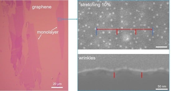
After the transfer, the graphene/PDMS was stretched as a whole at 10 percent, as shown in the top panel of Figure 2a. Compared to the image of graphene on the Si wafer (lower panel of Figure 2a), the graphene on the PDMS film is fractured in the transverse direction (top panel of Figure 2a), confirming the existence of tension in graphene in the vertical direction. The enlarged image of the graphene surface shows that buckling deformation did occur. For example, Figure 2b shows the buckling phenomena in three-layer graphene. To achieve better experimental characterization, we prepared cross-sections of the buckling patterns using FIB technology (see Materials and Methods). The wrinkle-like profile of the cross-section indicates that the wrinkles do appear in the three-layer graphene (Figure 2c), but these wrinkles lack uniformity. Figure 2d is an enlarged image of another localized region in Figure 1a, which provides the buckling pattern of monolayer graphene. Further enlarging the image (lower panel of Figure 2d), we can find three wrinkles of the monolayer graphene, marked by several line segments, although they are very slight. The FIB image (Figure 2e) provides further evidence for the existence of the three wrinkles. These results together suggest that the buckling behavior of few-layer graphene on soft substrates can be well stimulated and maintained through directly stretching or compressing the bilayers of graphene membranes and soft films, even though the mechanical operation has a high percentage of stretching or compression.
3.3. Calculation of Young’s Modulus for Graphene with Different Layers
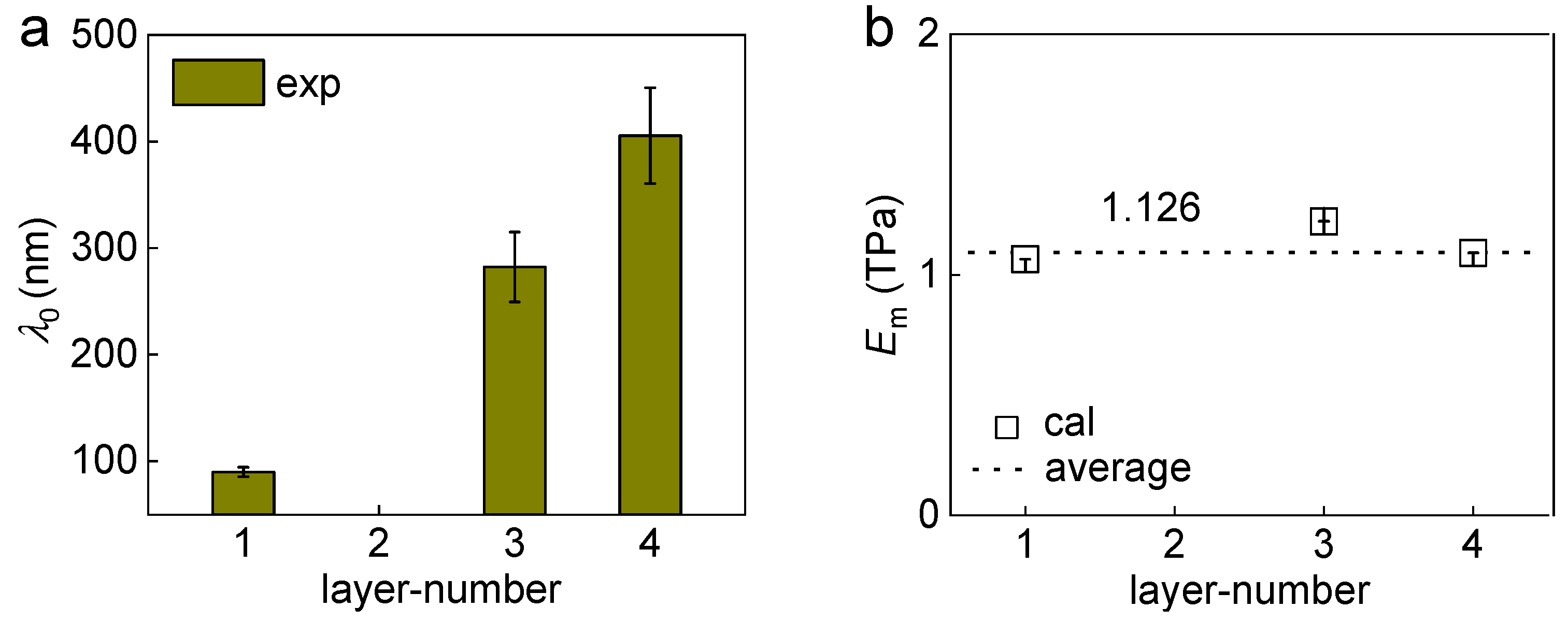
The surface perimeter of a wrinkle can be accurately captured based on its cross-section. Figure 3a shows the statistical results of the surface perimeter of wrinkles in few-layer graphene, which are 89.9 ± 4.38406 nm, 282.36 ± 32.88028 nm, and 405.5 ± 43 nm in monolayer, three-layer, and four-layer graphene, respectively. The very large standard deviations of the surface perimeter in two and four-layer graphene are attributed to the significant inhomogeneity of the wrinkling profile in these two graphene membranes, as shown in Figure S1. Even so, the surface perimeter of the wrinkles is shown to increase monotonically with the thickness of the graphene membrane, tm, corresponding to the number of graphene layers.
The surface perimeter of the wrinkle is equal to the intrinsic periodic length, λ0 (μm), of the wrinkling instability threshold in the stiff and soft bilayer system. If the thickness contrast of the soft film to the stiff membrane is sufficiently large, λ0 is proportional to the thickness of the stiff membrane, tm, and independent of the thickness of the soft film, ts, expressed as follows [22,23]
where A is a material constant of the stiff/soft bilayer films determined by Young’s modulus and Poisson ratios of the stiff membranes and soft films. Es (GPa), μs, ts (μm) and Em (GPa), μm, tm (nm) are Young’s modulus, Poisson’s ratio, and thickness of the soft film and stiff membrane, respectively. The detailed derivation of Equation (1) is given in Ref. [22].
For the simplicity of Equation (1) derivation, the thickness of the soft layer was approximated as infinite. In our graphene/PDMS bilayer systems, ts ranges from tens to hundreds of microns, while tm is below 1 nanometer. Thus, ts is larger than tm by four orders of magnitude. Therefore, the thickness approximation is reasonable within the scope of this paper. When the two thicknesses are close to each other, the critical wavelength (λ0) is determined by both the thicknesses of the stiff membrane and soft film [24,25,26,27].
According to Equation (1), Young’s modulus of the stiff membrane (Em) can be written as follows
Now, the modulus of graphene with different layers can be evaluated according to Equation (2) because the thickness of the monolayer graphene is known and the intrinsic periodic length, λ0, of few-layer graphene can be determined in the experiment. μm = 0.165, μs = 0.48, Es = 1.8 MPa, and the thickness of monolayer graphene is equal to 0.335 nm in the following calculation [11]. Figure 3b shows the calculated moduli of few-layer graphene, which are 1.06517 ± 0.00012 TPa, 1.22232 ± 0.00019 TPa, and 1.09115 ± 0.00017 TPa for the monolayer, three-layer, and four-layer graphene, respectively. These calculated results are close to each other, with an average value of 1.12621 ± 0.00016 TPa, which is close to the common modulus of monolayer graphene of 1 TPa. These results demonstrate that Young’s modulus of graphene is independent of the number of graphene layers if the number of layers is below four.
It should be pointed out that micromechanics models can also be used to estimate Young’s moduli of the stiff membrane, which are called “Tsai-Wu” and “Checkboard” [28,29]. Our work provides an alternative approach to estimating Young’s modulus of stiff membranes on soft substrates, which can be complementary to previous approaches.
4. Conclusions
The wrinkle pattern of few-layer graphene on a soft substrate can be well stimulated and maintained through directly stretching or compressing the bilayer of graphene membrane and soft film. Based on the buckling behavior, the moduli of the graphene with layers less than four are calculated, which are independent of the number of graphene layers and close to each other, with an average value of 1.12621 TPa. The buckling deformation of other 2D materials can be also well achieved based on a stiff/soft bilayer system and mechanical manipulation, which allows strain-dependent physical or chemical properties of the 2D materials to be well investigated.
Supplementary Materials
The following supporting information can be downloaded at https://www.mdpi.com/article/10.3390/coatings12121983/s1, Figure S1: Buckling behavior of four-layer graphene.
Author Contributions
Conceptualization, Y.M.; methodology, Y.M.; software, J.Z.; investigation, Y.M.; data curation, Y.M., B.L., and L.L.; writing original draft preparation, Y.M. All authors have read and agreed to the published version of the manuscript.
Funding
This work was supported by the Fellowship of China national postdoctoral program for innovative talents (BX20200166), the Natural Science Foundation of Jiangsu Province (BK20210271), the Postdoctoral Science Foundation of Jiangsu Province (2020Z355), National Natural Science Foundation of China (12202189), China Postdoctoral Science Foundation (2021M701703), and Jiangsu Funding Program for Excellent postdoctoral talent (2022ZB211).
Institutional Review Board Statement
Not applicable.
Informed Consent Statement
Not applicable.
Data Availability Statement
Not applicable.
Conflicts of Interest
The authors declare no conflict of interest.
References
- Novoselov, K.S.; Geim, A.K.; Morozov, S.V.; Jiang, D.; Zhang, Y.; Dubonos, S.V.; Grigorieva, I.V.; Firsov, A.A. Electric field effect in atomically thin carbon films. Science 2004, 306, 666–669. [Google Scholar] [CrossRef] [PubMed] [Green Version]
- Georgakilas, V.; Otyepka, M.; Bourlinos, A.B.; Chandra, V.; Kim, N.; Kemp, K.C.; Hobza, P.; Zboril, R.; Kim, K.S. Functionalization of graphene: Covalent and non-covalent approaches, derivatives and applications. Chem. Rev. 2012, 112, 6156–6214. [Google Scholar] [CrossRef] [PubMed]
- Tang, X.; Yang, W.; Yin, S.; Tai, G.; Su, M.; Yang, J.; Shi, H.; Wei, D.; Yang, J. Controllable Graphene Wrinkle for a High-Performance Flexible Pressure Sensor. ACS Appl. Mater. Interfaces 2021, 13, 20448–20458. [Google Scholar] [CrossRef] [PubMed]
- Chung, J.W.; Ko, Y.H.; Hong, Y.K.; Song, W.; Jung, C.; Tang, H.; Lee, J.; Lee, M.h.; Lee, B.-l.; Park, J.-i.; et al. Flexible nano-hybrid inverter based on inkjet-printed organic and 2D multilayer MoS2 thin film transistor. Org. Electron. 2014, 15, 3038–3042. [Google Scholar] [CrossRef]
- Ma, Y.; Zhang, Y.; Cai, S.; Han, Z.; Liu, X.; Wang, F.; Cao, Y.; Wang, Z.; Li, H.; Chen, Y.; et al. Flexible Hybrid Electronics for Digital Healthcare. Adv. Mater. 2020, 32, e1902062. [Google Scholar] [CrossRef]
- Khang, D.Y.; Jiang, H.Q.; Huang, Y.; Rogers, J.A. A stretchable form of single-crystal silicon for high-performance electronics on rubber substrates. Science 2006, 311, 208–212. [Google Scholar] [CrossRef] [Green Version]
- Liu, Z.; Gong, Y.; Zhou, W.; Ma, L.; Yu, J.; Idrobo, J.C.; Jung, J.; MacDonald, A.H.; Vajtai, R.; Lou, J.; et al. Ultrathin high-temperature oxidation-resistant coatings of hexagonal boron nitride. Nat. Commun. 2013, 4, 2541. [Google Scholar] [CrossRef] [Green Version]
- Wang, C.; Liu, Y.; Lan, L.; Tan, H. Graphene wrinkling: Formation, evolution and collapse. Nanoscale 2013, 5, 4454–4461. [Google Scholar] [CrossRef]
- Alden, J.S.; Tsen, A.W.; Huang, P.Y.; Hovden, R.; Brown, L.; Park, J.; Muller, D.A.; McEuen, P.L. Strain solitons and topological defects in bilayer graphene. Proc. Natl. Acad. Sci. USA 2013, 110, 11256–11260. [Google Scholar] [CrossRef] [Green Version]
- Wang, L.; Liu, X.; Zang, J. Mechanically tunable terahertz graphene plasmonics using soft metasurface. 2D Mater. 2016, 3, 041007. [Google Scholar] [CrossRef]
- Meng, L.; Su, Y.; Geng, D.; Yu, G.; Liu, Y.; Dou, R.-F.; Nie, J.-C.; He, L. Hierarchy of graphene wrinkles induced by thermal strain engineering. Appl. Phys. Lett. 2013, 103, 251610. [Google Scholar] [CrossRef] [Green Version]
- Sampathkumar, K.; Androulidakis, C.; Koukaras, E.N.; Rahova, J.; Drogowska, K.; Kalbac, M.; Vetushka, A.; Fejfar, A.; Galiotis, C.; Frank, O. Sculpturing graphene wrinkle patterns into compliant substrates. Carbon 2019, 146, 772–778. [Google Scholar] [CrossRef]
- Androulidakis, C.; Koukaras, E.N.; Sampathkumar, K.; Rahova, J.; Galiotis, C.; Frank, O. Hierarchy of nanoscale graphene wrinkles on compliant substrate: Theory and experiment. Extreme Mech. Lett. 2020, 40, 100948. [Google Scholar] [CrossRef]
- Lee, W.K.; Kang, J.; Chen, K.S.; Engel, C.J.; Jung, W.B.; Rhee, D.; Hersam, M.C.; Odom, T.W. Multiscale, Hierarchical Patterning of Graphene by Conformal Wrinkling. Nano Lett. 2016, 16, 7121–7127. [Google Scholar] [CrossRef] [PubMed]
- Wang, W.; Yang, S.; Wang, A. Strain induced highly oriented graphene wrinkles. Mater. Res. Express 2017, 4, 075601. [Google Scholar] [CrossRef]
- Wang, C.; Lan, L.; Tan, H. The physics of wrinkling in graphene membranes under local tension. Phys. Chem. Chem. Phys. 2013, 15, 2764–2773. [Google Scholar] [CrossRef] [PubMed]
- Huang, M.Y.; Yan, H.G.; Chen, C.Y.; Song, D.H.; Heinz, T.F.; Hone, J. Phonon softening and crystallographic orientation of strained graphene studied by Raman spectroscopy. Proc. Natl. Acad. Sci. USA 2009, 106, 7304–7308. [Google Scholar] [CrossRef] [Green Version]
- Meng, Y.; Zhang, S.; Wu, K.; Li, J.; Li, L. Mechanically Tunable Bilayer Composite Grating for Unique Light Manipulation and Information Storage. Adv. Opt. Mater. 2019, 7, 1801017. [Google Scholar] [CrossRef]
- Meng, Y.; Gong, X.; Huang, Y.; Li, L. Mechanically tunable opacity effect in transparent bilayer film: Accurate interpretation and rational applications. Appl. Mater. Today 2019, 16, 474–481. [Google Scholar] [CrossRef]
- Cairney, J.M.; Munroe, P.R.; Hoffman, M. The application of focused ion beam technology to the characterization of coatings. Surf. Coat. Technol. 2005, 198, 165–168. [Google Scholar] [CrossRef]
- Lee, J.; Lee, H.; Jeong, N.; Park, D.; Choi, I.; Chung, H. High-speed residue-free transfer of two-dimensional materials using PDMS stamp and water infiltration. Curr. Appl. Phys. 2020, 20, 1190–1194. [Google Scholar] [CrossRef]
- Zhuo, L.; Zhang, Y. The mode-coupling of a stiff film/compliant substrate system in the post-buckling range. Int. J. Solids Struct. 2015, 53, 28–37. [Google Scholar] [CrossRef]
- Meng, Y.; Xiang, H.; Zhang, J.; Hu, Z.; Yin, J.; Li, L.; Zhang, Z.; Guo, W. Quantized buckling evolution routes and fracture in stiff/soft bilayer films. Res. Sq. 2021, 2. [Google Scholar] [CrossRef]
- Vandeparre, H.; Damman, P. Wrinkling of stimuloresponsive surfaces: Mechanical instability coupled to diffusion. Phys. Rev. Lett. 2008, 101, 124301. [Google Scholar] [CrossRef] [PubMed] [Green Version]
- Cerda, E.; Mahadevan, L. Geometry and physics of wrinkling. Phys. Rev. Lett. 2003, 90, 074302. [Google Scholar] [CrossRef] [Green Version]
- Vandeparre, H.; Leopoldes, J.; Poulard, C.; Desprez, S.; Derue, G.; Gay, C.; Damman, P. Slippery or sticky boundary conditions: Control of wrinkling in metal-capped thin polymer films by selective adhesion to substrates. Phys. Rev. Lett. 2007, 99, 188302. [Google Scholar] [CrossRef]
- Huang, Z.Y.; Hong, W.; Suo, Z. Nonlinear analyses of wrinkles in a film bonded to a compliant substrate. J. Mech. Phys. Solids 2005, 53, 2101–2118. [Google Scholar] [CrossRef]
- Kabir, H.; Aghdam, M.M. A robust Bézier based solution for nonlinear vibration and post-buckling of random checkerboard graphene nano-platelets reinforced composite beams. Compos. Struct. 2019, 212, 184–198. [Google Scholar] [CrossRef]
- Li, S.; Sitnikova, E.; Liang, Y.; Kaddour, A.-S. The Tsai-Wu failure criterion rationalised in the context of UD composites. Compos. Part A Appl. Sci. Manuf. 2017, 102, 207–217. [Google Scholar] [CrossRef]
Figure 1.
Schematical illustration of the process of transferring graphene to PDMS film. (a) Top panel, mechanical exfoliation, fabrication of few-layer graphene on Si wafer. Lower panel, optical microscopy image showing the few-layer graphene on the Si wafer. (b) Spinning PMMA solution on the graphene/Si wafer. (c) Etching SiO2 from the Si wafer using a mixture of 5%–10% hydrofluoric acid and ethanol. (d) Graphene/PMMA bilayer. (e) Spinning PDMS solution on the graphene/PMMA bilayer. (f) Etching PMMA using acetone solution. (g) Graphene/PDMS bilayer.

Figure 2.
Experimental results on the buckling behavior of few-layer graphene. (a) Top panel, scanning electron microscopy (SEM) image showing a bilayer of graphene/PDMS with mechanical stretching of 10%. Lower panel, the graphene on the Si wafer, the same as the lower panel of Figure 1a. (b) Enlarged image of the light blue dotted frame region in (a), showing the buckling behavior of the three-layer graphene. (c) Top panel, focused ion beam (FIB) image showing the cross-section of wrinkles of three-layer graphene, with the milled location marked by a red line in (b). Lower panel, enlarged image of the red dotted frame region in the top panel. “Pt” indicates platinum film, which is needed to mill the cross-section by FIB. The cross-section of the few-layer graphene is marked by a white dotted line. (d) SEM images, top panel, enlarged image of the black dotted frame region in (a) showing the wrinkle pattern in monolayer graphene. Lower panel, enlarged image of the three wrinkles marked with red dotted frame on the top panel. (e) FIB image showing the cross-section of three wrinkles in monolayer graphene.
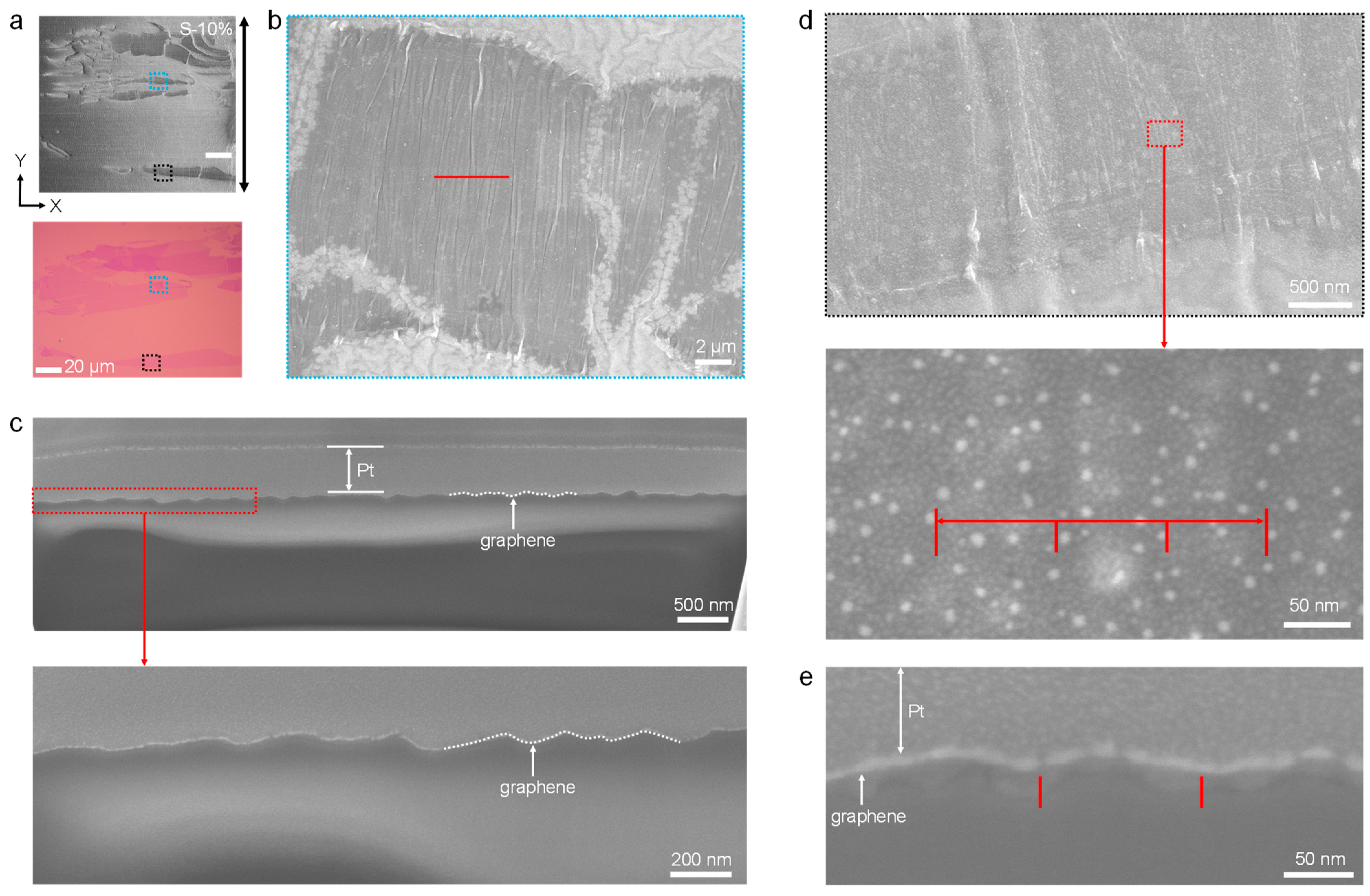
Figure 3.
Statistical results for the surface perimeter and modulus of few-layer graphene. (a) The surface perimeter of wrinkles in few-layer graphene. (b) Calculated Young’s modulus, Em, of few-layer graphene.
Figure 3.
Statistical results for the surface perimeter and modulus of few-layer graphene. (a) The surface perimeter of wrinkles in few-layer graphene. (b) Calculated Young’s modulus, Em, of few-layer graphene.

Table 1.
Elastic properties of the three films.
| Film | Young’s Modulus (GPa) | Poisson’s Ratio |
|---|---|---|
| PDMS | 0.0018 | 0.48 |
| PMMA | 2 | 0.3 |
| Graphene [11] | 1000 | 0.165 |
Publisher’s Note: MDPI stays neutral with regard to jurisdictional claims in published maps and institutional affiliations. |
© 2022 by the authors. Licensee MDPI, Basel, Switzerland. This article is an open access article distributed under the terms and conditions of the Creative Commons Attribution (CC BY) license (https://creativecommons.org/licenses/by/4.0/).
Share and Cite
MDPI and ACS Style
Meng, Y.; Li, B.; Li, L.; Zhang, J. Buckling Behavior of Few-Layer Graphene on Soft Substrate. Coatings 2022, 12, 1983. https://doi.org/10.3390/coatings12121983
AMA Style
Meng Y, Li B, Li L, Zhang J. Buckling Behavior of Few-Layer Graphene on Soft Substrate. Coatings. 2022; 12(12):1983. https://doi.org/10.3390/coatings12121983
Chicago/Turabian StyleMeng, Yancheng, Baowen Li, Luxian Li, and Jianqiang Zhang. 2022. "Buckling Behavior of Few-Layer Graphene on Soft Substrate" Coatings 12, no. 12: 1983. https://doi.org/10.3390/coatings12121983
Note that from the first issue of 2016, this journal uses article numbers instead of page numbers. See further details here.