
Comparison of Cobalt Integration with Various Dielectric Materials under Thermal and Electrical Stress


1
Department of Electrical Engineering, National Chi-Nan University, Nan-Tou 54561, Taiwan, R.O.C.
2
Department of Materials Science and Engineering, Feng Chia University, Taichung 40724, Taiwan, R.O.C.
3
Department of Materials Science and Engineering, National Formosa University, Huwei 63201, Taiwan, R.O.C.
*
Author to whom correspondence should be addressed.
Coatings 2023, 13(10), 1818; https://doi.org/10.3390/coatings13101818
Submission received: 14 June 2023
/
Revised: 3 October 2023
/
Accepted: 17 October 2023
/
Published: 23 October 2023
Abstract
:Cobalt (Co) is proposed to replace copper (Cu) as a conductor in the back-end-of-line (BEOL) interconnects of integrated circuits. In this study, the electric characteristics and reliability of the integration of Co with various dielectric films (SiO2, dense, and porous low-k SiOCH films) under thermal and electrical stress were compared. Thermal annealing repaired sputtering-Co-deposition-induced damage to the dielectric film but reduced the breakdown field and time-dependence-dielectric-breakdown (TDDB) times due to the diffusion of Co atoms. After annealing, the SiO2 film had the largest reductions in the breakdown field, TDDB failure time, and electric field acceleration factor, indicating that the diffusion of Co atoms dominates in the oxygen-rich surface. Under electrical stress, the drift of Co atoms favors the porous low-k film with the assistance of porosity. As a result, a barrier is required for Co metallization. To achieve barrier-free or barrier-less processing in Co metallization, the dense low-k film is the best option to integrate with Co.
Keywords:
cobalt; SiO2; low dielectric constant; porous low-k; thermal stress; electrical stress; metal drift1. Introduction
As the feature size of integrated circuits (ICs) is continuously scaling down, the resistance–capacitance (RC) delay of the back-end-of-line (BEOL) interconnects has become a limiting factor in the performance of ICs [1,2]. As a result, copper (Cu) and low dielectric constant (low-k) materials have replaced the traditional use of Al and SiO2 as conductor and insulator materials in the BEOL interconnects, since the development of the 0.18 μm technology node, in order to reduce the RC delay [3,4,5].
The continuous scaling of the dimensions of BEOL interconnects with the technology node resulted in an increase in the capacitance, thus requiring further reduction to the dielectric constant (k) of low-k films. The reduction of the k of low-k film could be achieved by introducing porosity into the film; the result of this is called the porous low-k film. On the other hand, the porous low-k films have weak mechanical, thermal, and electrical characteristics, thereby leading to more processing challenges and the degradation of electric performance and reliability as they are integrated into BEOL interconnects [4,5,6,7].
As the technology node advances to 10 nm and below, a dramatic increase in the resistivity of Cu conductors in the scaling interconnects has become a critical issue [8,9,10]. Additionally, a barrier against Cu migration would occupy a larger cross-sectional area of the metal line as the dimension of the BEOL interconnects is continuously scaling down [11,12]. Such barriers have a high resistivity, further increasing the line resistance and RC delay.
To mitigate the increase in line resistance due to the scaling effect, an alternative conductor in the BEOL interconnects to substitute Cu has been proposed. The candidates to replace Cu must have lower product values of bulk resistivity (ρ0) and electron mean free path (λ) than Cu in order to exhibit higher conductivity in the limit of a small line width [13,14,15,16]. Based on this rule, the potential candidates are Mo, Co, Ni, and Ru [15,16,17,18]. Among these potential candidates, Co has gained more attention because its resistivity is less sensitive to scaling [19]. Additionally, Co is expected to have better resistance against electromigration than Cu because it has a higher melting temperature (1495 °C) than Cu (1085 °C) [17,18]. Moreover, Co does not require high-resistivity nucleation layers and its grain growth can be achieved by annealing at a low temperature [16]. Last and most importantly, the migration of Co is weaker than that of Cu, thereby achieving barrier-less or barrier-free processing for Co metallization. This provides an acceptable line- or via-resistance [19,20]. Most studies indicated that Co would drift under electrical stress, with the magnitude being less than Cu; however, the integration dielectric film used was SiO2 film [21,22]. On the other hand, studies related to Co/low-k integration are limited.
Here, various dielectric films, including SiO2, dense, and porous low-k dielectric films, were integrated with Co in this study. After being subjected to thermal and electrical stress, the electrical characteristics and reliability of the integration schemes were characterized and compared.
2. Experimental Details
2.1. Sample Preparation
In this study, SiO2, dense, and porous low-k dielectric films were deposited on p-type (100) silicon substrates as the starting materials. SiO2 films were grown by using a dry oxidation method in a furnace at 1100 °C. Both the dense and porous low-k dielectric films were SiOCH materials, which were deposited in a plasma-enhanced chemical vapor deposition (PECVD) reactor (Applied Material Corp. producer system, Santa Clara, CA, USA). Diethoxymethylsilane (DEMS) and oxygen (O2) were used as the matrix precursors during the deposition. For the production of porous low-k films, alpha-terpinene (ATRP), as a porogen precursor, was also introduced into the reactor. The organic porogen in the low-k film was then removed by performing UV thermal-assisted curing after deposition. This led to the formation of pores in the film. Details about the deposition conditions for the production of dense and porous low-k films can be found elsewhere [23,24]. The properties of SiO2, dense, and porous low-k dielectric films are listed in Table 1. The thickness of all studied films was controlled at 130 ± 10 nm. The dielectric constant (k) values were 4.02 ± 0.03, 3.02 ± 0.05, and 2.56 ± 0.08 for the pristine SiO2, dense, and porous low-k dielectric films, as determined by the Hg probe C–V measurement (5100 CV system).
Following this, metal-insulator-silicon (MIS; Co/dielectric/Si) capacitors for electrical and reliability measurements were fabricated. Co was sputtering deposited onto a dielectric film through a showdown mask in the direct current (DC) magnetron sputtering system at room temperature. The base pressure in the sputtering chamber was 4.0 × 10⁻⁴ Pa. During the deposition, the working pressure was 0.53 Pa, with the introduction of Ar at a gas flow rate of 20 sccm. The DC power was kept at 50 W. The deposition thickness of Co was approximately 100 nm. The formation Co dot was square, with an area of 9.0 × 10⁻⁴ cm2. To evaluate electrical and reliability characteristics under thermal stress, parts of the fabricated MIS capacitors were annealed in N2 environments at 425 °C for 2 h.
2.2. Sample Characterization
The thickness of the studied films was determined by using an optical-probe system with an ellipsometer (Film TekTM 3000SE, Keithley, 6517A, Austin, TX, USA). Electrical and reliability characteristics, including capacitance–voltage (C–V), current–voltage (I–V), and time-dependence-dielectric-breakdown (TDDB) were conducted on the fabricated MIS capacitors. The C–V measurement was operated at a frequency of 1 MHz by using a semiconductor parameter analyzer (HP4280A). The k value of a dielectric film and the flat-band voltages (Vfb) in the Co-gate MIS capacitor can be determined from the measured C-V curves. The I–V and TDDB characteristics were measured by using an electrometer (Keithley 6517A). The I–V measurements were performed using a ramp-voltage-sweep (RVS) method to measure the leakage current and breakdown voltage (field). The TDDB test was used to evaluate the long-term reliability of a dielectric film. During the TDDB test, a constant electric field was continuously applied and the leakage current was monitored with stressing time. As the leakage current suddenly increased by at least three orders of magnitude, a dielectric breakdown occurred; the stressing time was defined as the TDDC failure time. To evaluate the drift of Co into the dielectric film under electrical stress, an electric field at positive polarity was applied to the Co-gate of the MIS capacitors for 100 s. After being subjected to electrical stress, the samples were measured for I–V characteristics. The measurements were conducted at room temperature (25 °C). To prevent moisture absorption and metal gate oxidation, a nitrogen gas purge was performed during the measurements.
3. Results and Discussion
Figure 1a–c plot the double direction C–V curves of the Co-gate MIS capacitors with SiO2, dense, and porous low-k dielectric films, respectively, before and after annealing at 425 °C for 2 h. For all samples, the measured capacitances were accumulation, transition, and depletion capacitances in order when voltage swept from negative to positive, which are typical p-type MIS C–V characteristics. Double-direction C–V curves were measured by sweeping voltage either from accumulation mode to inversion mode (forward voltage sweep; FVS) or from inversion mode to accumulation mode (reverse voltage sweep; RVS). Under either a FVS or RVS measurement, the measured accumulation capacitances were identical for all MIS capacitors with various dielectric films. After annealing, the accumulation capacitances decreased for all samples. In the as-fabricated and annealed stages, the accumulation capacitance followed the order: SiO2 > dense > porous low-k.
The dielectric constant (k) of a dielectric film in the MIS capacitor can be determined through the measured accumulation capacitance (C) by using the expression of k = Cd/ε0A. Here, εo is absolute capacitive in a vacuum (8.85 × 10⁻¹² F/m), d is film thickness, and A is the area of the MIS capacitor. The pristine k values were 4.02 ± 0.03, 3.02 ± 0.05, and 2.56 ± 0.08 for the pristine SiO2, dense, and porous low-k dielectric films. As Co was integrated with these dielectric films, the k values increased to 4.51 ± 0.03, 4.34 ± 0.08, and 3.70 ± 0.08 for the SiO2, dense, and porous low-k films, respectively. An increased k value is believed to be caused by the sputtering deposition of Co metal. During the sputtering deposition of Co, plasma-generated active species damage the dielectric film, thereby increasing the capacitance and k value. [25,26]. After annealing, all accumulation capacitances decreased, thus reducing the k values to 4.10 ± 0.02, 3.24 ± 0.06, and 2.97 ± 0.05 for SiO2, dense, and porous low-k dielectric films, respectively. This result suggests that sputtering-deposition-induced damage on a dielectric film can be repaired by annealing. To evaluate the damage effect induced by sputtering deposition and the repair efficiency caused by annealing, the relative k values (relative to the k value of the pristine film) for SiO2, dense, and porous low-k films before and after annealing were plotted in Figure 2. As shown, the relative k values were higher than 1.0 for all as-fabricated and annealed films, revealing that the capacitance would inevitably increase as Co is integrated with a dielectric film. After Co deposition by sputtering deposition, porous low-k films had the largest relative k values and SiO2 films had the smallest relative k values, representing more plasma-induced damage on the porous low-k films and less plasma-induced damage on the SiO2 films. The degree of plasma-induced damage is strongly dependent on the structure of a dielectric film [27]. After annealing, the relative k values reduced, demonstrating that the Co-sputtering-deposition-induced damage can be repaired by annealing. However, the k values were still higher than the pristine values, implying that such damage cannot be repaired completely. Similarly, the porous low-k film had the largest value (1.16), suggesting that the recovery of plasma-induced damage by annealing is not effective for the porous low-k film compared to the SiO2 and dense low-k films.
Turning attention to the C−V curves shown in Figure 1, the flat-band voltages (Vfb) and the hysteresis (e.g., the difference in Vfb between FVS and RVS C−V curves) can be determined. In the ideal MIS capacitor, the Vfb value is the difference in work function between the metals and the Si if the dielectric insulator has no charges. Theoretically, the work functions of p-type Si and Co are 5.25 eV and 5.00 eV, respectively [28]. As a result, the Vfb value of the Co-gate MIS capacitor is estimated to be −0.25 eV. In a real case, the thermally grown SiO2 film reportedly has positive charges in the order of 1010–1011 cm−2, corresponding to the negative Vfb shift of approximately 0.01–0.1 V [29]. As a result, the Vfb value was −0.25 –−0.35 V. In this study, for as-deposited Co-gate MIS capacitors with SiO2 film, the Vfb value was determined to be −13.68 V and no hysteresis was observed, revealing that positive charges are introduced into the SiO2 film during the fabrication of the Co-gate MIS capacitor. After annealing, the Vfb value reduced to −1.0~−2.5 V but a hysteresis was detected. It is believed that sputtering-deposition-induced charges during Co deposition can be removed by annealing [30], making the Vfb value return back to approaching the ideal value. For the origin of the hysteresis, (a) electron (e−) trapping; (b) hole (h+) or positive charges trapping; (c) mobile charges; and (d) as-grown traps are the possible sources [31]. For Co-gate MIS capacitors with SiO2 film, the Vfb shifted toward a negative voltage direction after annealing. As a result, the hysteresis increased to 2.52 V after annealing, which is likely to be caused by positive charges trapping (e.g., Co ions).
For both dense and porous low-k films, donor-like traps were reportedly generated in the bulk film during the deposition [31]. Additionally, charges were introduced into the dielectric film during the fabrication of the Co-gate MIS capacitor. Hence, a larger Vfb hysteresis was expected. After annealing, Co-sputtering-deposition-induced charges can be partially removed and Co ions may diffuse into the films. Hence, the Vfb hysteresis becomes more complex. Therefore, detailed research to verify the mechanism is required. Figure 3 compares the hysteresis of Co-gate MIS capacitors with SiO2, dense, and porous low-k dielectric films before and after annealing. For dense and porous low-k films, the hysteresis reduced while the hysteresis increased for SiO2 films. This suggests that the diffusion of Co ions was in progress within the SiO2 film during annealing.
Figure 4 plots the leakage current versus the electric-field (I–E) curves of MIS capacitors with various dielectric films before and after annealing. For the SiO2 film, the leakage current remained constant at 10−11 A with the electric field being increased. For both dense and porous low-k films, an obvious increase in the leakage current with the applied field was observed. The dense low-k film had a higher leakage current than the porous film due to the bonding structure [23], suggesting that the leakage current is less sensitive to porosity. The applied field, at which the leakage current suddenly increases by at least three orders of magnitude to more than 10−2 A, is defined as the breakdown field of a dielectric film. As shown in Figure 4, the breakdown field followed the order of SiO2 > dense low-k > porous low-k, which is associated with porosity. After annealing, the leakage current decreased for both low-k films while it slightly increased for the SiO2 film. The repair of the sputtering-deposition-induced damage during Co deposition by annealing is likely to be responsible for the reduced leakage current. The increased leakage current in the annealed Co-gate MIS capacitor with SiO2 film suggests that another mechanism dominates. Moreover, the breakdown field of all dielectric films reduced after annealing.
Figure 5 compares the breakdown fields of SiO2, dense, and porous low-k dielectric films in the Co-gate MIS capacitors before and after annealing. Here, the presented data were collected from ten samples. The calculated reduction magnitudes of the breakdown field after annealing are also listed in Figure 5. Before and after annealing, the breakdown field followed the same order: SiO2 > dense low-k > porous low-k. The breakdown field reduced after annealing for all dielectric films. Notably, the SiO2 film had the largest reduction magnitude. Based on the studies [32], the breakdown field would not be degraded by annealing until 450 °C for SiO2, dense, and porous low-k dielectric films, provided no extrinsic factor (i.e., metal diffusion) occurs. Here, the reduction in the breakdown field after annealing at 425 °C indicates that the diffusion of Co occurs in all dielectric films in this study. The largest reduction being for the SiO2 films suggests that more Co diffuses into the film upon annealing. This reflects that an oxygen-rich surface in the SiO2 film favors the occurrence of Co diffusion [33].
Compared to the SiO2 film, both the dense and porous low-k films, which are carbon-doped SiO2 films, had a lower reduction in the breakdown field after annealing. This suggests that the doped carbon would slow down the diffusion of Co [34]. Additionally, the porous low-k film had a larger reduction in the breakdown field than the dense low-k film due to the presence of porosity. The porosity provides a free surface, which is typically a faster diffusion path than the bulk of the film, accelerating the diffusion of Co.
TDDB tests were carried out on the as-deposited and annealed Co-gate MIS capacitors to determine the failure time (tfailure) as he breakdown of a dielectric film occurs. Three electric fields were applied and the E model (tfailure ~exp(−γE)) was used to describe the breakdown behavior of a dielectric film [35,36]. Here, γ is the electric-field acceleration factor. Figure 6 plots the TDDB failure times of the as-deposited and annealed Co-gate MIS capacitors with SiO2, dense, and porous low-k dielectric films as a function of the applied electric field. The changes in the extracted γ values before and after annealing are plotted in Figure 7. After annealing, all Co-gate MIS capacitors with SiO2, dense, and porous low-k dielectric films exhibited reduced TDDB failure times and γ values. A pronounced reduction was observed in the SiO2 film. The change in the γ value is a useful indicator to determine the breakdown mechanism [34,37]. An unchanged γ value represents the identical breakdown mechanism while a reduced γ value is associated with the introduction of an extrinsic breakdown mechanism. This extrinsic mechanism for the Co-gate MIS capacitor after being subjected to thermal stress is likely to be the diffusion of Co atoms or ions. As a result, the diffusion of Co into the SiO2 film upon annealing is more pronounced than with the low-k film. Comparing with the dense and porous low-k films reveals that the former had a smaller change in the γ value upon annealing. The doped carbon and the dense structure in the dense low-k film prevent the injection and diffusion of Co. As a result, barrier-less or barrier-free processing is possibly achieved as Co is integrated with the dense low-k films. For SiO2 and porous low-k films integrated with Co, a barrier is required to prevent Co from diffusing into the film.
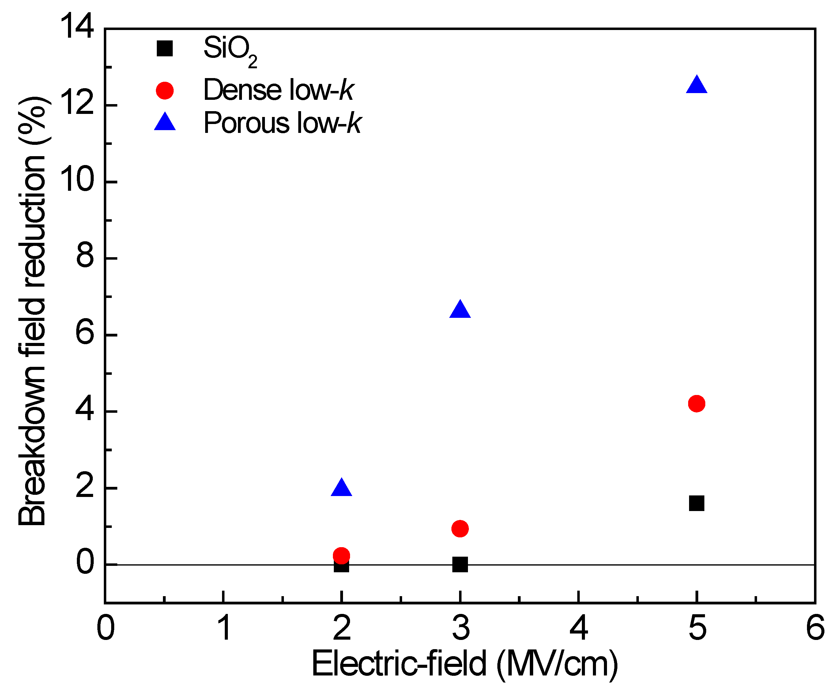
To evaluate the drift of Co into the film under electrical stress for SiO2, dense, and porous low-k dielectric films integrated with Co, positive-polarity fields were applied to the Co-gate MIS capacitors [38]. The stressing time was fixed at 102 s. After the application of the electrical stress, I–V measurements were conducted. Figure 8 plots the I–V curves of the Co-gate capacitor with the porous low-k film before and after electrical stress with electric fields of 2~5 MV/cm. After the application of positive-polarity electrical stress, a hump, in which the leakage sharply increased and then returned back, was formed. Moreover, this hump amplified with the applied electric field. This hump is believed to be the ionic current due to the migration of metal (Co) ions. First, positive-polarity electrical stress oxidizes Co to form ions; they then drift into the porous low-k film under the external electric field. Subsequently, a negative voltage sweep in the I–V measurement pushes the injected Co ions to drift back to the previous metal–dielectric interface. In addition to the presence of the hump, the breakdown field decreased and the reduction magnitude amplified with the increasing stressing field for the porous low-k film after electrical stress. These features reflect the drift of Co ions under electrical stress. For SiO2 and dense low-k films that underwent identical electrical stress, no hump was observed and a negligible reduction in the breakdown field was detected, indicating that the drift of Co ions was blocked. Figure 9 compares the reduction in the breakdown field for SiO2, dense, and porous low-k dielectric films in the Co-gate MIS capacitors after positive-polarity electrical stress as a function of the applied electric field. As shown, the porous low-k film had the largest reduction in the breakdown field and the SiO2 film had the lowest reduction, indicating that porosity and bonding in the film play a critical role in controlling Co ion migration under electrical stress. For the low-k films, the strength of Si–C bonding is relatively weak compared to that of Si–C bonding in the SiO2 film. As a result, electrical stress easily destroys Si–C bonding, leading to the drift of Co ions. Moreover, porosity in the low-k film further accelerates the drift of Co ions. As a result, the drift of Co ions into the porous low-k film under positive-polarity electrical stress is pronounced, thereby seriously degrading the electrical characteristics.
4. Conclusions
The electric characteristics and reliability of the integration of Co and various dielectric films under thermal and electrical stress have been investigated in this study. The sputtering deposition of Co induced damage on the dielectric film, thereby increasing the capacitance and k value. This increase was pronounced for the porous low-k film. Thermal annealing partially repaired the damage but reduced the breakdown field and TDDB characteristics due to the diffusion of Co. After annealing, the SiO2 film had the largest reduction due to the oxygen-rich surface, which favors the diffusion of Co. Under electrical stress, the drift of Co ions/atoms was serious in the porous low-k film due to the existence of porosity, thereby seriously degrading the electric characteristics. As a result, a barrier is required for SiO2 and porous low-k films when integrated with Co. To achieve barrier-free or barrier-less processing in Co metallization, the dense low-k film is the best option to integrate with Co.
Author Contributions
Conceptualization, Y.-L.C.; Methodology, H.-C.H.; Formal Analysis, W.-F.P., H.-C.H.; Investigation, W.-F.P., H.-C.H.; Validation, Y.-L.C., W.-F.P.; Writing—Original Draft Preparation, Y.-L.C.; Writing—Review & Editing, Y.-L.C.; G.-S.C., J.-S.F. All authors have read and agreed to the published version of the manuscript.
Funding
The authors would like to thank the Ministry of Science and Technology of the Republic of China, Taiwan, for financially supporting this research under contract MOST 111-2221-E-260-011-MY2.
Institutional Review Board Statement
Not applicable.
Informed Consent Statement
Not applicable.
Data Availability Statement
Not applicable.
Conflicts of Interest
The authors declare no conflict of interest.
References
- Kriz, J.; Angelkort, C.; Czekalla, M.; Huth, S.; Meinhold, D.; Pohl, A.; Schulte, S.; Thamm, A.; Wallace, S. Overview of dual damascene integration schemes in Cu BEOL integration. Microelectron. Eng. 2008, 85, 2128–2132. [Google Scholar] [CrossRef]
- Murarka, S.P. Low dielectric constant material for interlayer dielectric applications. Solid State Technol. 1996, 3, 83–88. [Google Scholar]
- Maex, K.; Baklanov, M.R.; Shamiryan, D.; Iacopi, F.; Brongersma, S.H.; Yanovitskaya, Z.S. Low dielectric constant materials for microelectronics. J. Appl. Phys. 2003, 93, 8793–8841. [Google Scholar] [CrossRef]
- Grill, A.; Gates, S.M.; Ryan, T.E.; Nguyen, S.V.; Priyadarshini, D. Progress in the development and understanding of advanced low k and ultralow k dielectrics for very large-scale integrated interconnects—State of the art. Appl. Phys. Rev. 2014, 1, 011306. [Google Scholar] [CrossRef]
- Croes, K.; Wilson, C.J.; Lofrano, M.; Beyer, G.P.; Tokei, Z. Interconnect reliability—A study of the effect of dimensional and porosity scaling. Microelectron. Eng. 2011, 88, 614–619. [Google Scholar] [CrossRef]
- Lionti, K.; Volksen, W.; Magbitang, T.; Darnon, M.; Dubois, G. Toward Successful Integration of Porous Low-k Materials: Strategies Addressing Plasma Damage. ECS J. Solid State Sci. Technol. 2015, 4, N3071. [Google Scholar] [CrossRef]
- Grill, A. Porous pSiCOH ultralow-k dielectrics for chip interconnects prepared by PECVD. Annu. Rev. Mater. Res. 2009, 39, 49–69. [Google Scholar] [CrossRef]
- Havemann, R.H.; Antonelli, G.A.; Arendt, G.K.; Danek, M.; McKerrow, A.J.; Weinberg, R.S. Copper BEOL solutions for advanced memory. Solid State Technol. 2009, 31, 10–15. [Google Scholar]
- Schuegraf, K.; Abraham, M.C.; Brand, A.; Naik, M.; Thakur, R. Semiconductor logic technology innovation to achieve sub-10 nm manufacturing. IEEE J. Electron Devices Soc. 2013, 1, 66–75. [Google Scholar] [CrossRef]
- Dutta, S.; Beyne, S.; Gupta, A.; Kundu, S.; Van Elshocht, S.; Bender, H.; Jamieson, G.; Vandervorst, W.; Bommels, J.; Wilson, C.J.; et al. Sub-100 nm2 Cobalt Interconnects. IEEE Electron Device Lett. 2018, 39, 731–734. [Google Scholar] [CrossRef]
- Wu, K.C.; Tseng, J.Y.; Chen, W.J. Electroplated Ru and RuCo films as a copper diffusion barrier. Appl. Surf. Sci. 2020, 516, 146139. [Google Scholar] [CrossRef]
- Steinhogl, W.; Schindler, G.; Steinlesberger, G.; Traving, M.; Engelhardt, M. Comprehensive study of the resistivity of copper wires with lateral dimensions of 100 nm and smaller. J. Appl. Phys. 2005, 97, 0237061. [Google Scholar] [CrossRef]
- Gall, D. Electron mean free path in elemental metals electron mean free path in elemental metals. J. Appl. Phys. 2016, 119, 085101. [Google Scholar] [CrossRef]
- Wislicenus, M.; Liske, R.; Gerlich, L.; Vasilev, B.; Preusse, A. Cobalt advanced barrier metallization: A resistivity composition analysis. Microelectron. Eng. 2015, 137, 11–15. [Google Scholar] [CrossRef]
- Zheng, J.-F.; Chen, P.; Baum, T.H.; Lieten, R.R.; Hunks, W.; Lippy, S.; Frye, A.; Li, W.; O’Neill, J.; Xu, J.; et al. Selective co growth on cu for void-free via fill. In Proceedings of the IEEE Interconnect Technology Conference/Materials for Advanced Metallization Conference (IITC/MAM), Grenoble, France, 18–21 May 2015; pp. 265–267. [Google Scholar]
- Hosseini, M.; Ando, D.; Sutou, Y.; Koike, J. Co and CoTix for contact plug and barrier layer in integrated circuits. Microelectron. Eng. 2018, 189, 78–84. [Google Scholar] [CrossRef]
- Chen, F.; Gardner, D. Influence of line dimensions on the resistance of Cu interconnections. IEEE Electron Device Lett. 1998, 19, 508–510. [Google Scholar] [CrossRef]
- He, M.; Zhang, X.; Nogami, T.; Lin, X.; Kelly, J.; Kim, H.; Spooner, T.; Edelstein, D.; Zhao, L. Mechanism of Co Liner as enhancement layer for Cu interconnect gap-fill. J. Electrochem. Soc. 2013, 160, D3040. [Google Scholar] [CrossRef]
- Yang, C.-C.; Spooner, T.; Ponoth, S.; Chanda, K.; Simon, A.; Lavoie, C.; Lane, M.; Hu, C.-K.; Liniger, E.; Gignac, L.; et al. Physical, Electrical, and Reliability Characterization of Ru for Cu Interconnects. In Proceedings of the 2006 IEEE International Interconnect Technology Conference, Burlingame, CA, USA, 5–7 June 2006; pp. 187–190. [Google Scholar]
- Dutta, S.; Kundu, S.; Gupta, A.; Jamieson, G.; Granados, J.F.; Bommels, J.; Wilson, C.J.; Tőkei, Z.; Adelmann, C. Highly scaled ruthenium interconnects. IEEE Electron Device Lett. 2017, 38, 949–951. [Google Scholar] [CrossRef]
- Pedreira, O.V.; Croes, K.; Leśniewska, A.; Wu, C.; Van Der Veen, M.H.; de Messemaeker, J.; Vandersmissen, K.; Jourdan, N.; Wen, L.G.; Adelmann, C.; et al. Reliability study on cobalt and ruthenium as alternative metals for advanced interconnects. In Proceedings of the IEEE International Interconnect Technology Conference, San Jose, CA, USA, 20–23 May 2014; pp. 173–176. [Google Scholar]
- Tierno, D.; Pedreira, O.V.; Wu, C.; Jourdan, N.; Kljucar, L.; Tőkei, Z.; Croes, K. Cobalt and Ruthenium drift in ultra-thin oxides. Microelectron. Reliab. 2019, 100–101, 113407. [Google Scholar] [CrossRef]
- Cheng, Y.L.; Lee, C.Y.; Huang, J.W.; Chen, G.S.; Fang, J.S. Comparison of various low dielectric constant materials. Thin Solid Films 2018, 660, 871–878. [Google Scholar] [CrossRef]
- Cheng, Y.L.; Lee, C.Y.; Hung, W.J.; Chen, G.S.; Fang, J.S. Electrical and reliability characteristics of dielectric stack with low dielectric constant SiCOH and capping SiCNH films. Surf. Coat. Technol. 2018, 350, 57–63. [Google Scholar] [CrossRef]
- Zhao, L.; Volders, H.; Baklanov, M.; Tokei, Z.; Pantouvaki, M.; Wilson, C.J.; Besien, E.V.; Beyer, G.P.; Claeys, C. Study of metal barrier deposition-induced damage to porous low-k materials. Microelectron. Eng. 2011, 88, 3030–3034. [Google Scholar] [CrossRef]
- Kaloyeros, A.E.; Eisenbraun, E. Ultrathin diffusion barriers/liners for gigascale copper metallization. Annu. Rev. Mater. Sci. 2000, 30, 363–385. [Google Scholar] [CrossRef]
- Baklanov, M.R.; de Marneffe, J.-F.; Shamiryan, D.; Urbanowicz, A.M.; Shi, H.; Rakhimova, T.V.; Huang, H.; Ho, P.S. Plasma processing of low-k dielectrics. J. Appl. Phys. 2013, 113, 041101. [Google Scholar] [CrossRef]
- He, M.; Lu, T.-M. Metal-Dielectric Interfaces in Gigascale Electronics: Thermal and Electrical Stability; Springer Series in Materials Science; Springer: New York, NY, USA, 2012; Volume 157. [Google Scholar]
- Hosseini, M.; Koike, J. Amorphous CoTix as a liner/diffusion barrier material for advanced copper metallization. J. Alloys Compd. 2017, 721, 134–142. [Google Scholar] [CrossRef]
- Cheng, Y.L.; Huang, H.C.; Lee, C.Y.; Chen, G.S.; Fang, J.S. Comparison of Cu and Co Integration with Porous Low-k SiOCH Dielectrics. Thin Solid Films 2020, 704, 138010. [Google Scholar] [CrossRef]
- Tang, B.J.; Croes, K.; Barbarin, Y.; Wang, Y.Q.; Degraeve, R.; Li, Y.; Toledano-Luque, M.; Kauerauf, T.; Bommels, J.; Tokei, Z.; et al. As-grown donor-like traps in low-k dielectrics and their impact on intrinsic TDDB reliability. Microelectron. Reliab. 2014, 54, 1675–1679. [Google Scholar] [CrossRef]
- Chang, Y.M.; Chang, W.Y.; Leu, J.; Cheng, Y.L. Effect of thermal treatment on physical, electrical properties and reliability of porogen-containing and porogen-free ultralow-k dielectric. Thin Solid Films 2013, 528, 67–71. [Google Scholar] [CrossRef]
- Huang, H.; McLaughin, P.S.; Kelly, J.J.; Yang, C.-C.; Southwick, R.G.; Wang, M.; Bonilla, G.; Karve, G. Time dependent dielectric breakdown of cobalt and ruthenium interconnects at 36nm pitch. In Proceedings of the IEEE International Reliability Physics Symposium (IRPS), Monterey, CA, USA, 31 March–4 April 2019; pp. 1–5. [Google Scholar]
- Zhao, L.; Volders, H.; Baklanov, M.; Tokei, Z.; Pantouvaki, M.; Wilson, C.J.; Besien, E.V.; Beyer, G.P.; Claeys, C. Impact of carbon-doping on time dependent dielectric breakdown of SiO2-based films. Appl. Phys. Lett. 2015, 106, 072902. [Google Scholar] [CrossRef]
- Mcpherson, J.W. Time dependent dielectric breakdown physics-Models revisited. Microelectron. Reliab. 2012, 52, 1753–1760. [Google Scholar] [CrossRef]
- Wu, E.Y.; Sune, J.; Vollertsen, R.P. Comprehensive physics-based breakdown model for reliability assessment of oxides with thickness ranging from 1 nm up to 12 nm. In Proceedings of the 2009 IEEE International Reliability Physics Symposium, Montreal, QC, Canada, 26-30 April 2009; pp. 708–717. [Google Scholar]
- Zhao, L.; Pantouvaki, M.; Croes, K.; Tőkei, Z.; Barbarin, Y.; Wilson, C.J.; Baklanov, M.R.; Beyer, G.P.; Claeys, C. Role of copper in time dependent dielectric breakdown of porous organo-silicate glass low-k materials. Appl. Phys. Lett. 2011, 99, 222110. [Google Scholar] [CrossRef]
- Fisher, I.; Eizenberg, M. Copper ion diffusion in porous and nonporous SiO2-based dielectrics using bias thermal stress and thermal stress tests. Thin Solid Films 2008, 516, 4111–4121. [Google Scholar] [CrossRef]
Figure 1.
C−V curves of Co-gate MIS capacitors before and after annealing: (a) SiO2; (b) dense low-k; (c) porous low-k films. (①: FVS; ②: RVS).
Figure 1.
C−V curves of Co-gate MIS capacitors before and after annealing: (a) SiO2; (b) dense low-k; (c) porous low-k films. (①: FVS; ②: RVS).

Figure 2.
Relative dielectric constant of SiO2, dense, and porous low-k dielectric films in Co-gate MIS capacitors before and after annealing.
Figure 2.
Relative dielectric constant of SiO2, dense, and porous low-k dielectric films in Co-gate MIS capacitors before and after annealing.

Figure 3.
Vfb hysteresis of SiO2, dense, and porous low-k dielectric films in Co-gate MIS capacitors before and after annealing.
Figure 3.
Vfb hysteresis of SiO2, dense, and porous low-k dielectric films in Co-gate MIS capacitors before and after annealing.
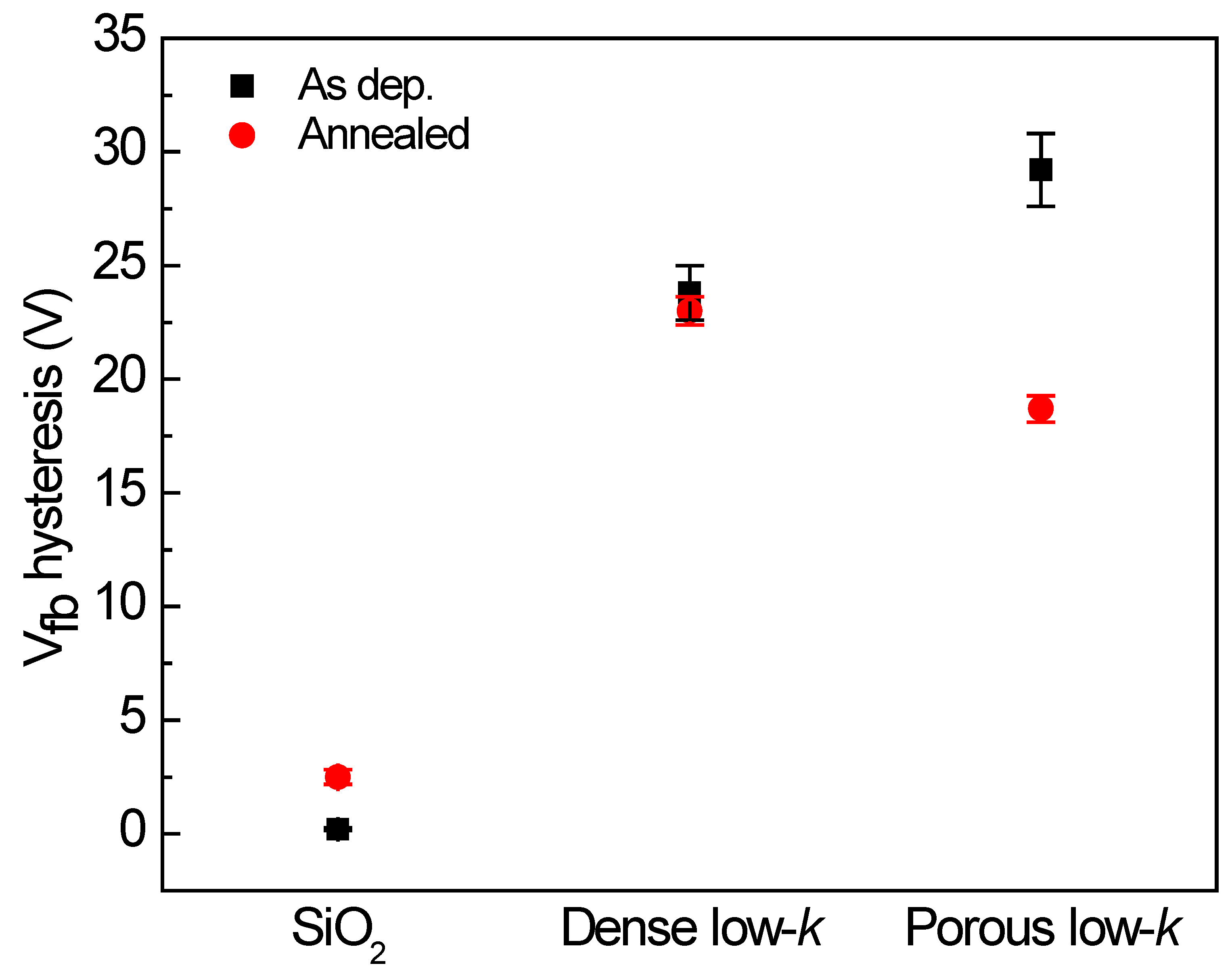
Figure 4.
I–E plots of SiO2, dense, and porous low-k dielectric films in Co-gate MIS capacitors before and after annealing.
Figure 4.
I–E plots of SiO2, dense, and porous low-k dielectric films in Co-gate MIS capacitors before and after annealing.
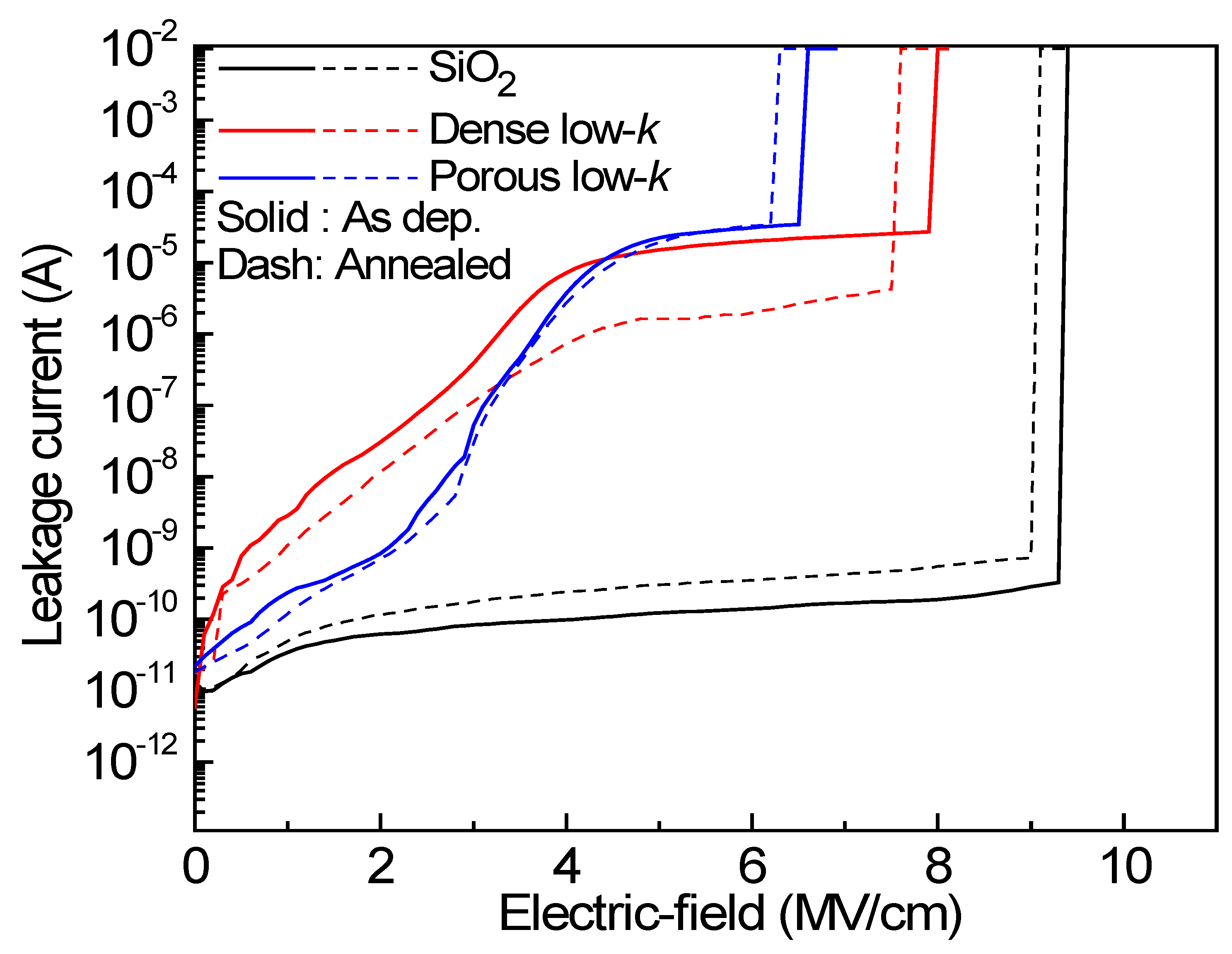
Figure 5.
Breakdown fields of SiO2, dense, and porous low-k dielectric films in Co-gate MIS capacitors before and after annealing.
Figure 5.
Breakdown fields of SiO2, dense, and porous low-k dielectric films in Co-gate MIS capacitors before and after annealing.
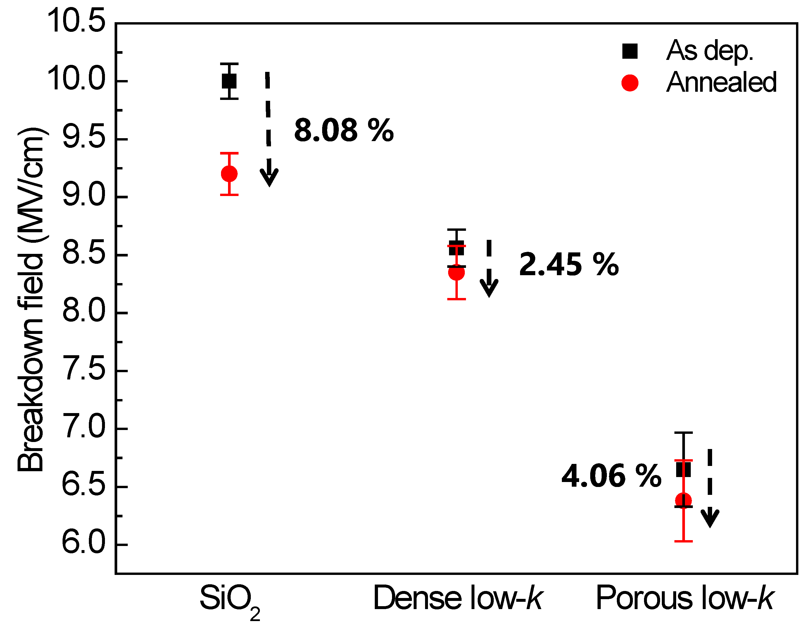
Figure 6.
TDDB failure times of SiO2, dense, and porous low-k dielectric films in Co-gate MIS capacitors before and after annealing as a function of stressing electric-field.
Figure 6.
TDDB failure times of SiO2, dense, and porous low-k dielectric films in Co-gate MIS capacitors before and after annealing as a function of stressing electric-field.
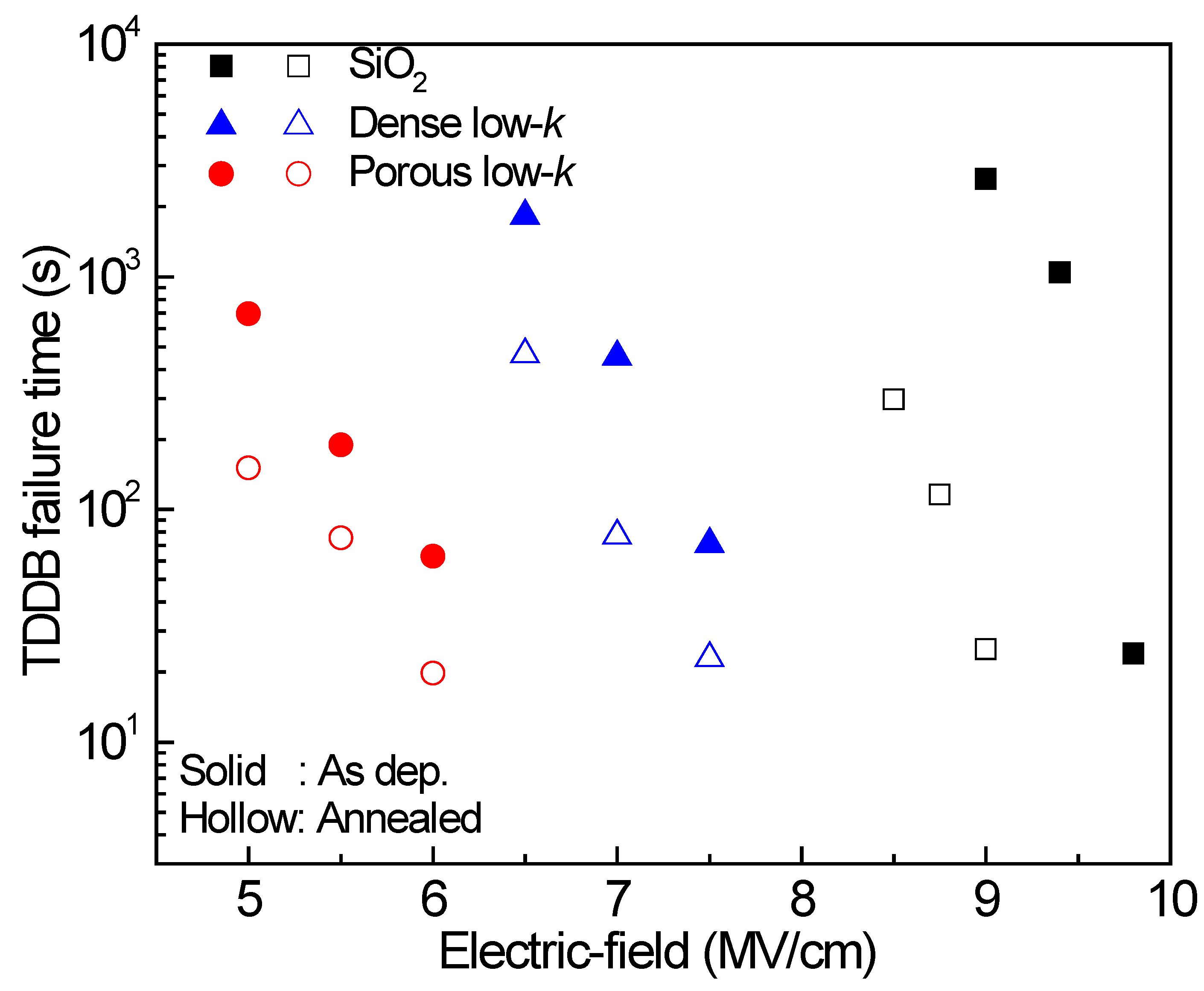
Figure 7.
Changes in the electric-field acceleration factor for SiO2, dense, and porous low-k dielectric films in Co-gate MIS capacitors after annealing.
Figure 7.
Changes in the electric-field acceleration factor for SiO2, dense, and porous low-k dielectric films in Co-gate MIS capacitors after annealing.
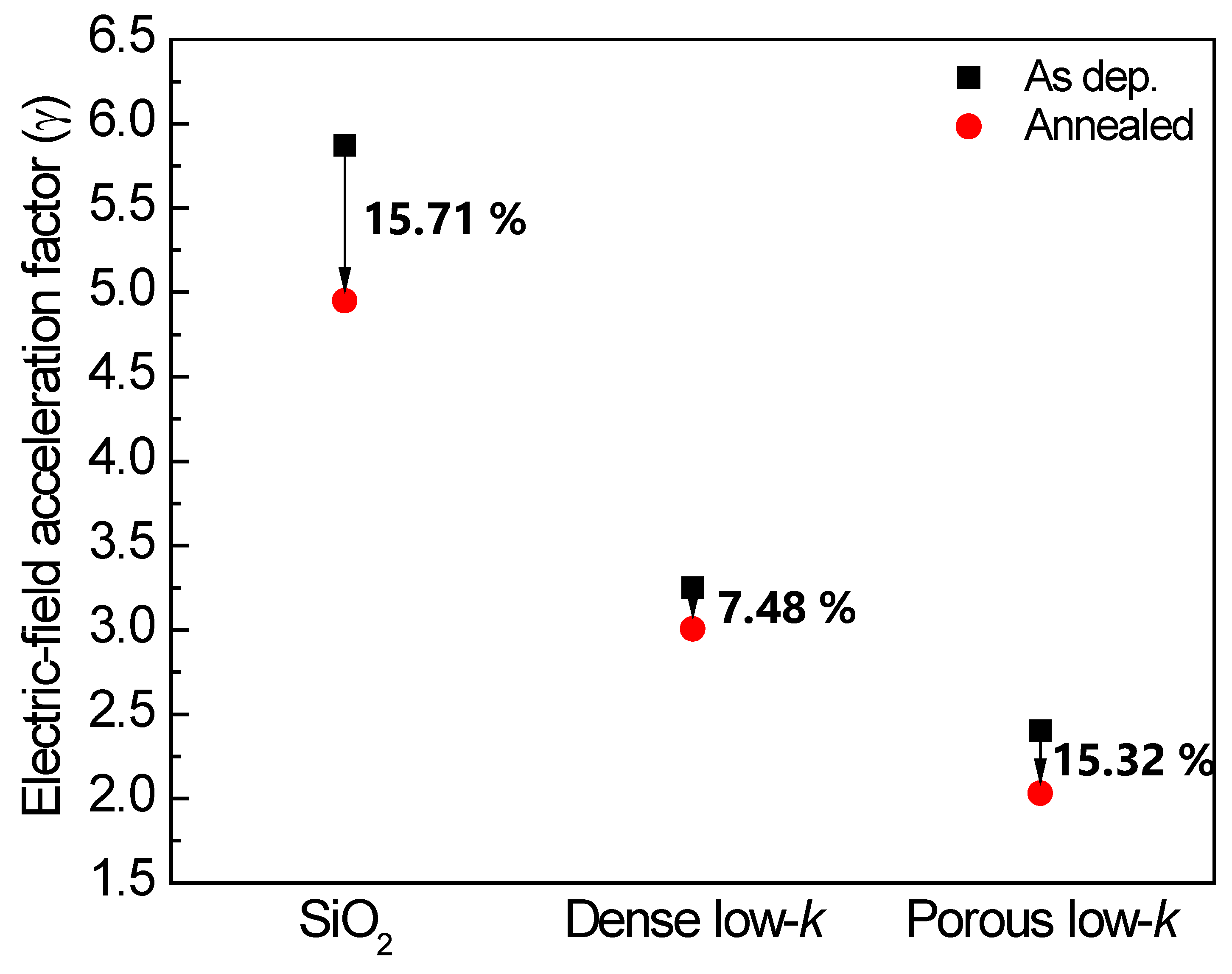
Figure 8.
I–E plots of Co-gate MIS capacitors with porous low-k films before and after positive-polarity electrical stress with various fields.
Figure 8.
I–E plots of Co-gate MIS capacitors with porous low-k films before and after positive-polarity electrical stress with various fields.
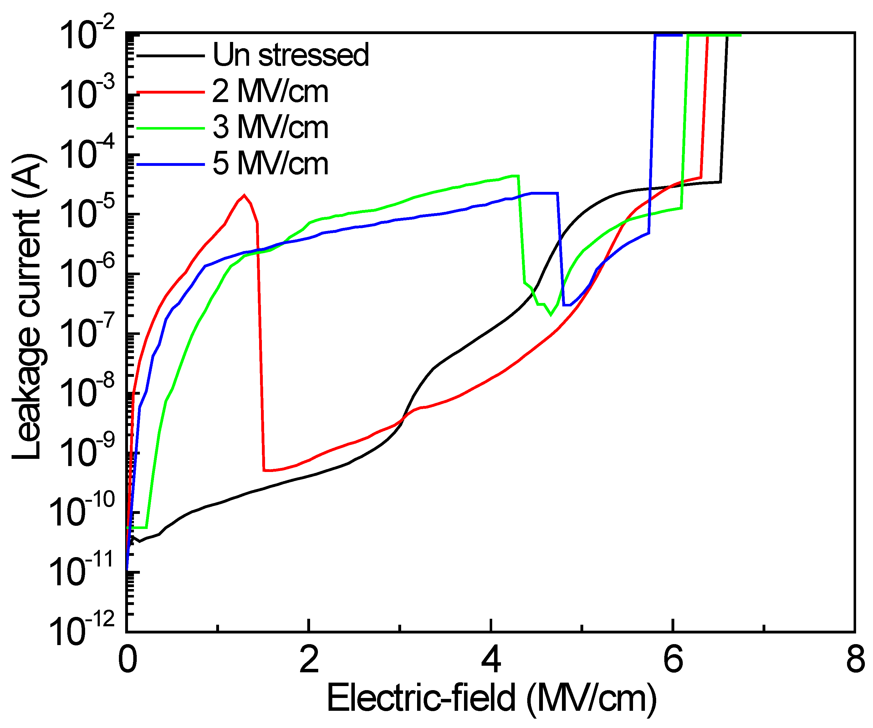
Figure 9.
Reduction of the breakdown field for SiO2, dense, and porous low-k dielectric films in Co-gate MIS capacitors after being subjected to positive-polarity electrical stress as a function of the stressing electric field.
Figure 9.
Reduction of the breakdown field for SiO2, dense, and porous low-k dielectric films in Co-gate MIS capacitors after being subjected to positive-polarity electrical stress as a function of the stressing electric field.

Table 1.
Properties of SiO2, dense, and porous low-k dielectric films ued in this study.
| Sample | Deposition Method | Precursor | UV Curing | Dielectric Constant (k) | Leakage Current Density at 1 MV/cm (×10−12A/cm2) | Breakdown Filed at 25 °C (MV/cm) | Porosity (%) | Pore Size (nm) |
|---|---|---|---|---|---|---|---|---|
| SiO2 | Dry oxidation | O2 | No | 4.02 ± 0.03 | 2.46 ± 0.35 | 9.98 ± 0.15 | N/D | N/D |
| Dense low-k | PECVD | DEMS + O2 | No | 3.02 ± 0.05 | 5.66 ± 0.7 | 8.56 ±0.16 | N/D | N/D |
| Porous low-k | PECVD | DEMS + O2 + ATRP | Yes | 2.56 ± 0.08 | 2.69 ± 0.33 | 6.67 ± 0.30 | 15 | 1.35 |
N/D = not detected.
Disclaimer/Publisher’s Note: The statements, opinions and data contained in all publications are solely those of the individual author(s) and contributor(s) and not of MDPI and/or the editor(s). MDPI and/or the editor(s) disclaim responsibility for any injury to people or property resulting from any ideas, methods, instructions or products referred to in the content. |
© 2023 by the authors. Licensee MDPI, Basel, Switzerland. This article is an open access article distributed under the terms and conditions of the Creative Commons Attribution (CC BY) license (https://creativecommons.org/licenses/by/4.0/).
Share and Cite
MDPI and ACS Style
Cheng, Y.-L.; Huang, H.-C.; Peng, W.-F.; Chen, G.-S.; Fang, J.-S. Comparison of Cobalt Integration with Various Dielectric Materials under Thermal and Electrical Stress. Coatings 2023, 13, 1818. https://doi.org/10.3390/coatings13101818
AMA Style
Cheng Y-L, Huang H-C, Peng W-F, Chen G-S, Fang J-S. Comparison of Cobalt Integration with Various Dielectric Materials under Thermal and Electrical Stress. Coatings. 2023; 13(10):1818. https://doi.org/10.3390/coatings13101818
Chicago/Turabian StyleCheng, Yi-Lung, Hong-Chang Huang, Wei-Fan Peng, Giin-Shan Chen, and Jau-Shiung Fang. 2023. "Comparison of Cobalt Integration with Various Dielectric Materials under Thermal and Electrical Stress" Coatings 13, no. 10: 1818. https://doi.org/10.3390/coatings13101818
Note that from the first issue of 2016, this journal uses article numbers instead of page numbers. See further details here.