
Collision Cascade in a Silicon-Based Device under Energetic Ar Ions Irradiation

Abstract
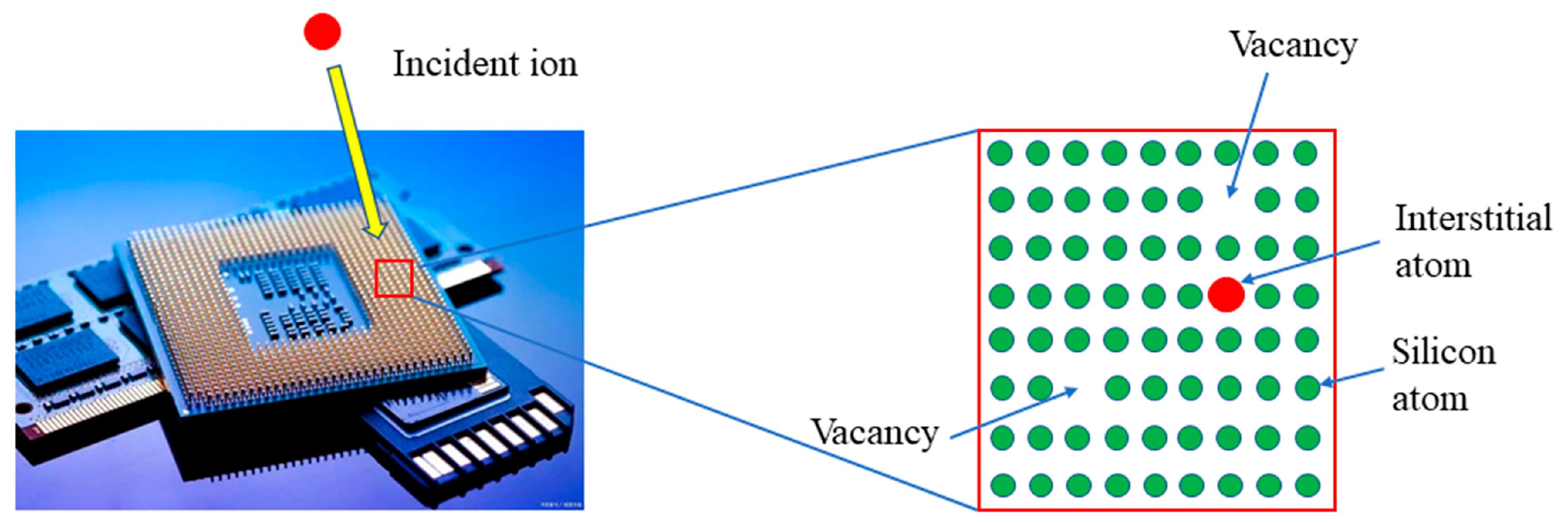
:1. Introduction
2. Modelling and Methods
2.1. Monte Carlo Simulation
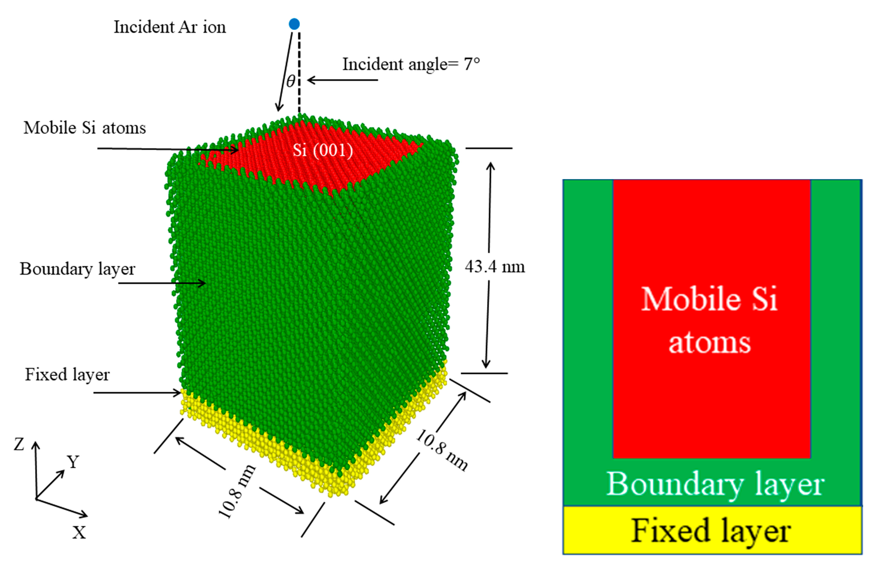
2.2. Molecular Dynamics Simulation
3. Results and Discussion
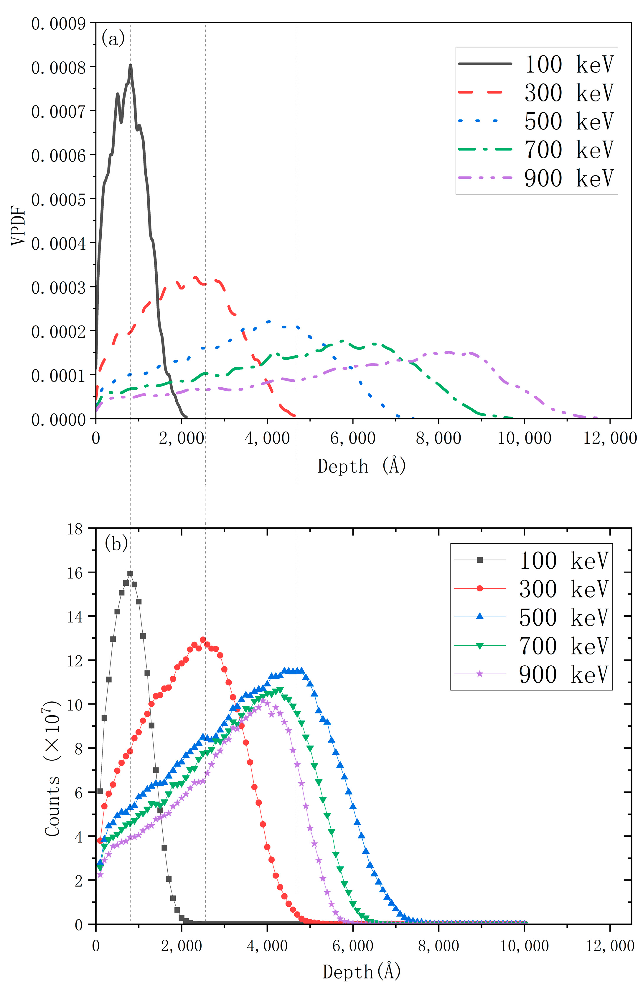
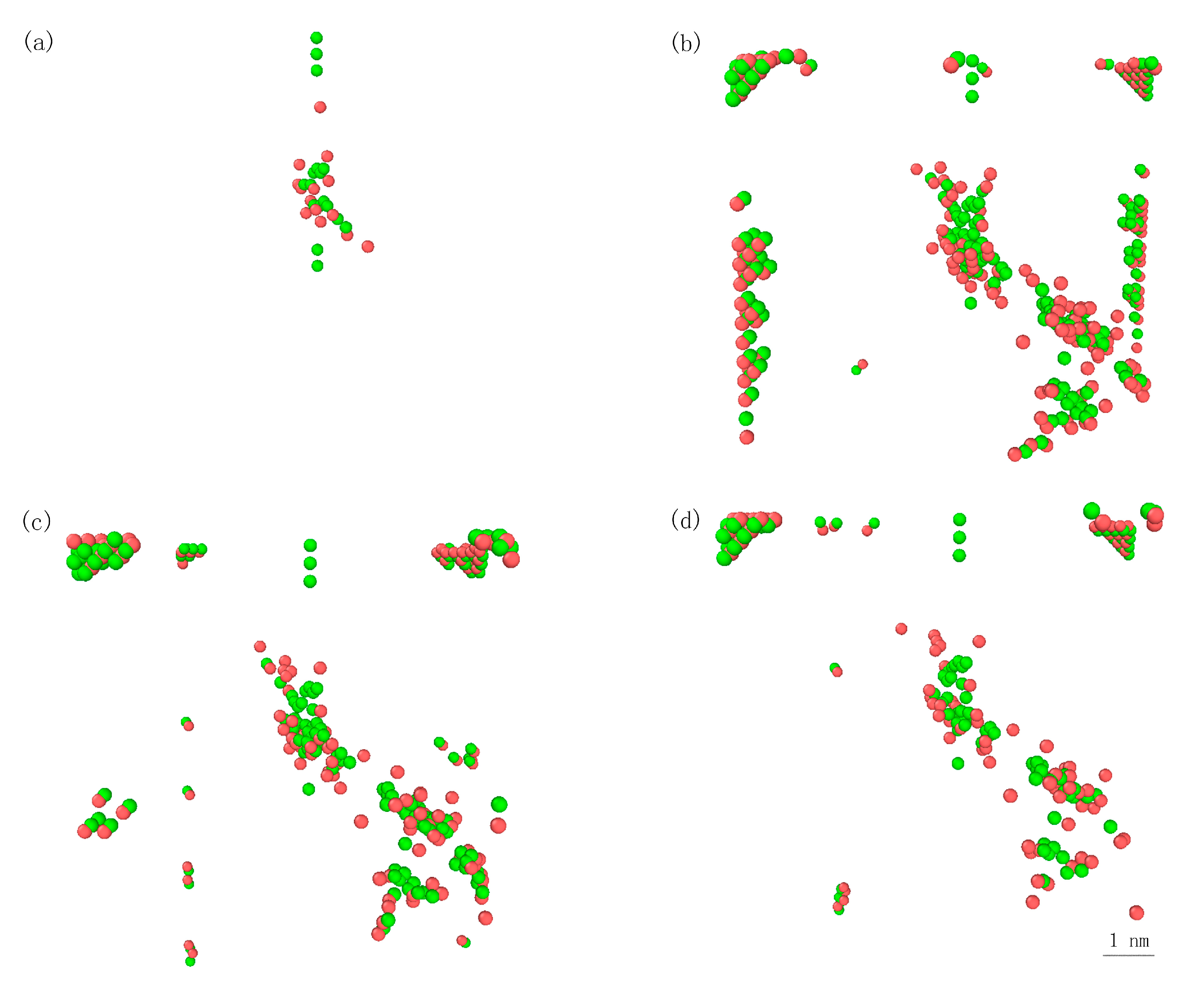
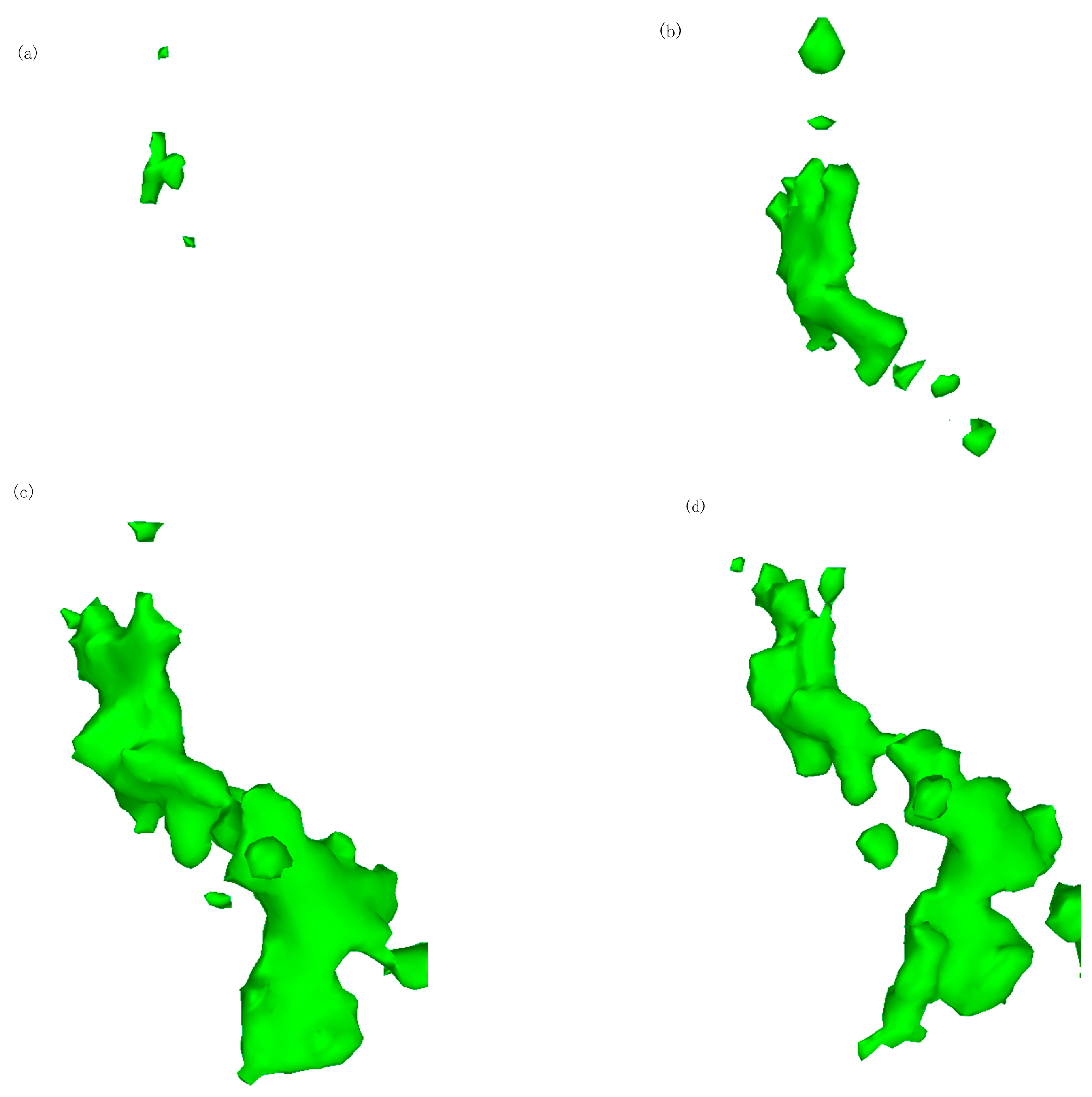
3.1. Vacancy Probability Density
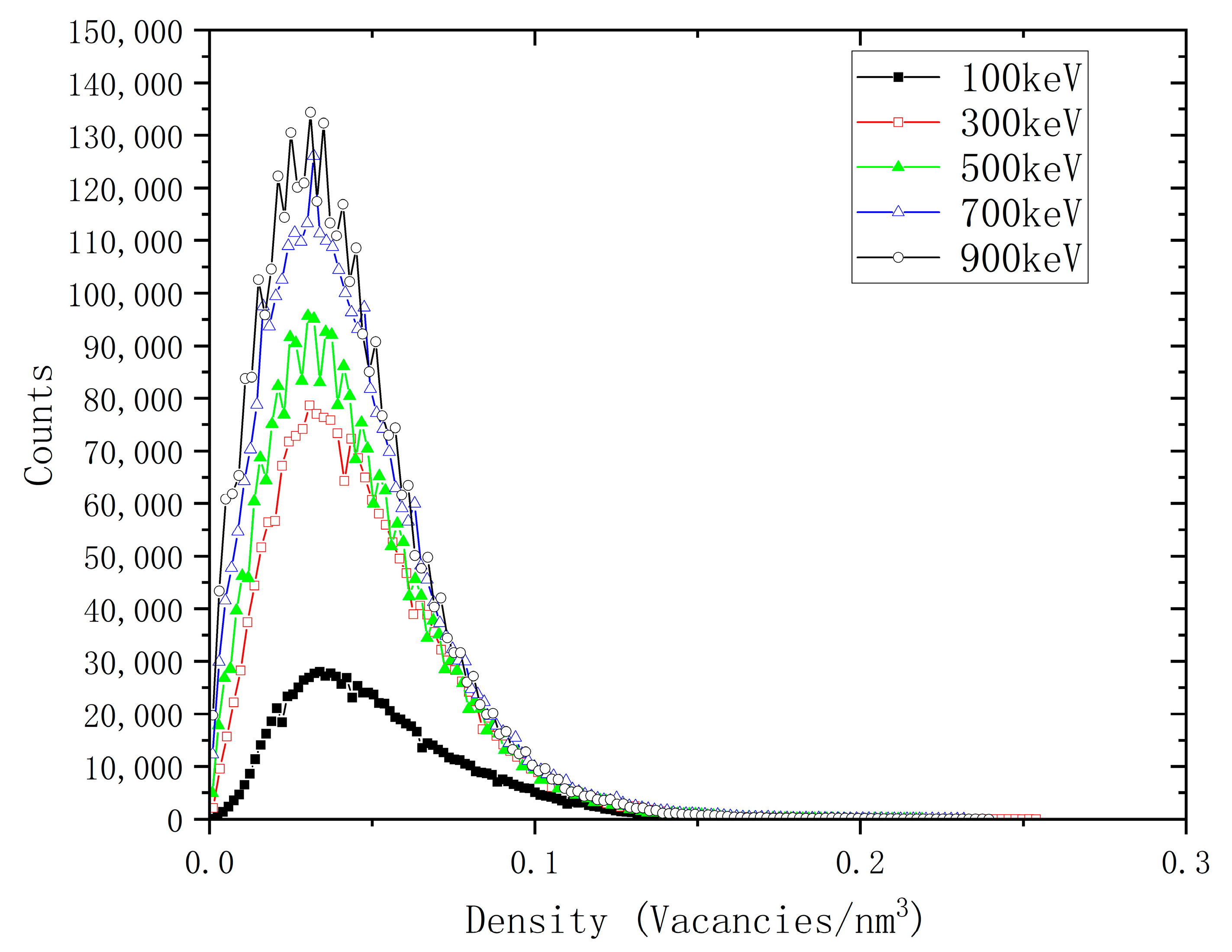
3.2. Local Collision Cascade Density
3.3. Ionization Energy Loss
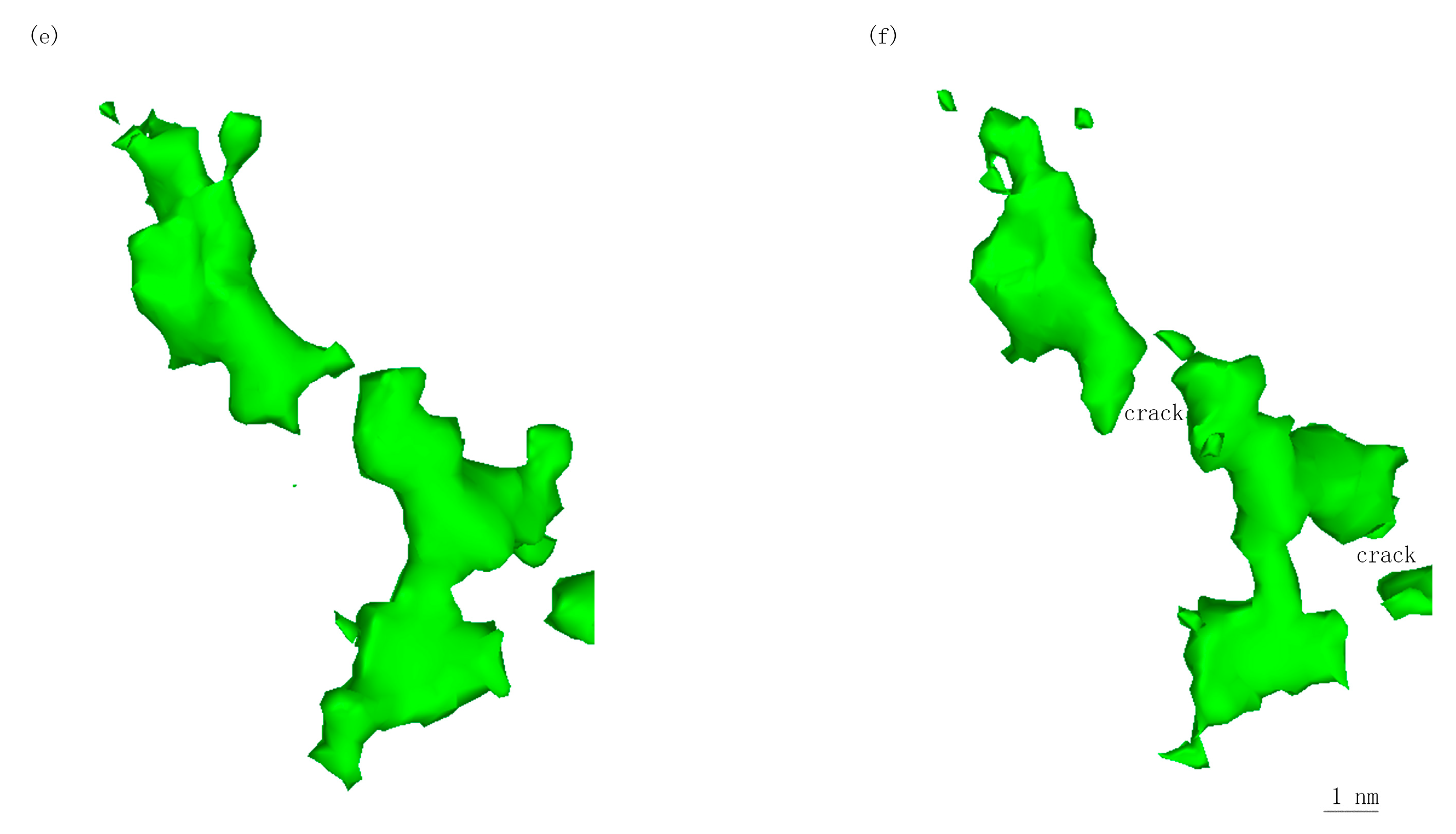
3.4. Defect Evolution
4. Conclusions
Author Contributions
Funding
Institutional Review Board Statement
Informed Consent Statement
Data Availability Statement
Acknowledgments
Conflicts of Interest
References
- Leroy, C.; Rancoita, P.G. Particle Interaction and Displacement Damage in Silicon Devices Operated in Radiation Environments. Rep. Prog. Phys. 2007, 70, 493–625. [Google Scholar] [CrossRef]
- Aji, L.B.B.; Wallace, J.B.; Kucheyev, S.O. Effects of Collision Cascade Density on Radiation Defect Dynamics in 3C-SiC. Sci. Rep. 2017, 7, 44703. [Google Scholar] [CrossRef]
- Wallace, J.B.; Aji, L.B.B.; Martin, A.A.; Shin, S.J.; Shao, L.; Kucheyev, S.O. The Role of Frenkel Defect Diffusion in Dynamic Annealing in Ion-Irradiated Si. Sci. Rep. 2017, 7, 39754. [Google Scholar] [CrossRef]
- Bayu Aji, L.B.; Wallace, J.B.; Shao, L.; Kucheyev, S.O. Non-Monotonic Temperature Dependence of Radiation Defect Dynamics in Silicon Carbide. Sci. Rep. 2016, 6, 30931. [Google Scholar] [CrossRef] [PubMed]
- Wallace, J.B.; Charnvanichborikarn, S.; Bayu Aji, L.B.; Myers, M.T.; Shao, L.; Kucheyev, S.O. Radiation Defect Dynamics in Si at Room Temperature Studied by Pulsed Ion Beams. J. Appl. Phys. 2015, 118, 135709. [Google Scholar] [CrossRef]
- Azarov, A.Y.; Titov, A.I.; Karaseov, P.A.; Hallén, A. Effect of Collision Cascade Density on Radiation Damage in SiC. Nucl. Instrum. Methods Phys. Res. Sect. B Beam Interact. Mater. Atoms 2009, 267, 1247–1250. [Google Scholar] [CrossRef]
- Pelenitsyn, V.; Korotaev, P. First-Principles Study of Radiation Defects in Silicon. Comput. Mater. Sci. 2022, 207, 111273. [Google Scholar] [CrossRef]
- Mihai, M.D.; Iancu, D.; Zarkadoula, E.; Florin, R.A.; Tong, Y.; Zhang, Y.; Weber, W.J.; Velişa, G. Athermal Annealing of Pre-Existing Defects in Crystalline Silicon. Acta Mater. 2023, 261, 119379. [Google Scholar] [CrossRef]
- Al-Sharif, A.; AlAderah, B.; Obeidat, A.; Talla, J. Influence of Transition Metal Defects on Electronic and Magnetic Properties of Bulk Silicon: Ab-Initio Simulation. Mater. Today Commun. 2023, 34, 105415. [Google Scholar] [CrossRef]
- Cherkova, S.G.; Volodin, V.A.; Skuratov, V.A.; Stoffel, M.; Rinnert, H.; Vergnat, M. Formation of Light-Emitting Defects in Silicon by Swift Heavy Ion Irradiation and Subsequent Annealing. Nucl. Instrum. Methods Phys. Res. Sect. B Beam Interact. Mater. Atoms 2023, 535, 132–136. [Google Scholar] [CrossRef]
- Huang, N.; Zhou, P.; Goel, S. Microscopic Stress Analysis of Nanoscratch Induced Sub-Surface Defects in a Single-Crystal Silicon Wafer. Precis. Eng. 2023, 82, 290–303. [Google Scholar] [CrossRef]
- Tang, S.; Qi, X.; Chang, C.; Wang, Q.; Liu, L. Reduction of the Initial Defects Generated during Casting of Quasi-Single Crystalline Silicon by Reserving Gaps between Seed Crystals. Sol. Energy Mater. Sol. Cells 2023, 263, 112571. [Google Scholar] [CrossRef]
- Li, Q.; Lin, X.; Lin, X.H.; Xing, Y.; Zhou, Z. Experimental Study on the Thermal Evolution of Silicon Defects with Zonal Characteristics Induced by Precisely Localized Irradiation of Focused Helium Ion Beams. Vacuum 2023, 218, 112615. [Google Scholar] [CrossRef]
- Fan, Y.; Xu, Z.; Song, Y.; Sun, T. Molecular Dynamics Simulation of Silicon Vacancy Defects in Silicon Carbide by Hydrogen Ion Implantation and Subsequent Annealing. Diam. Relat. Mater. 2021, 119, 108595. [Google Scholar] [CrossRef]
- Nordlund, K. Historical Review of Computer Simulation of Radiation Effects in Materials. J. Nucl. Mater. 2019, 520, 273–295. [Google Scholar] [CrossRef]
- Vaitkus, J.V.; Rumbauskas, V.; Mockevicius, G.; Zasinas, E.; Mekys, A. An Evidence of Strong Electron-Phonon Interaction in the Neutron Irradiation Induced Defects in Silicon. Nucl. Instrum. Methods Phys. Res. Sect. A Accel. Spectrometers Detect. Assoc. Equip. 2015, 796, 114–117. [Google Scholar] [CrossRef]
- Starinskiy, S.V.; Rodionov, A.A.; Shukhov, Y.G.; Safonov, A.I.; Maximovskiy, E.A.; Sulyaeva, V.S.; Bulgakov, A.V. Formation of Periodic Superhydrophilic Microstructures by Infrared Nanosecond Laser Processing of Single-Crystal Silicon. Appl. Surf. Sci. 2020, 512, 145753. [Google Scholar] [CrossRef]
- Evseev, A.P.; Kozhemiako, A.V.; Kargina, Y.V.; Balakshin, Y.V.; Zvereva, E.A.; Chernysh, V.S.; Gongalsky, M.B.; Shemukhin, A.A. Radiation-Induced Paramagnetic Defects in Porous Silicon under He and Ar Ion Irradiation. Radiat. Phys. Chem. 2020, 176, 109061. [Google Scholar] [CrossRef]
- Shen, J.; Yu, X.; Zhang, Y.; Zhong, H.; Zhang, J.; Qu, M.; Yan, S.; Zhang, G.; Zhang, X.; Le, X. Novel Microstructures on the Surfaces of Single Crystal Silicon Irradiated by Intense Pulsed Ion Beams. Nucl. Instrum. Methods Phys. Res. Sect. B Beam Interact. Mater. Atoms 2015, 365, 26–29. [Google Scholar] [CrossRef]
- Shen, J.; Shahid, I.; Yu, X.; Zhang, J.; Zhong, H.; Cui, X.; Liang, G.; Yu, X.; Huang, W.; Yan, S.; et al. Fracture Analysis of Surface Exfoliation on Single Crystal Silicon Irradiated by Intense Pulsed Ion Beam. Nucl. Instrum. Methods Phys. Res. Sect. B Beam Interact. Mater. Atoms 2017, 413, 6–12. [Google Scholar] [CrossRef]
- Shen, J.; Shahid, I.; Yu, X.; Zhang, J.; Zhong, H.W.; Yu, X.; Huang, W.Y.; Liang, G.Y.; Cui, X.J.; Yan, S.; et al. Surface Exfoliation Analysis on Single-Crystal Silicon under Compressed Plasma Flow Action. Laser Part. Beams 2018, 36, 129–135. [Google Scholar] [CrossRef]
- Liang, G.; Zhong, H.; Zhang, S.; Xu, M.; Kuang, S.; Ren, J.; Zhang, N.; Yan, S.; Yu, X.; Remnev, G.E.; et al. Molecular Dynamics Study of Damage Nearby Silicon Surface Bombarded by Energetic Carbon Ions. Surf. Coat. Technol. 2020, 385, 125350. [Google Scholar] [CrossRef]
- Liang, G.; Zhong, H.; Wang, Y.; Zhang, S.; Xu, M.; Kuang, S.; Ren, J.; Zhang, N.; Yan, S.; Yu, X.; et al. Molecular Dynamics Simulations of Vacancy Generation and Migration near a Monocrystalline Silicon Surface during Energetic Cluster Ion Implantation. Coatings 2020, 10, 146. [Google Scholar] [CrossRef]
- Wallace, J.B.; Aji, L.B.B.; Shao, L.; Kucheyev, S.O. Fractal Analysis of Collision Cascades in Pulsed-Ion-Beam-Irradiated Solids. Sci. Rep. 2017, 7, 17574. [Google Scholar] [CrossRef] [PubMed]
- Wallace, J.B.; Aji, L.B.B.; Shao, L.; Kucheyev, S.O. Deterministic Role of Collision Cascade Density in Radiation Defect Dynamics in Si. Phys. Rev. Lett. 2018, 120, 216101. [Google Scholar] [CrossRef]
- Bayu Aji, L.B.; Wallace, J.; Kucheyev, S. Radiation Defect Dynamics in 3C-, 4H-, and 6H-SiC Studied by Pulsed Ion Beams. Nucl. Instrum. Methods Phys. Res. Sect. B Beam Interact. Mater. Atoms 2018, 435, 8–11. [Google Scholar] [CrossRef]
- Myers, M.T.; Charnvanichborikarn, S.; Shao, L.; Kucheyev, S.O. Pulsed Ion Beam Measurement of the Time Constant of Dynamic Annealing in Si. Phys. Rev. Lett. 2012, 109, 2–5. [Google Scholar] [CrossRef]
- Ziegler, J.F.; Ziegler, M.D.; Biersack, J.P. SRIM—The Stopping and Range of Ions in Matter (2010). Nucl. Instrum. Methods Phys. Res. Sect. B Beam Interact. Mater. Atoms 2010, 268, 1818–1823. [Google Scholar] [CrossRef]
- Plimpton, S. Fast Parallel Algorithms for Short-Range Molecular Dynamics. J. Comput. Phys. 1995, 117, 1–19. [Google Scholar] [CrossRef]
- Ziegler, J.; Biersack, J.; Littmark, U. The Stopping and Range of Ions in Solids; Pergamon Press: New York, NY, USA, 1985. [Google Scholar]
- Tersoff, J. Modeling Solid-State Chemistry: Interatomic Potentials for Multicomponent Systems. Phys. Rev. B 1989, 39, 5566–5568. [Google Scholar] [CrossRef]
- Xiao, Y.J.; Fang, F.Z.; Xu, Z.W.; Hu, X.T. Annealing Recovery of Nanoscale Silicon Surface Damage Caused by Ga Focused Ion Beam. Appl. Surf. Sci. 2015, 343, 56–69. [Google Scholar] [CrossRef]
- Stukowski, A. Visualization and Analysis of Atomistic Simulation Data with OVITO-the Open Visualization Tool. Model. Simul. Mater. Sci. Eng. 2010, 18, 015012. [Google Scholar] [CrossRef]
- Bai, X.M.; Voter, A.F.; Hoagland, R.G.; Nastasi, M.; Uberuaga, B.P. Efficient Annealing of Radiation Damage near Grain Boundaries via Interstitial Emission. Science 2010, 327, 1631–1634. [Google Scholar] [CrossRef] [PubMed]


| Incident Ions (keV) | Recoil Atoms (keV) | |||||||||
|---|---|---|---|---|---|---|---|---|---|---|
| 100 | 300 | 500 | 700 | 900 | 100 | 300 | 500 | 700 | 900 | |
| Ionization | 30.99% | 47.83% | 56.38% | 62.16% | 66.97% | 28.02% | 23.59% | 20.58% | 18.32% | 16.14% |
| Vacancies | 0.17% | 0.10% | 0.08% | 0.07% | 0.06% | 3.23% | 2.26% | 1.82% | 1.54% | 1.33% |
| Phonons | 0.52% | 0.33% | 0.27% | 0.24% | 0.22% | 37.08% | 25.88% | 20.87% | 17.67% | 15.28% |
Disclaimer/Publisher’s Note: The statements, opinions and data contained in all publications are solely those of the individual author(s) and contributor(s) and not of MDPI and/or the editor(s). MDPI and/or the editor(s) disclaim responsibility for any injury to people or property resulting from any ideas, methods, instructions or products referred to in the content. |
© 2023 by the authors. Licensee MDPI, Basel, Switzerland. This article is an open access article distributed under the terms and conditions of the Creative Commons Attribution (CC BY) license (https://creativecommons.org/licenses/by/4.0/).
Share and Cite
Liang, G.; Xu, B.; Wei, X. Collision Cascade in a Silicon-Based Device under Energetic Ar Ions Irradiation. Coatings 2023, 13, 1828. https://doi.org/10.3390/coatings13111828
Liang G, Xu B, Wei X. Collision Cascade in a Silicon-Based Device under Energetic Ar Ions Irradiation. Coatings. 2023; 13(11):1828. https://doi.org/10.3390/coatings13111828
Chicago/Turabian StyleLiang, Guoying, Baoming Xu, and Xiaoyun Wei. 2023. "Collision Cascade in a Silicon-Based Device under Energetic Ar Ions Irradiation" Coatings 13, no. 11: 1828. https://doi.org/10.3390/coatings13111828