Article

Effect of Titanium Cation Doping on the Performance of In2O3 Thin Film Transistors Grown via Atomic Layer Deposition

1
Key Laboratory of Advanced Display and System Application, Ministry of Education, Shanghai University, Shanghai 200072, China
2
School of Microelectronics, Shanghai University, Shanghai 200072, China
3
School of Mechatronics and Automation, Shanghai University, Shanghai 200072, China
4
Huzhou Key Laboratory of Medical and Environmental Applications Technologies, School of Life Sciences, Huzhou University, Huzhou 313000, China
*
Authors to whom correspondence should be addressed.
Coatings 2023, 13(3), 605; https://doi.org/10.3390/coatings13030605
Submission received: 4 February 2023 / Revised: 7 March 2023 / Accepted: 10 March 2023 / Published: 12 March 2023
(This article belongs to the Special Issue Advanced Films and Coatings Based on Atomic Layer Deposition)

Abstract

:
Indium oxide semiconductors, as one of the channel materials for thin film transistors (TFTs), have been extensively studied. However, the high carrier concentration and excess oxygen defects of intrinsic In2O3 can cause the devices to fail to work properly. We overcame this hurdle by incorporating the titanium cation (Ti4+) into In2O3 via atomic layer deposition (ALD). The InTiOx TFTs with an In:Ti atomic ratio of 15:1 demonstrated excellent electrical and optical properties, such as a lower threshold voltage (Vth) of 0.17 V, a lower subthreshold swing (SS) of 0.13 V/dec., a higher Ion/Ioff ratio of 107, and a transmittance greater than 90% in the visible region. With the doping ratio increasing from 20:1 to 10:1, the mobility decreased from 9.38 to 1.26 cm2/Vs. The threshold voltage shift (ΔVth) of InTiO (15:1) under 5 V positive bias stress (PBS) for 900 s is 0.93 V, which is less than other devices. The improvement in stability with increasing Ti4+ concentrations is attributed to the reduction of oxygen defects. Therefore, these InTiO (15:1) TFTs with excellent performance show great potential for future applications in transparent electronic devices.

1. Introduction

Recently, amorphous oxide semiconductors (AOS) have received extensive attention in the field of flat panel displays and wearable devices due to their excellent photoelectric properties [1,2,3]. Among the various candidate materials, indium oxide (In2O3) with a wide bandgap (3.6–3.7 eV) has a high transmittance to visible light and exhibits excellent chemical stability [4,5,6], making it one of the most promising thin film transistor channel materials. In-ions with an outer electronic structure of (n − 1)d10ns0 (n ≥ 4) [7] contribute greatly to increasing the carrier concentration and mobility of in-based TFTs. However, its practical application is limited by the instability of In2O3 TFTs due to excessive oxygen vacancies (VO). Therefore, it is essential for large-scale applications to perfect the stability of In2O3 TFTs. To date, several doping elements have been reported to improve the stability of devices, including Al [8], Ga [9], and Mg [10], which could suppress the formation of VO. To obtain stable indium oxide TFTs, the doping element and oxygen should have a higher bond dissociation energy than In-O (360 kJ/mol). Among the many doping elements, titanium (Ti-O) has a larger oxygen bonding dissociation energy (662 kJ/mol) [6] than indium (In-O), which can reduce the VO concentration in the In2O3 film and be an effective oxygen vacancy inhibitor.
Among the methods for depositing oxide thin films, magnetron sputtering [11], electrospinning [12], sol-gel [13], etc. are not satisfactory in terms of uniformity of film formation and control of film thickness. Atomic layer deposition (ALD) technology offers many advantages over the above preparation methods, including excellent repeatability, low deposition temperatures, and high control of composition and thickness [14,15,16]. As a result of the self-limiting nature of the ALD process, thin oxide films with precise thickness and conformability can be formed. For instance, Bak et al. [17] prepared IZTO TFTs with high-k HfO2 as the dielectric layer by atomic layer deposition. Compared with HfO2 dielectric devices prepared by magnetron sputtering, IZTO TFT samples prepared by the ALD method have a higher Ion/Ioff ratio and slightly improved field effect mobility. Yang et al. [18] fabricated 5 nm ultrathin ZrO2 dielectrics by ALD for high-performance ZnO TFTs. The TFTs exhibit the lowest operating voltage of 1 V, field effect mobility of 36.8 cm2/Vs, and SS of 69 mV/dec., which is close to the theoretical limit. Sheng et al. [19] successfully fabricated IGZO TFTs by PEALD with mobility up to 70 cm2/Vs. As shown above, ALD processes have the potential to fabricate oxide TFTs with many advantages.
In this work, InTiO TFTs were fabricated using the ALD technique. Through the application of the proper amount of Ti4+ doping, we have demonstrated improved electrical performance and stability of InTiO TFTs due to a reduction in VO defects and the density of interface traps.

2. Experiments

Figure 1a shows TFT fabricated on a 0.45-mm-thick p-type silicon wafer substrate with a bottom gate and top contact. Prior to preparation, the silicon substrates were washed sequentially with acetone, alcohol, and deionized water for 15 min in a sonicator, followed by 10 min of ozone and ultraviolet light treatment to enhance hydrophilicity. Subsequently, the 50-nm Al2O3 dielectric was deposited by the thermal ALD (TFS-200, Beneq) method at 250 °C with trimethylaluminum (TMA) and deionized water as aluminum and oxygen precursors, respectively. The optimized ALD cycle consists of a 200-ms precursor pulse combined with a 10-s N2 purge. The InTiO films were grown on Al2O3 for the active layer at a growth temperature of 200 °C. High-purity (3-dimethylaminopropyl) dimethylindium (DADI) and tetrakis (dimethylamino) titanium (TDMATi) were used as precursors for indium and titanium, respectively, and ozone and deionized water were used as oxygen sources. The DADI and TDMATi canisters were heated to 35 and 45 °C, respectively. The pulse times of DADI and O3 were 200/300 ms, and the pulse times of TDMATi and H2O were 500/250 ms. The nitrogen purging time is 5 s. X cycles of DADI/O3 followed by one cycle of TDMATi/H2O were repeated for Ti4+ incorporation into the In2O3 film, where X varied between 20, 18, 15, and 10, and films with approximately 17 nm thickness were obtained by adjusting the total supercycles. Thus, the grown InTiO thin films with different In2O3 sublayer cycles are named from InTiO (20:1) to InTiO (10:1). Figure 1b presents the detailed growth conditions, and Figure 1c shows the cross-sectional TEM image of the InTiO TFT. The pure In2O3 film was also prepared by ALD for contrastive analysis. After the active layer was deposited, 200-nm Al films were deposited by thermal evaporation as the source/drain electrodes. The channel width (W) and channel length (L) were 1000 and 100 µm, respectively. The devices were then annealed in the air for 10 min at 250 °C. The same process was used to grow InTiO thin films on quartz glass substrates to investigate their optical properties.
Through X-ray diffraction (XRD; Rigaku D/max-rB, Akishima, Japan) and X-ray photoelectron spectroscopy (XPS; Thermo Scientific K-Alpha+, Waltham, MA, USA), the crystal structure and chemical composition of the thin films were characterized. Atomic force microscopy (AFM, nanonaviSPA-400 SPM, SII Nano Technology Inc. Chiba City, Japan) was used to observe surface morphology, and a double-beam spectrophotometer (Hitachi U-3900H, Tokyo, Japan) was used to measure optical transmission. The semiconductor characteristics of TFT were measured by a semiconductor parameter analyzer (Keithley, 4200, Cleveland, OH, USA) and probe station (Lakeshore, TTP4, Carson, CA, USA). The electrical properties were tested by the Hall effect (Lakeshore 8400, Toyo Corporation, Tokyo, Japan).

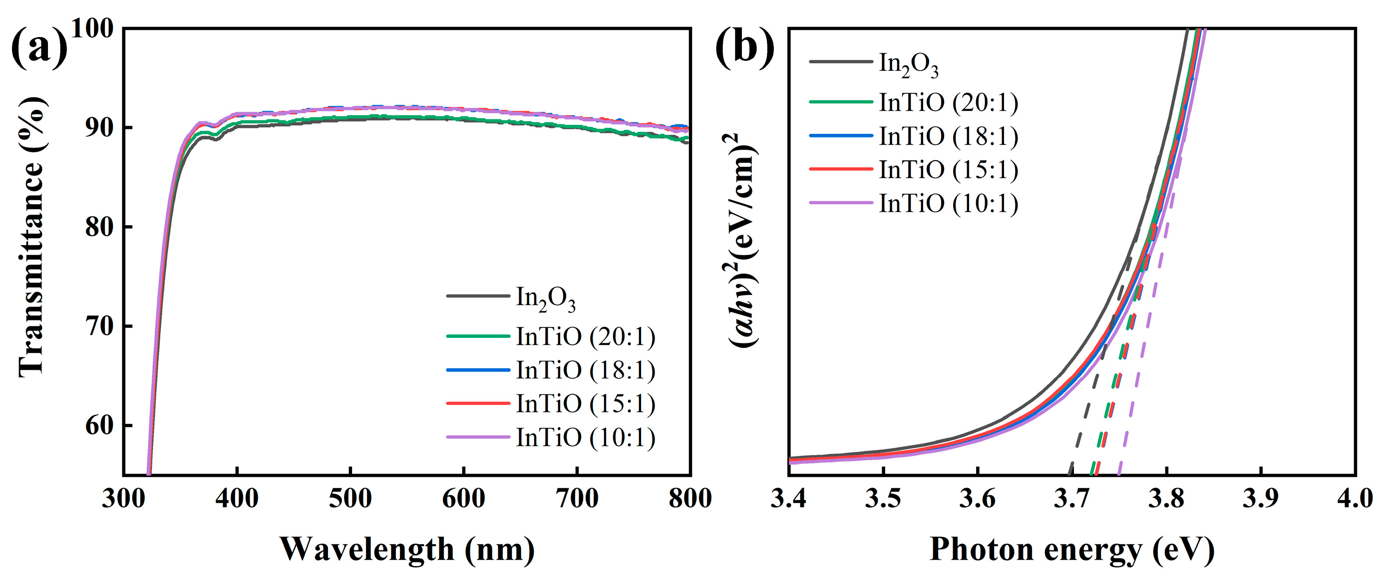
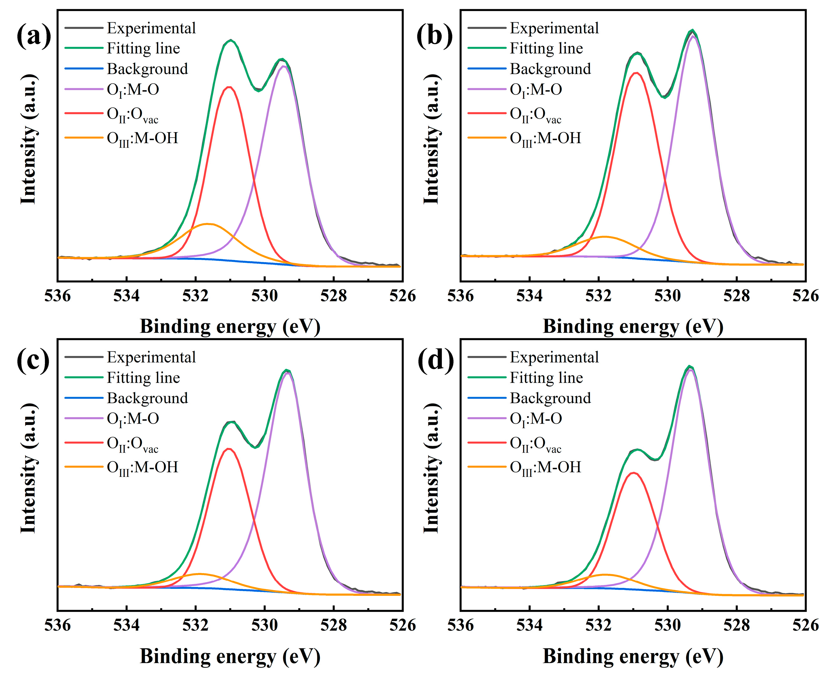
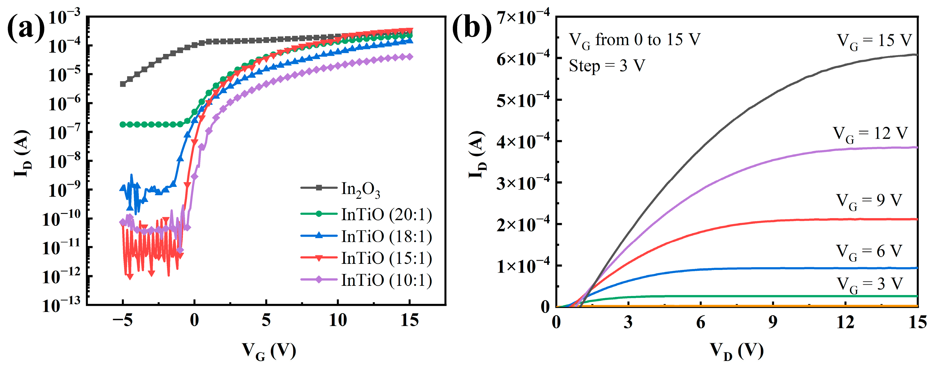
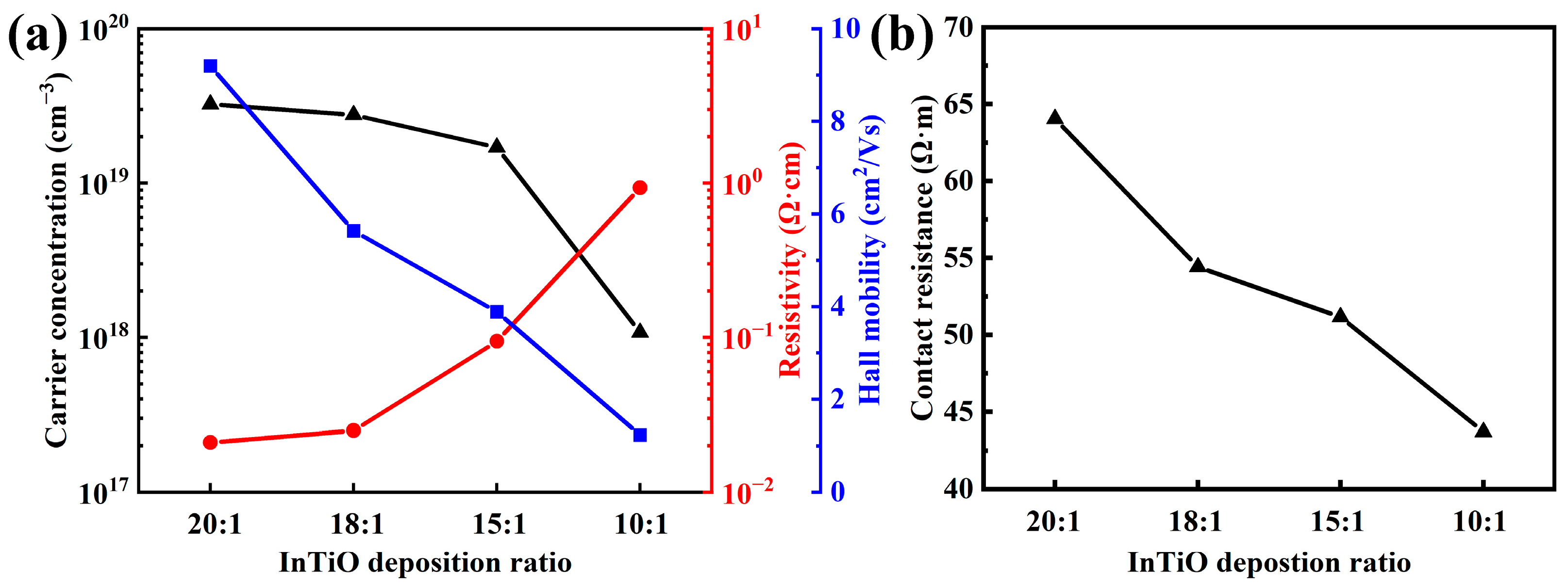
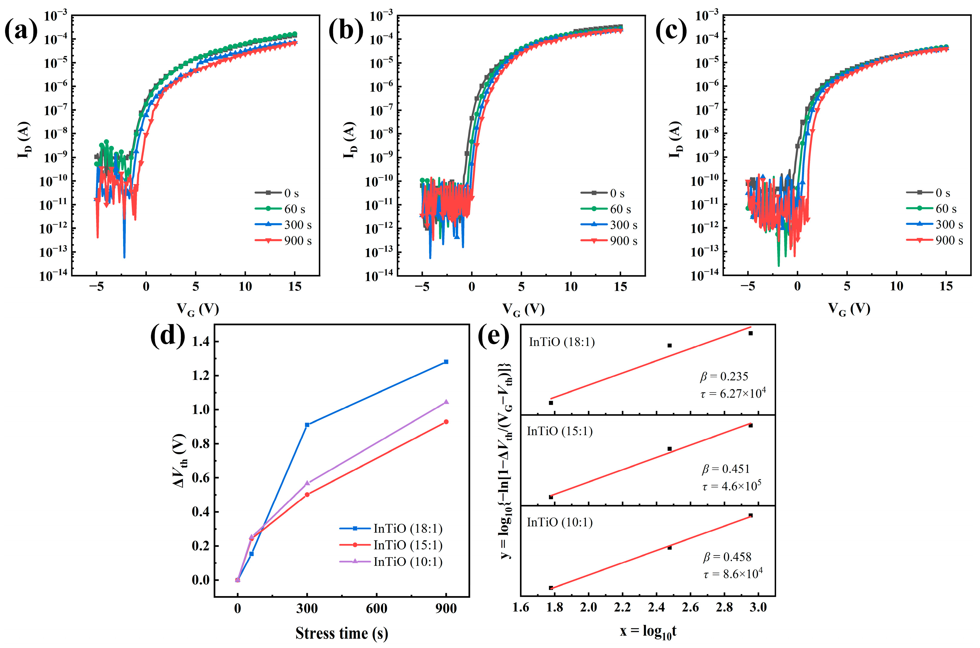
3. Results and Discussion

To evaluate the morphological evolution of the films with different composition ratios, the resulting InTiO films were characterized by AFM in the region of 2 µm × 2 µm, as shown in Figure 2a–d. AFM micrographs show a systematic decrease in surface roughness with decreasing number of X cycles (higher Ti4+ doping ratio), which is well displayed by the obtained root mean squared (RMS) values due to the decrease in crystallinity of the film caused by Ti4+ implantation. The values of RMS for InTiO (20:1), InTiO (18:1), InTiO (15:1), and InTiO (10:1) are 0.32, 0.28, 0.27, and 0.26 nm, respectively. The roughness of the active layer is one of the important parameters for ensuring high-performance thin-film transistor devices [20]. Its smooth surface is beneficial to source and drain electrode adhesion [21], thereby reducing the contact resistance between the electrode and the active layer. Contact resistance will be discussed later. All InTiO films have very flat surface morphology, which will help to reduce carrier scattering and promote mobility. Amorphous structures are observed in the XRD patterns of InTiO thin films, as shown in Figure 2e. TFT devices can be manufactured with high uniformity and smooth surfaces thanks to the amorphous phase [22]. The results are consistent with AFM analysis.
The optical transmission spectra of all films on quartz glass substrates were measured in order to determine the effect of different Ti4+ doping ratios on the optical band gap (Eg) of films. As shown in Figure 3a, all samples in the visible range have a transmittance of about 90%, which makes them suitable for use in transparent electronic devices. The formula for Eg and absorption coefficient (α) is as follows:
α h ν = ( h E g ) 1 2
where α, h, ν, and Eg are the optical absorption coefficient, the Planck constant, the incident photon frequency, and the optical energy bandgap, respectively. The absorption coefficient (α) can be calculated using the following equation:
α = ( 1 d ) ln ( 1 T )
where d is the film thickness and T is the transmittance. Figure 3b shows the relationship between (αhv)2 and photon energy (eV). The Eg is calculated to be 3.71, 3.72, 3.72, and 3.75 eV of InTiO (20:1), InTiO (18:1), InTiO (15:1), and InTiO (10:1), respectively. It is worth mentioning that the Eg of pure In2O3 is 3.69 eV, which is mentioned in the introduction. As the Ti4+ doping ratio increases, the optical band gap of thin film increases gradually. The narrower the band gap of a semiconductor, the easier valence band electrons transition to the conduction band to form electron-hole pairs, which causes higher carrier concentrations and results in devices that do not work properly [23]. With increasing Ti4+ doping, the broadening of Eg.
The chemical compositions of the InTiO thin films were investigated by the XPS. Figure 4 shows the O 1s peaks of the InTiO thin films with various doping ratios. All of these have been corrected by C 1s (284.5 eV). The O 1s of the XPS spectra were divided into three peaks centered at 529.8 (OI), 531.3 (OII, and 532.3 (O) eV, respectively. The OI sub-peak is attributed to the oxygen in oxide lattices (M-O), the OII sub-peak is associated with the oxygen bonds near VO in the lattice matrix of metal oxide, and the O sub-peak can be assigned to hydroxyl species (M-OH) [24]. The OII / OI + OII + O values of InTiO (20:1), InTiO (18:1), InTiO (15:1), and InTiO (10:1) are 39.09%, 37.26%, 36.15%, and 33.21%, respectively. It was found that the proportion of VO decreased with increasing Ti4+ doping concentrations, which indicates that Ti4+ doping can effectively reduce the amount of VO, thus enhancing stability. Under ambient conditions after annealing at 250 °C for 10 min, the transportation characteristics of InTiO TFTs were measured to investigate the effect of Ti4+ doping.
As shown in Figure 5a, the source-drain voltage (VD) is fixed at 5 V, while the gate-source voltage (VG) increases from −5 to 15 V. As VG increases, the drain current (ID) increases, indicating that InTiO semiconductors are n-type. Our previous work describes the method of determining μ and subthreshold swing (SS) [25].
The key electrical parameters, including Vth, mobility (μ), Ion/Ioff, and sub-threshold swing (SS), were presented in Table 1. Pure In2O3 TFTs did not exhibit semiconductor transfer characteristics and showed an on-conducting state. With the Ti4+ doping ratio dropping from 20:1 to 10:1, Vth increases from −1.12 to 0.29 V and μ decreases from 9.38 to 1.26 cm2/Vs. The μ is affected by shallow traps near the conduction band and interfacial oxygen vacancies [26]. In addition, the value of SS drops sharply from 1.43 to 0.13 V/dec. when the Ti4+ doping rate continues to increase to 10:1, the SS increases to 0.25 V/dec. The value of SS is related to trapping states (Ntrap); Ntrap is extracted using the following equation [27]:
N trap = [ S S log ( e ) k T / q 1 ] C i q
where k is Boltzmann’s constant, T is the temperature in Kelvin, and q is the electron charge. It can be seen from the equation that the reason for the increase in SS is attributed to the generation of more trap states due to excessive Ti4+ doping.
The output characteristics of InTiO (15:1) TFTs are shown in Figure 5b. It can be seen from the figure that ID saturates at high source/drain bias (VD). The pinch-off behavior and the saturation of the ID indicate that the contact between the source/drain electrodes and the active layer is excellent.
In order to explore the electrical properties of the films, we measured the electrical properties of InTiOx films on glass substrates. As presented in Figure 6a, all films exhibit a carrier concentration greater than 1018 cm−3. The Hall mobilities of InTiO (20:1), InTiO (18:1), InTiO (15:1), and InTiO (10:1) are 9.2, 5.6, 3.9, and 1.2 cm2/Vs, respectively. Notably, the Hall mobility of oxide semiconductors is partially proportional to carrier concentration [28]. Further, the resistivity of the film increases from 0.02 to 0.9 Ω·cm. We attribute this to Ti4+ doping filling the oxygen vacancy defects, leading to reduced film conductivity.
The contact resistance between the source-drain electrode and the active layer can be extracted by the transmission line method (TLM) [29,30]. In this method, the total resistance is obtained by adding the resistance of the active layer and the contact resistance between the source and drain electrodes, as shown in the following equation:
R T = V D I D = R S D + L μ C o x W ( V G V t h )
RT represents the total resistance of the InTiOx TFT, while RSD represents the contact resistance between the source and drain electrodes and the active layer. Using the equation above, we calculate the contact resistances of InTiO (20:1), InTiO (18:1), InTiO (15:1), and InTiO (10:1) at a gate voltage of 15 V, which are 64, 54, 51, and 45 Ω·m, respectively. The relationship between contact resistance and doping ratio is shown in Figure 6b. With the increase in doping ratio, contact resistance gradually decreases. InTiO (10:1) has the smallest contact resistance, which is consistent with the analysis of AFM results.
As shown in Figure 7a–c, the latter three devices were selected for forward bias stability testing. At room temperature and dark conditions, the transfer curves of 900 s were measured under +5 V positive bias stress (PBS). The results show that the transfer characteristic curves of the three devices have a certain degree of positive shift. The stability of thin film transistors is related to the interface state of the device’s dielectric layer and active layer and the VO inside the active layer [31]. The previous XPS results show that Ti4+ doping leads to a decrease in oxygen-related vacancies in the film, thereby improving the stability of the TFT device. The results were consistent with the XPS analysis.
Under various PBS time intervals, Figure 7d displays the threshold voltage shift of InTiO TFTs. As mentioned above, the ΔVth of InTiO (15:1) is only 0.93 V. Compared to this device, the ΔVth of InTiO (18:1) and InTiO (10:1) are 1.29 and 1.04 V. According to the result, Ti4+ doping can improve transistor stability with the appropriate amount. ΔVth can be calculated by the following equation:
Δ V th = ( V G V th ) { 1 exp [ ( t τ ) β ] }
where τ is the characteristic of carrier trapping time and β is the stretching exponent. The Vth shift is proportional to the value of VG-Vth, implying that ΔVth is related to Vth, but τ and β hardly depend on the bias stress amplitude. The values of τ and β extracted from the equation are 6.27 × 10⁴, 4.6 × 10⁵, and 8.6 × 10⁴, and 0.235, 0.451, and 0.458 for InTiO TFTs with Ti4+ doping of 18:1, 15:1, and 10:1, respectively. The fitted curve described by Equation (5) is shown in Figure 7e. This demonstrates that under extended positive bias testing, InTiO (15:1) TFTs can resist greater performance drift, and it can be obtained that InTiO TFTs can be effectively with appropriate amounts of Ti4+ doping.

4. Conclusions

In this paper, we report the successful preparation of InTiO TFTs using the ALD method. The microstructure and defect characteristics of InTiO films were investigated through XRD and XPS analyses. All films exhibit a low RMS value of less than 1 nm and are amorphous. Additionally, all InTiO films display an average transmittance of over 90% in the visible range. Notably, the InTiO (15:1) TFTs exhibit exceptional stability due to a reduction in oxygen vacancy defects to 33.21%, resulting in a minimum ΔVth of 0.93 V. Our results indicate that an appropriate amount of Ti4+ doping effectively inhibits oxygen defects in the active layer. Consequently, these InTiO TFTs with superior electrical properties and high transparency are promising candidates for use in the field of transparent displays.

Author Contributions

B.Y., methodology, investigation, validation, and writing—original draft; P.L., methodology, investigation, and writing—review & editing; Z.C., investigation, formal analysis, and visualization; H.X., investigation, formal analysis, and visualization; C.F., conceptualization, project administration, and data curation; X.D., conceptualization, project administration, supervision, and writing—review & editing; J.Z., data curation, supervision, and funding acquisition. All authors have read and agreed to the published version of the manuscript.

Funding

This work is supported by the National Natural Science Foundation of China (62274105), and C.F. acknowledges the support of the National Natural Science Foundation of China (21902063).

Institutional Review Board Statement

Not applicable.

Informed Consent Statement

Not applicable.

Data Availability Statement

Not applicable.

Conflicts of Interest

The authors declare no conflict of interest.

References

  1. Ellmer, K. Past achievements and future challenges in the development of optically transparent electrodes. Nat. Photonics 2012, 6, 809–817. [Google Scholar] [CrossRef]
  2. Liu, A.; Liu, G.; Shan, F.; Zhu, H.; Xu, S.; Liu, J.; Shin, B.; Lee, W. Room-temperature fabrication of ultra-thin ZrOx dielectric for high-performance InTiZnO thin-film transistors. Curr. Appl. Phys. 2014, 14, S39–S43. [Google Scholar] [CrossRef]
  3. Arai, T. Oxide-TFT technologies for next-generation AMOLED displays. J. Soc. Inf. Disp. 2012, 20, 156–161. [Google Scholar] [CrossRef]
  4. Weiher, R.; Ley, R. Optical properties of indium oxide. J. Appl. Phys. 1966, 37, 299–302. [Google Scholar] [CrossRef]
  5. Bel Hadj Tahar, R.; Ban, T.; Ohya, Y.; Takahashi, Y. Tin doped indium oxide thin films: Electrical properties. J. Appl. Phys. 1998, 83, 2631–2645. [Google Scholar] [CrossRef]
  6. Lim, J.W.; Kim, T.; Kim, J.; Yun, S.J.; Jung, K.H.; Park, M.A. Photoinduced Synaptic Behavior of InxTiyO Thin Film Transistors. Adv. Electron. Mater. 2021, 7, 2001049. [Google Scholar] [CrossRef]
  7. Nomura, K.; Ohta, H.; Takagi, A.; Kamiya, T.; Hirano, M.; Hosono, H. Room-temperature fabrication of transparent flexible thin-film transistors using amorphous oxide semiconductors. Nature 2004, 432, 488–492. [Google Scholar] [CrossRef] [PubMed]
  8. Jin, J.; Fu, L.; Ouyang, J.; Yang, H. 3D ordered macro–mesoporous indium doped Al2O3. CrystEngComm 2013, 15, 6046–6053. [Google Scholar] [CrossRef]
  9. Kim, Y.G.; Kim, T.; Avis, C.; Lee, S.-H.; Jang, J. Stable and high-performance indium oxide thin-film transistor by Ga doping. IEEE Trans. Electron Devices 2016, 63, 1078–1084. [Google Scholar] [CrossRef]
  10. Zhao, C.-Y.; Li, J.; Zhong, D.-Y.; Huang, C.-X.; Zhang, J.-H.; Li, X.-F.; Jiang, X.-Y.; Zhang, Z.-L. Mg Doping to Simultaneously Improve the Electrical Performance and Stability of MgInO Thin-Film Transistors. IEEE Trans. Electron Devices 2017, 64, 2216–2220. [Google Scholar] [CrossRef]
  11. Park, Y.S.; Kim, H.-K. Characteristics of sputtered Al-doped ZnO films for transparent electrodes of organic thin-film transistor. Thin Solid Film. 2011, 519, 8018–8022. [Google Scholar] [CrossRef]
  12. Li, Z.; Meng, Y.; Wang, C.; Cui, Y.; Yao, Z.; Shin, B.; Liu, G.; Shan, F. Enhancement-mode field-effect transistors based on Ti-doped In2O3 nanowires fabricated by electrospinning. J. Phys. D Appl. Phys. 2019, 52, 225102. [Google Scholar] [CrossRef]
  13. Kim, J.-H.; Son, D.-H.; Park, S.-N.; Kim, D.-H.; Sung, S.-J.; Jung, E.-A.; Ha, K.; Kang, J.-K. Effects of Ti addition on sol-gel derived InO and InZnO thin film transistors. Curr. Appl. Phys. 2012, 12, e24–e28. [Google Scholar] [CrossRef]
  14. Sheng, J.; Han, K.-L.; Hong, T.; Choi, W.-H.; Park, J.-S. Review of recent progresses on flexible oxide semiconductor thin film transistors based on atomic layer deposition processes. J. Semicond. 2018, 39, 011008. [Google Scholar] [CrossRef]
  15. Ding, X.; Yang, J.; Qin, C.; Yang, X.; Ding, T.; Zhang, J. Nitrogen-doped ZnO film fabricated via rapid low-temperature atomic layer deposition for high-performance ZnON transistors. IEEE Trans. Electron Devices 2018, 65, 3283–3290. [Google Scholar] [CrossRef]
  16. Ansari, M.Z.; Janicek, P.; Nandi, D.K.; Slang, S.; Bouska, M.; Oh, H.; Shong, B.; Kim, S.-H. Low-temperature growth of crystalline Tin (II) monosulfide thin films by atomic layer deposition using a liquid divalent tin precursor. Appl. Surf. Sci. 2021, 565, 150152. [Google Scholar] [CrossRef]
  17. Bak, Y.G.; Park, J.W.; Park, Y.J.; Ansari, M.Z.; NamGung, S.; Cho, B.Y.; Kim, S.-H.; Lee, H.Y. In-Zn-Sn-O thin film based transistor with high-k HfO2 dielectric. Thin Solid Film. 2022, 753, 139290. [Google Scholar] [CrossRef]
  18. Yang, J.; Zhang, Y.; Wu, Q.; Dussarrat, C.; Qi, J.; Zhu, W.; Ding, X.; Zhang, J. High-performance 1-V ZnO thin-film transistors with ultrathin, ALD-processed ZrO2 gate dielectric. IEEE Trans. Electron Devices 2019, 66, 3382–3386. [Google Scholar] [CrossRef]
  19. Sheng, J.; Hong, T.; Lee, H.-M.; Kim, K.; Sasase, M.; Kim, J.; Hosono, H.; Park, J.-S. Amorphous IGZO TFT with high mobility of∼ 70 cm2/(V s) via vertical dimension control using PEALD. ACS Appl. Mater. Interfaces 2019, 11, 40300–40309. [Google Scholar] [CrossRef]
  20. Park, H.-W.; Park, K.; Kwon, J.-Y.; Choi, D.; Chung, K.-B. Effect of active layer thickness on device performance of tungsten-doped InZnO thin-film transistor. IEEE Trans. Electron Devices 2016, 64, 159–163. [Google Scholar] [CrossRef]
  21. Abliz, A.; Huang, C.-W.; Wang, J.; Xu, L.; Liao, L.; Xiao, X.; Wu, W.-W.; Fan, Z.; Jiang, C.; Li, J. Rational design of ZnO: H/ZnO bilayer structure for high-performance thin-film transistors. ACS Appl. Mater. Interfaces 2016, 8, 7862–7868. [Google Scholar] [CrossRef] [PubMed]
  22. Rim, Y.S.; Chen, H.; Zhu, B.; Bae, S.H.; Zhu, S.; Li, P.J.; Wang, I.C.; Yang, Y. Interface engineering of metal oxide semiconductors for biosensing applications. Adv. Mater. Interfaces 2017, 4, 1700020. [Google Scholar] [CrossRef]
  23. Kamarulzaman, N.; Kasim, M.F.; Rusdi, R. Band gap narrowing and widening of ZnO nanostructures and doped materials. Nanoscale Res. Lett. 2015, 10, 346. [Google Scholar] [CrossRef] [PubMed] [Green Version]
  24. Nguyen, T.T.T.; Renault, O.; Aventurier, B.; Rodriguez, G.; Barnes, J.P.; Templier, F. Analysis of IGZO thin-film transistors by XPS and relation with electrical characteristics. J. Disp. Technol. 2013, 9, 770–774. [Google Scholar] [CrossRef]
  25. Zhang, Y.; Zhang, H.; Yang, J.; Ding, X.; Zhang, J. Solution-processed yttrium-doped IZTO semiconductors for high-stability thin film transistor applications. IEEE Trans. Electron Devices 2019, 66, 5170–5176. [Google Scholar] [CrossRef]
  26. Yang, J.; Yang, X.; Zhang, Y.; Che, B.; Ding, X.; Zhang, J. Improved gate bias stressing stability of IGZO thin film transistors using high-k compounded ZrO2/HfO2 nanolaminate as gate dielectric. Mol. Cryst. Liq. Cryst. 2018, 676, 65–71. [Google Scholar] [CrossRef]
  27. Liu, G.; Liu, A.; Zhu, H.; Shin, B.; Fortunato, E.; Martins, R.; Wang, Y.; Shan, F. Low-Temperature, Nontoxic Water-Induced Metal-Oxide Thin Films and Their Application in Thin-Film Transistors. Adv. Funct. Mater. 2015, 25, 2564–2572. [Google Scholar] [CrossRef]
  28. Kamiya, T.; Hosono, H. Material characteristics and applications of transparent amorphous oxide semiconductors. NPG Asia Mater. 2010, 2, 15–22. [Google Scholar] [CrossRef] [Green Version]
  29. Du Ahn, B.; Shin, H.S.; Kim, H.J.; Park, J.-S.; Jeong, J.K. Comparison of the effects of Ar and H 2 plasmas on the performance of homojunctioned amorphous indium gallium zinc oxide thin film transistors. Appl. Phys. Lett. 2008, 93, 203506. [Google Scholar] [CrossRef]
  30. Gamerith, S.; Klug, A.; Scheiber, H.; Scherf, U.; Moderegger, E.; List, E.J. Direct ink-jet printing of Ag–Cu nanoparticle and Ag-precursor based electrodes for OFET applications. Adv. Funct. Mater. 2007, 17, 3111–3118. [Google Scholar] [CrossRef]
  31. John, R.A.; Chien, N.A.; Shukla, S.; Tiwari, N.; Shi, C.; Ing, N.G.; Mathews, N. Low-temperature chemical transformations for high-performance solution-processed oxide transistors. Chem. Mater. 2016, 28, 8305–8313. [Google Scholar] [CrossRef]
Figure 1. (a) The schematic structure of the InTiO TFT. (b) The cycle design of the ALD process for the thin films. (c) Cross-sectional TEM image of an InTiO TFT.
Coatings 13 00605 g001
Figure 2. AFM images of (a) 20:1, (b) 18:1, (c) 15:1, (d) 10:1 InTiO thin films, and (e) XRD patterns.
Coatings 13 00605 g002
Figure 3. (a) The optical transmission spectra and (b) the optical bandgap of thin films deposited on quartz glass.
Coatings 13 00605 g003
Figure 4. XPS O 1s of InTiO thin films with various composition ratios of (a) 20:1, (b) 18:1, (c) 15:1, and (d) 10:1.
Coatings 13 00605 g004
Figure 5. (a) Transfer characteristics (VD = 5 V) of TFTs with various Ti4+ doping concentrations. (b) Output characteristics of TFTs based on InTiO (15:1).
Coatings 13 00605 g005
Figure 6. (a) The carrier concentration, resistivity, and Hall mobility of InTiOx films deposited on glass substrates. (b) The changing trend of contact resistance with doping ratios.
Coatings 13 00605 g006
Figure 7. PBS of InTiO TFTs with various Ti4+ concentrations, (a) 18:1, (b) 15:1, and (c) 10:1. (d) The dependence of ΔVth on the stress time of InTiO TFT devices. (e) The fitted curves described by Equation (5).
Coatings 13 00605 g007
Table 1. Electrical parameters of InTiO TFTs with different Ti4+ doping ratios.
DevicesVth (V)μ (cm2/Vs)Ion/IoffSS (V/dec.)
InTiO (20:1)−1.129.381031.43
InTiO (18:1)−0.528.731050.74
InTiO (15:1)0.177.691070.13
InTiO (10:1)0.291.261050.25
Disclaimer/Publisher’s Note: The statements, opinions and data contained in all publications are solely those of the individual author(s) and contributor(s) and not of MDPI and/or the editor(s). MDPI and/or the editor(s) disclaim responsibility for any injury to people or property resulting from any ideas, methods, instructions or products referred to in the content.

