
Comparative Simulation Study of the Performance of Conventional and Inverted Hybrid Tin-Based Perovskite Solar Cells

Abstract
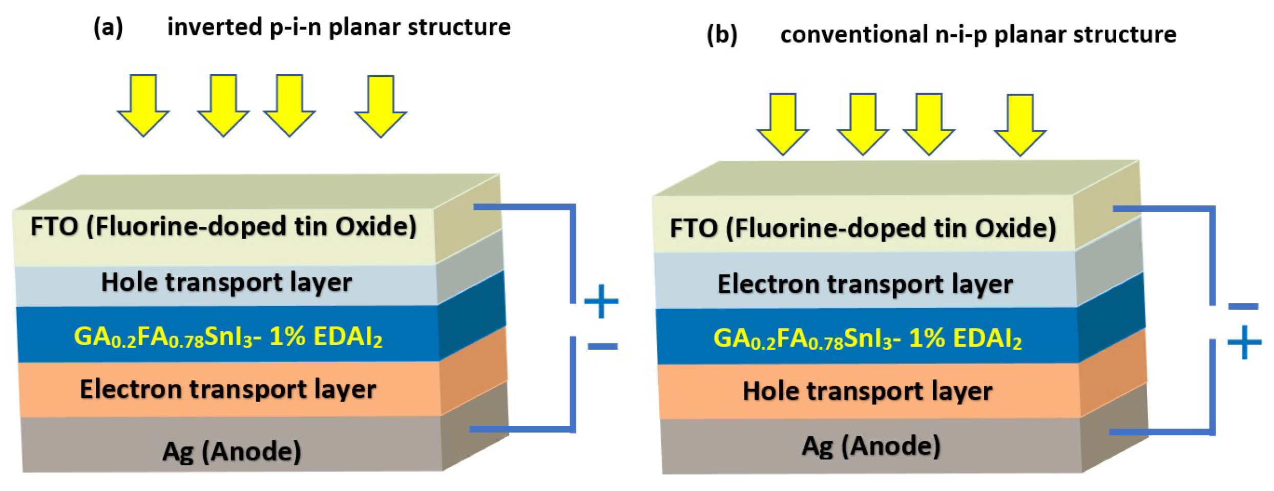
:1. Introduction
2. Materials and Methods
- Short-circuit current density J mA/cm;
- Power conversion efficiency PCE ;
- Open-circuit voltage VV;
- Fill factor FF .
3. Results and Discussion
3.1. The HTL Material Impact on the Solar Cell Performance
3.1.1. Impact of HTL Thickness
3.1.2. Impact of HTL Doping Concentration
3.2. The ETL Material Impact on the Solar Cell Performance
3.2.1. Impact of ETL Thickness
3.2.2. Impact of ETL Doping Concentration
3.3. The Absorber Impact on the Solar Cell Performance
3.3.1. Effect of the Absorber Thickness
3.3.2. Effect of the Absorber Doping Concentration
4. Conclusions
Author Contributions
Funding
Institutional Review Board Statement
Informed Consent Statement
Data Availability Statement
Acknowledgments
Conflicts of Interest
Abbreviations
| PSC | perovskite solar cell |
| PCE | power conversion efficiency |
| E1G20 | GAFASnI-1% EDAI |
| HTL | hole transport layer |
| ETL | electron transport layer |
| V | open circuit voltage |
| J | short-circuit current density |
| QE | quantum efficiency |
| FF | fill factor |
| FTO | Fluorine-doped tin oxide |
| VBO | valence band offset |
| N | acceptor doping concentration |
| CBO | conducting band offset |
| N | donor doping concentration |
References
- Kojima, A.; Teshima, K.; Shirai, Y.; Miyasaka, T. Organometal halide perovskites as visible-light sensitizers for photovoltaic cells. J. Am. Chem. Soc. 2009, 131, 6050–6051. [Google Scholar] [CrossRef] [PubMed]
- Becker, M.; Klüner, T.; Wark, M. Formation of hybrid ABX 3 perovskite compounds for solar cell application: First-principles calculations of effective ionic radii and determination of tolerance factors. Dalton Trans. 2017, 46, 3500–3509. [Google Scholar] [CrossRef] [PubMed]
- Kim, H.S.; Lee, C.R.; Im, J.H.; Lee, K.B.; Moehl, T.; Marchioro, A.; Moon, S.J.; Humphry-Baker, R.; Yum, J.H.; Moser, J.E.; et al. Lead iodide perovskite sensitized all-solid-state submicron thin film mesoscopic solar cell with efficiency exceeding 9%. Sci. Rep. 2012, 2, 591. [Google Scholar] [CrossRef] [PubMed] [Green Version]
- Galkowski, K.; Mitioglu, A.; Miyata, A.; Plochocka, P.; Portugall, O.; Eperon, G.E.; Wang, J.T.W.; Stergiopoulos, T.; Stranks, S.D.; Snaith, H.J.; et al. Determination of the exciton binding energy and effective masses for methylammonium and formamidinium lead tri-halide perovskite semiconductors. Energy Environ. Sci. 2016, 9, 962–970. [Google Scholar] [CrossRef] [Green Version]
- Zhang, W.; Anaya, M.; Lozano, G.; Calvo, M.E.; Johnston, M.B.; Míguez, H.; Snaith, H.J. Highly efficient perovskite solar cells with tunable structural color. Nano Lett. 2015, 15, 1698–1702. [Google Scholar] [CrossRef] [Green Version]
- Gottesman, R.; Haltzi, E.; Gouda, L.; Tirosh, S.; Bouhadana, Y.; Zaban, A.; Mosconi, E.; De Angelis, F. Extremely slow photoconductivity response of CH3NH3PbI3 perovskites suggesting structural changes under working conditions. J. Phys. Chem. Lett. 2014, 5, 2662–2669. [Google Scholar] [CrossRef] [Green Version]
- Gao, W.; Ran, C.; Li, J.; Dong, H.; Jiao, B.; Zhang, L.; Lan, X.; Hou, X.; Wu, Z. Robust stability of efficient lead-free formamidinium tin iodide perovskite solar cells realized by structural regulation. J. Phys. Chem. Lett. 2018, 9, 6999–7006. [Google Scholar] [CrossRef] [Green Version]
- Konstantakou, M.; Stergiopoulos, T. A critical review on tin halide perovskite solar cells. J. Mater. Chem. A 2017, 5, 11518–11549. [Google Scholar] [CrossRef]
- Sabbah, H. Numerical Simulation of 30% Efficient Lead-Free Perovskite CsSnGeI3-Based Solar Cells. Materials 2022, 15, 3229. [Google Scholar] [CrossRef]
- Sabbah, H.; Arayro, J.; Mezher, R. Numerical Simulation and Optimization of Highly Stable and Efficient Lead-Free Perovskite FA1- xCsxSnI3-Based Solar Cells Using SCAPS. Materials 2022, 15, 4761. [Google Scholar] [CrossRef]
- Slavney, A.H.; Hu, T.; Lindenberg, A.M.; Karunadasa, H.I. A bismuth-halide double perovskite with long carrier recombination lifetime for photovoltaic applications. J. Am. Chem. Soc. 2016, 138, 2138–2141. [Google Scholar] [CrossRef] [PubMed]
- Stoumpos, C.C.; Frazer, L.; Clark, D.J.; Kim, Y.S.; Rhim, S.H.; Freeman, A.J.; Ketterson, J.B.; Jang, J.I.; Kanatzidis, M.G. Hybrid germanium iodide perovskite semiconductors: Active lone pairs, structural distortions, direct and indirect energy gaps, and strong nonlinear optical properties. J. Am. Chem. Soc. 2015, 137, 6804–6819. [Google Scholar] [CrossRef] [PubMed]
- Kour, R.; Arya, S.; Verma, S.; Gupta, J.; Bandhoria, P.; Bharti, V.; Datt, R.; Gupta, V. Potential substitutes for replacement of lead in perovskite solar cells: A review. Glob. Chall. 2019, 3, 1900050. [Google Scholar] [CrossRef] [PubMed] [Green Version]
- Zhang, Q.; Hao, F.; Li, J.; Zhou, Y.; Wei, Y.; Lin, H. Perovskite solar cells: Must lead be replaced—And can it be done? Sci. Technol. Adv. Mater. 2018, 19, 425–442. [Google Scholar] [CrossRef] [Green Version]
- Babayigit, A.; Duy Thanh, D.; Ethirajan, A.; Manca, J.; Muller, M.; Boyen, H.G.; Conings, B. Assessing the toxicity of Pb-and Sn-based perovskite solar cells in model organism Danio rerio. Sci. Rep. 2016, 6, 18721. [Google Scholar] [CrossRef] [PubMed]
- Babayigit, A.; Ethirajan, A.; Muller, M.; Conings, B. Toxicity of organometal halide perovskite solar cells. Nat. Mater. 2016, 15, 247–251. [Google Scholar] [CrossRef]
- Benmessaoud, I.R.; Mahul-Mellier, A.L.; Horváth, E.; Maco, B.; Spina, M.; Lashuel, H.A.; Forró, L. Health hazards of methylammonium lead iodide based perovskites: Cytotoxicity studies. Toxicol. Res. 2016, 5, 407–419. [Google Scholar] [CrossRef] [Green Version]
- Hailegnaw, B.; Kirmayer, S.; Edri, E.; Hodes, G.; Cahen, D. Rain on methylammonium lead iodide based perovskites: Possible environmental effects of perovskite solar cells. J. Phys. Chem. Lett. 2015, 6, 1543–1547. [Google Scholar] [CrossRef]
- Zhang, L.; Ju, M.G.; Liang, W. The effect of moisture on the structures and properties of lead halide perovskites: A first-principles theoretical investigation. Phys. Chem. Chem. Phys. 2016, 18, 23174–23183. [Google Scholar] [CrossRef]
- Yao, H.; Zhou, F.; Li, Z.; Ci, Z.; Ding, L.; Jin, Z. Strategies for improving the stability of tin-based perovskite (ASnX3) solar cells. Adv. Sci. 2020, 7, 1903540. [Google Scholar] [CrossRef] [Green Version]
- Zhang, Q.; Liu, S.; He, M.; Zheng, W.; Wan, Q.; Liu, M.; Liao, X.; Zhan, W.; Yuan, C.; Liu, J.; et al. Stable Lead-free Tin Halide Perovskite with Operational Stability > 1200 h by Suppressing Tin (II) Oxidation. Angew. Chem. Int. Ed. 2022, 134, e202205463. [Google Scholar]
- Ava, T.T.; Al Mamun, A.; Marsillac, S.; Namkoong, G. A review: Thermal stability of methylammonium lead halide based perovskite solar cells. Appl. Sci. 2019, 9, 188. [Google Scholar] [CrossRef] [Green Version]
- Niu, Q.; Zhang, L.; Xu, Y.; Yuan, C.; Qi, W.; Fu, S.; Ma, Y.; Zeng, W.; Xia, R.; Min, Y. Defect Passivation Using Trichloromelamine for Highly Efficient and Stable Perovskite Solar Cells. Polymers 2022, 14, 398. [Google Scholar] [CrossRef] [PubMed]
- Ke, W.; Stoumpos, C.C.; Spanopoulos, I.; Mao, L.; Chen, M.; Wasielewski, M.R.; Kanatzidis, M.G. Efficient lead-free solar cells based on hollow {en} MASnI3 perovskites. J. Am. Chem. Soc. 2017, 139, 14800–14806. [Google Scholar] [CrossRef]
- Shao, S.; Liu, J.; Portale, G.; Fang, H.H.; Blake, G.R.; Ten Brink, G.H.; Koster, L.J.A.; Loi, M.A. Highly reproducible Sn-based hybrid perovskite solar cells with 9% efficiency. Adv. Energy Mater. 2018, 8, 1702019. [Google Scholar] [CrossRef]
- Liao, Y.; Liu, H.; Zhou, W.; Yang, D.; Shang, Y.; Shi, Z.; Li, B.; Jiang, X.; Zhang, L.; Quan, L.N.; et al. Highly oriented low-dimensional tin halide perovskites with enhanced stability and photovoltaic performance. J. Am. Chem. Soc. 2017, 139, 6693–6699. [Google Scholar] [CrossRef]
- Lee, S.J.; Shin, S.S.; Kim, Y.C.; Kim, D.; Ahn, T.K.; Noh, J.H.; Seo, J.; Seok, S.I. Fabrication of efficient formamidinium tin iodide perovskite solar cells through SnF2—Pyrazine complex. J. Am. Chem. Soc. 2016, 138, 3974–3977. [Google Scholar] [CrossRef]
- Chen, K.; Wu, P.; Yang, W.; Su, R.; Luo, D.; Yang, X.; Tu, Y.; Zhu, R.; Gong, Q. Low-dimensional perovskite interlayer for highly efficient lead-free formamidinium tin iodide perovskite solar cells. Nano Energy 2018, 49, 411–418. [Google Scholar] [CrossRef]
- Tsai, C.M.; Mohanta, N.; Wang, C.Y.; Lin, Y.P.; Yang, Y.W.; Wang, C.L.; Hung, C.H.; Diau, E.W.G. Formation of Stable Tin Perovskites Co-crystallized with Three Halides for Carbon-Based Mesoscopic Lead-Free Perovskite Solar Cells. Angew. Chem. Int. Ed. 2017, 56, 13819–13823. [Google Scholar] [CrossRef]
- Wang, F.; Ma, J.; Xie, F.; Li, L.; Chen, J.; Fan, J.; Zhao, N. Organic Cation-Dependent Degradation Mechanism of Organotin Halide Perovskites. Adv. Funct. Mater. 2016, 26, 3417–3423. [Google Scholar] [CrossRef]
- Jokar, E.; Chien, C.H.; Tsai, C.M.; Fathi, A.; Diau, E.W.G. Robust tin-based perovskite solar cells with hybrid organic cations to attain efficiency approaching 10%. Adv. Mater. 2019, 31, 1804835. [Google Scholar] [CrossRef] [PubMed]
- Liu, T.; Chen, K.; Hu, Q.; Zhu, R.; Gong, Q. Inverted perovskite solar cells: Progresses and perspectives. Adv. Energy Mater. 2016, 6, 1600457. [Google Scholar] [CrossRef]
- Jeong, J.; Kim, M.; Seo, J.; Lu, H.; Ahlawat, P.; Mishra, A.; Yang, Y.; Hope, M.A.; Eickemeyer, F.T.; Kim, M.; et al. Pseudo-halide anion engineering for α-FAPbI3 perovskite solar cells. Nature 2021, 592, 381–385. [Google Scholar] [CrossRef]
- Liu, X.; Cheng, Y.; Liu, C.; Zhang, T.; Zhang, N.; Zhang, S.; Chen, J.; Xu, Q.; Ouyang, J.; Gong, H. 20.7% highly reproducible inverted planar perovskite solar cells with enhanced fill factor and eliminated hysteresis. Energy Environ. Sci. 2019, 12, 1622–1633. [Google Scholar] [CrossRef]
- Meng, L.; You, J.; Guo, T.F.; Yang, Y. Recent advances in the inverted planar structure of perovskite solar cells. Acc. Chem. Res. 2016, 49, 155–165. [Google Scholar] [CrossRef] [PubMed]
- Jeon, N.J.; Noh, J.H.; Yang, W.S.; Kim, Y.C.; Ryu, S.; Seo, J.; Seok, S.I. Compositional engineering of perovskite materials for high-performance solar cells. Nature 2015, 517, 476–480. [Google Scholar] [CrossRef]
- Yang, W.S.; Noh, J.H.; Jeon, N.J.; Kim, Y.C.; Ryu, S.; Seo, J.; Seok, S.I. High-performance photovoltaic perovskite layers fabricated through intramolecular exchange. Science 2015, 348, 1234–1237. [Google Scholar] [CrossRef]
- Yang, W.S.; Park, B.W.; Jung, E.H.; Jeon, N.J.; Kim, Y.C.; Lee, D.U.; Shin, S.S.; Seo, J.; Kim, E.K.; Noh, J.H.; et al. Iodide management in formamidinium-lead-halide–based perovskite layers for efficient solar cells. Science 2017, 356, 1376–1379. [Google Scholar] [CrossRef] [Green Version]
- Alsalloum, A.Y.; Turedi, B.; Almasabi, K.; Zheng, X.; Naphade, R.; Stranks, S.D.; Mohammed, O.F.; Bakr, O.M. 22.8%-Efficient single-crystal mixed-cation inverted perovskite solar cells with a near-optimal bandgap. Energy Environ. Sci. 2021, 14, 2263–2268. [Google Scholar] [CrossRef]
- Sabbah, H.; Arayro, J.; Mezher, R. Simulation and Investigation of 26% Efficient and Robust Inverted Planar Perovskite Solar Cells Based on GA0.2FA0.78SnI3-1% EDAI2 Films. Nanomaterials 2022, 12, 3885. [Google Scholar] [CrossRef]
- Burgelman, M.; Nollet, P.; Degrave, S. Modelling polycrystalline semiconductor solar cells. Thin Solid Film. 2000, 361, 527–532. [Google Scholar] [CrossRef]
- Liu, X.; Yan, K.; Tan, D.; Liang, X.; Zhang, H.; Huang, W. Solvent engineering improves efficiency of lead-free tin-based hybrid perovskite solar cells beyond 9%. ACS Energy Lett. 2018, 3, 2701–2707. [Google Scholar] [CrossRef]
- Gan, Y.; Bi, X.; Liu, Y.; Qin, B.; Li, Q.; Jiang, Q.; Mo, P. Numerical investigation energy conversion performance of tin-based perovskite solar cells using cell capacitance simulator. Energies 2020, 13, 5907. [Google Scholar] [CrossRef]
- Koh, T.M.; Krishnamoorthy, T.; Yantara, N.; Shi, C.; Leong, W.L.; Boix, P.P.; Grimsdale, A.C.; Mhaisalkar, S.G.; Mathews, N. Formamidinium tin-based perovskite with low E g for photovoltaic applications. J. Mater. Chem. A 2015, 3, 14996–15000. [Google Scholar] [CrossRef]
- Kim, C.; Huan, T.D.; Krishnan, S.; Ramprasad, R. A hybrid organic-inorganic perovskite dataset. Sci. Data 2017, 4, 170057. [Google Scholar] [CrossRef] [Green Version]
- Herz, L.M. Charge-carrier mobilities in metal halide perovskites: Fundamental mechanisms and limits. ACS Energy Lett. 2017, 2, 1539–1548. [Google Scholar] [CrossRef] [Green Version]
- Abdelaziz, S.; Zekry, A.; Shaker, A.; Abouelatta, M. Investigating the performance of formamidinium tin-based perovskite solar cell by SCAPS device simulation. Opt. Mater. 2020, 101, 109738. [Google Scholar] [CrossRef]
- Shasti, M.; Mortezaali, A. Numerical study of Cu2O, SrCu2O2, and CuAlO2 as hole-transport materials for application in perovskite solar cells. Phys. Status Solidi 2019, 216, 1900337. [Google Scholar] [CrossRef]
- Patel, P.K. Device simulation of highly efficient eco-friendly CH3NH3SnI3 perovskite solar cell. Sci. Rep. 2021, 11, 3082. [Google Scholar] [CrossRef]
- Singh, A.K.; Srivastava, S.; Mahapatra, A.; Baral, J.K.; Pradhan, B. Performance optimization of lead free-MASnI3 based solar cell with 27% efficiency by numerical simulation. Opt. Mater. 2021, 117, 111193. [Google Scholar] [CrossRef]
- Madhavan, V.E.; Zimmermann, I.; Baloch, A.A.; Manekkathodi, A.; Belaidi, A.; Tabet, N.; Nazeeruddin, M.K. CuSCN as hole transport material with 3D/2D perovskite solar cells. ACS Appl. Energy Mater. 2019, 3, 114–121. [Google Scholar] [CrossRef] [Green Version]
- Liu, J.; Zhang, Y.; Liu, C.; Peng, M.; Yu, A.; Kou, J.; Liu, W.; Zhai, J.; Liu, J. Piezo-phototronic effect enhanced UV photodetector based on CuI/ZnO double-shell grown on flexible copper microwire. Nanoscale Res. Lett. 2016, 11, 281. [Google Scholar] [CrossRef] [PubMed] [Green Version]
- Du, H.J.; Wang, W.C.; Zhu, J.Z. Device simulation of lead-free CH3NH3SnI3 perovskite solar cells with high efficiency. Chin. Phys. B 2016, 25, 108802. [Google Scholar] [CrossRef]
- Stamate, M.D. On the dielectric properties of dc magnetron TiO2 thin films. Appl. Surf. Sci. 2003, 218, 318–323. [Google Scholar] [CrossRef]
- Sobayel, K.; Akhtaruzzaman, M.; Rahman, K.; Ferdaous, M.; Al-Mutairi, Z.A.; Alharbi, H.F.; Alharthi, N.H.; Karim, M.R.; Hasmady, S.; Amin, N. A comprehensive defect study of tungsten disulfide (WS2) as electron transport layer in perovskite solar cells by numerical simulation. Results Phys. 2019, 12, 1097–1103. [Google Scholar] [CrossRef]
- Zhang, Y.; Blom, P.W. Electron and hole transport in poly (fluorene-benzothiadiazole). Appl. Phys. Lett. 2011, 98, 143504. [Google Scholar] [CrossRef] [Green Version]
- Baena, J.P.C.; Steier, L.; Tress, W.; Saliba, M.; Neutzner, S.; Matsui, T.; Giordano, F.; Jacobsson, T.J.; Kandada, A.R.S.; Zakeeruddin, S.M.; et al. Highly efficient planar perovskite solar cells through band alignment engineering. Energy Environ. Sci. 2015, 8, 2928–2934. [Google Scholar] [CrossRef] [Green Version]
- Farahani, S.V.; Veal, T.; Mudd, J.; Scanlon, D.; Watson, G.; Bierwagen, O.; White, M.; Speck, J.; McConville, C. Valence-band density of states and surface electron accumulation in epitaxial SnO2 films. Phys. Rev. B 2014, 90, 155413. [Google Scholar] [CrossRef] [Green Version]
- Li, C.Z.; Chang, C.Y.; Zang, Y.; Ju, H.X.; Chueh, C.C.; Liang, P.W.; Cho, N.; Ginger, D.S.; Jen, A.K.Y. Suppressed charge recombination in inverted organic photovoltaics via enhanced charge extraction by using a conductive fullerene electron transport layer. Adv. Mater. 2014, 26, 6262–6267. [Google Scholar] [CrossRef]
- Zhou, H.; Chen, Q.; Li, G.; Luo, S.; Song, T.B.; Duan, H.S.; Hong, Z.; You, J.; Liu, Y.; Yang, Y. Interface engineering of highly efficient perovskite solar cells. Science 2014, 345, 542–546. [Google Scholar] [CrossRef] [PubMed]
- Arumugam, G.M.; Karunakaran, S.K.; Liu, C.; Zhang, C.; Guo, F.; Wu, S.; Mai, Y. Inorganic hole transport layers in inverted perovskite solar cells: A review. Nano Sel. 2021, 2, 1081–1116. [Google Scholar] [CrossRef]
- Roy, P.; Dongre, Y.; Tiwari, S.; Chaturvedi, D.; Khare, A. Impact of hole transport layer on the performance of all-inorganic tin (Sn) based perovskite solar cells. In Proceedings of the IOP Conference Series: Materials Science and Engineering, Sanya, China, 12–14 November 2021; IOP Publishing: Bristol, UK, 2021; Volume 1120, p. 012016. [Google Scholar]
- Ke, W.; Priyanka, P.; Vegiraju, S.; Stoumpos, C.C.; Spanopoulos, I.; Soe, C.M.M.; Marks, T.J.; Chen, M.C.; Kanatzidis, M.G. Dopant-free tetrakis-triphenylamine hole transporting material for efficient tin-based perovskite solar cells. J. Am. Chem. Soc. 2018, 140, 388–393. [Google Scholar] [CrossRef] [PubMed]
- Ng, C.H.; Nishimura, K.; Ito, N.; Hamada, K.; Hirotani, D.; Wang, Z.; Yang, F.; Shen, Q.; Yoshino, K.; Minemoto, T.; et al. Role of GeI2 and SnF2 additives for SnGe perovskite solar cells. Nano Energy 2019, 58, 130–137. [Google Scholar] [CrossRef]
- Tan, H.; Jain, A.; Voznyy, O.; Lan, X.; García de Arquer, F.P.; Fan, J.Z.; Quintero-Bermudez, R.; Yuan, M.; Zhang, B.; Zhao, Y.; et al. Efficient and stable solution-processed planar perovskite solar cells via contact passivation. Science 2017, 355, 722–726. [Google Scholar] [CrossRef]
- Kim, G.W.; Shinde, D.V.; Park, T. Thickness of the hole transport layer in perovskite solar cells: Performance versus reproducibility. RSC Adv. 2015, 5, 99356–99360. [Google Scholar] [CrossRef]
- Srivastava, R.P.; Jung, H.S.; Khang, D.Y. Transfer-Printed Cuprous Iodide (CuI) Hole Transporting Layer for Low Temperature Processed Perovskite Solar Cells. Nanomaterials 2022, 12, 1467. [Google Scholar] [CrossRef] [PubMed]
- Wang, H.; Yu, Z.; Jiang, X.; Li, J.; Cai, B.; Yang, X.; Sun, L. Efficient and stable inverted planar perovskite solar cells employing CuI as hole-transporting layer prepared by solid—Gas transformation. Energy Technol. 2017, 5, 1836–1843. [Google Scholar] [CrossRef] [Green Version]
- Bag, A.; Radhakrishnan, R.; Nekovei, R.; Jeyakumar, R. Effect of absorber layer, hole transport layer thicknesses, and its doping density on the performance of perovskite solar cells by device simulation. Sol. Energy 2020, 196, 177–182. [Google Scholar] [CrossRef]
- Nguyen, W.H.; Bailie, C.D.; Unger, E.L.; McGehee, M.D. Enhancing the hole-conductivity of spiro-OMeTAD without oxygen or lithium salts by using spiro (TFSI)2 in perovskite and dye-sensitized solar cells. J. Am. Chem. Soc. 2014, 136, 10996–11001. [Google Scholar] [CrossRef]
- Warby, J.; Zu, F.; Zeiske, S.; Gutierrez-Partida, E.; Frohloff, L.; Kahmann, S.; Frohna, K.; Mosconi, E.; Radicchi, E.; Lang, F.; et al. Understanding performance limiting interfacial recombination in pin perovskite solar cells. Adv. Energy Mater. 2022, 12, 2103567. [Google Scholar] [CrossRef]
- Rai, N.; Rai, S.; Singh, P.K.; Lohia, P.; Dwivedi, D. Analysis of various ETL materials for an efficient perovskite solar cell by numerical simulation. J. Mater. Sci. Mater. Electron. 2020, 31, 16269–16280. [Google Scholar] [CrossRef]
- Xu, L.; Molaei Imenabadi, R.; Vandenberghe, W.G.; Hsu, J.W. Minimizing performance degradation induced by interfacial recombination in perovskite solar cells through tailoring of the transport layer electronic properties. APL Mater. 2018, 6, 036104. [Google Scholar] [CrossRef] [Green Version]
- Liu, W.; Liu, N.; Ji, S.; Hua, H.; Ma, Y.; Hu, R.; Zhang, J.; Chu, L.; Li, X.; Huang, W. Perfection of perovskite grain boundary passivation by rhodium incorporation for efficient and stable solar cells. Nano-Micro Lett. 2020, 12, 119. [Google Scholar] [CrossRef]
- Liu, W.; Feng, Y.; Li, L.; Ma, Y.; Hu, R.; Wu, X.; Chu, L.; Li, X.; Huang, W. Stable and Efficient Pb—Ni Binary Metal Perovskite Solar Cells. ACS Sustain. Chem. Eng. 2021, 9, 17112–17119. [Google Scholar] [CrossRef]


| Parameters | E1G20 [31,44,45,46,47] | PEDOT:PSS (HTL) [31,42,43] | C60 (ETL) [31,42,43] |
|---|---|---|---|
| Thickness/μm | 0.35 | 0.1 | 0.05 |
| Bandgap E/eV | 1.5 | 2.2 | 1.7 |
| Electron affinity /eV | 3.7 | 2.9 | 3.9 |
| Dielectric permittivity | 8.2 | 2.3 | 4.2 |
| CB effective density of states/cm | |||
| VB effective density of states/cm | |||
| Electron mobility/cm/V·s | 22 | 0.08 | |
| Hole mobility/cm/V·s Donor concentration N/cm | 0 | 0 | |
| Acceptor concentration N/cm | 0 |
| Parameters | CuO [48,49] | CuSCN [50,51] | CuI [50,52] |
|---|---|---|---|
| Thickness/μm | 0.1 | 0.1 | 0.1 |
| Bandgap E/eV | 2.170 | 3.4 | 3.4 |
| Electron affinity /eV | 3.2 | 1.9 | 2.1 |
| Dielectric permittivity | 7.11 | 10 | 10 |
| CB effective density of states/cm | |||
| VB effective density of states/cm | |||
| Electron mobility/cm/V·sHole mobility/cm/V·s Donor concentration N/cm | 0 | 0 | 0 |
| Acceptor concentration N/cm |
| Parameters | TiO [53,54] | ZnOS [50] | WS [55,56] | SnO [57,58] |
|---|---|---|---|---|
| Thickness/μm | 0.05 | 0.05 | 0.05 | 0.05 |
| Bandgap E/eV | 3.26 | 2.83 | 1.80 | 3.60 |
| Electron affinity /eV | 4 | 3.60 | 3.95 | 3.93 |
| Dielectric permittivity | 32 | 9 | 13.6 | 8 |
| CB effective density of states/cm | ||||
| VB effective density of states/cm | ||||
| Electron mobility/cm/V·s Hole mobility/cm/V·s Donor concentration N/cm | ||||
| Acceptor concentration N/cm | 0 | 0 | 0 | 0 |
| Parameters | HTL | ETL | E1G20 | HTL/E1G20 | E1G20/ETL |
|---|---|---|---|---|---|
| Defect Type | Neutral | Neutral | Neutral | Neutral | Neutral |
| Capture cross section for electrons /cm | |||||
| Capture cross section for holes /cm | |||||
| Energetic distribution | Single | Single | Gaussian | Single | Single |
| Energy level with respect to E (above E)/eV | 0.650 | 0.65 | 0.6 | 0.6 | 0.6 |
| Characteristic energy/eV | 0.1 | 0.1 | 0.1 | 0.1 | 0.1 |
| Total density N/cm |
| HTL | VBO/eV |
|---|---|
| PEDOT:PSS (Reference cell) | −0.1 |
| CuO | 0.2 |
| CuI | 0.3 |
| CuSCN | 0.1 |
Disclaimer/Publisher’s Note: The statements, opinions and data contained in all publications are solely those of the individual author(s) and contributor(s) and not of MDPI and/or the editor(s). MDPI and/or the editor(s) disclaim responsibility for any injury to people or property resulting from any ideas, methods, instructions or products referred to in the content. |
© 2023 by the authors. Licensee MDPI, Basel, Switzerland. This article is an open access article distributed under the terms and conditions of the Creative Commons Attribution (CC BY) license (https://creativecommons.org/licenses/by/4.0/).
Share and Cite
Arayro, J.; Mezher, R.; Sabbah, H. Comparative Simulation Study of the Performance of Conventional and Inverted Hybrid Tin-Based Perovskite Solar Cells. Coatings 2023, 13, 1258. https://doi.org/10.3390/coatings13071258
Arayro J, Mezher R, Sabbah H. Comparative Simulation Study of the Performance of Conventional and Inverted Hybrid Tin-Based Perovskite Solar Cells. Coatings. 2023; 13(7):1258. https://doi.org/10.3390/coatings13071258
Chicago/Turabian StyleArayro, Jack, Rabih Mezher, and Hussein Sabbah. 2023. "Comparative Simulation Study of the Performance of Conventional and Inverted Hybrid Tin-Based Perovskite Solar Cells" Coatings 13, no. 7: 1258. https://doi.org/10.3390/coatings13071258
APA StyleArayro, J., Mezher, R., & Sabbah, H. (2023). Comparative Simulation Study of the Performance of Conventional and Inverted Hybrid Tin-Based Perovskite Solar Cells. Coatings, 13(7), 1258. https://doi.org/10.3390/coatings13071258