Article

Characterization of CdS/CdTe Ultrathin-Film Solar Cells with Different CdS Thin-Film Thicknesses Obtained by RF Sputtering

by
J. A. Melchor-Robles
1,
K. E. Nieto-Zepeda
2,*,
N. E. Vázquez-Barragán
2,
M. Arreguín-Campos
3,
K. Rodríguez-Rosales
2,
J. Cruz-Gómez
4,
A. Guillén-Cervantes
5,
J. Santos-Cruz
2,
M. de la L. Olvera
6,
G. Contreras-Puente
4 and
F. de Moure-Flores
2,*
1
Nanociencias y Nanotecnología, CINVESTAV-IPN, Ciudad de México 07360, Mexico
2
Facultad de Química, Energía-Materiales, Universidad Autónoma de Querétaro, Santiago de Querétaro 76010, Mexico
3
Advanced Functional Polymers Group, Department of Chemistry, Institute for Materials Research (IMO), Hasselt University, 3500 Hasselt, Belgium
4
Escuela Superior de Física y Matemáticas del Instituto Politécnico Nacional, Ciudad de México 07738, Mexico
5
Departamento de Física, CINVESTAV-IPN, Apdo. Postal 14-740, Ciudad de México 07360, Mexico
6
Departamento de Ingeniería Eléctrica, Sección de Estado Sólido, CINVESTAV-IPN, Apdo. Postal 14-740, Ciudad de México 07360, Mexico
*
Authors to whom correspondence should be addressed.
Coatings 2024, 14(4), 452; https://doi.org/10.3390/coatings14040452
Submission received: 11 October 2023 / Revised: 18 February 2024 / Accepted: 29 March 2024 / Published: 9 April 2024
(This article belongs to the Special Issue Functional Layers in Thin Film Photovoltaics and Solar Energy)

Abstract

:
The development of semitransparent CdS/CdTe ultrathin solar cells has been delayed as a result of the activation annealing to which the device must be subjected, which may involve problems such as the sublimation of ultrathin films and the diffusion of Cd and S at the interface. In this work, CdS/CdTe ultrathin devices on soda-lime glass/SnO2:F/ZnO substrates were obtained by RF magnetron sputtering. CdS/CdTe ultrathin heterostructures were obtained with the following thicknesses for the CdS thin film: 70, 110, and 135 nm. The CdTe thickness film was kept constant at 620 nm. Subsequently, activation annealing with CdCl2 was carried out at 400 °C. Surface characterization was performed by scanning electron microscopy, which indicated that the CdCl2 annealing tripled the CdTe thin films’ grain size. Raman characterization showed that CdS thin films deposited by RF sputtering present the first, the second, and the third longitudinal optical modes, indicating the good crystallinity of the CdS thin films. The study showed that the photovoltaic properties of the CdS/CdTe ultrathin devices improved as the CdS thicknesses decreased.

1. Introduction

Thin-film solar cell technology has proven to be one of the most promising photovoltaic technologies for converting solar energy into electricity, owing to its high efficiency and the advantage of easy, large-scale production. Specifically, CdS/CdTe-based thin-film solar cells are among the most important heterostructures due to their high power conversion with theoretical efficiencies projected up to 28%–30% [1], and above 22% for experimental cells [2], resulting from their ability to absorb the majority of the incoming photons, high stability and low-cost fabrication [3]. CdS thin films are commonly employed as a window layer in CdTe cells due to their wide direct bandgap (~2.40 eV), which results in good transparency in the visible region, and n-type conductivity [4,5], allowing for a high fraction of light to reach the CdTe p-type semiconductor. A typical CdS/CdTe solar cell uses a thick CdTe layer of 5–10 µm with a nearly optimal bandgap (~1.45 eV) and a high absorption coefficient of 105 cm−1 [5,6]. However, it is desirable to decrease CdTe thickness to less than 1 µm, reducing the material’s consumption and production cost [7,8]. This decrement in the CdTe layer also has other benefits, such as reducing the loss of minority charge carriers, and increasing the amount of light transmission in the visible range, which could expand its application [9]. Furthermore, employing CdS nanowires instead of CdS thin films has proven to be a promising alternative. CdS nanowires/CdTe solar cells have demonstrated improvements in conversion efficiencies, attributed to enhancements in quantum efficiency. Nonetheless, the long-term stability of CdS nanowires remains an unexplored field [10]. Recent research has focused on partially transparent CdS/CdTe ultrathin solar cells due to their multiple applications, such as in bifacial power generation, in tandem configurations to promote the utilization of sunlight, and their integration in windows on buildings and vehicles [11]. Building-integrated photovoltaics (BIPV), such as solar roofs and building windows, can help to generate power while helping to control light and provide thermal insulation [12,13,14,15]. For these mentioned applications, it should be noted that ultrathin CdS/CdTe solar cells must have the highest possible efficiencies (assuming that a significant part of the radiation is not absorbed into the cell) and good optical properties in the visible region, depending on their application [14]. In order to improve the efficiency of CdS/CdTe solar cells, a reduction in the thickness of the CdS thin film can diminish losses in quantum efficiency [16]. However, decreasing the thickness of the CdS layer below 100 nm can cause the presence of pinholes and discontinuities [16], hence special care must be taken when choosing a deposition technique to reduce the CdS film thickness. CdS and CdTe thin films, as well as solar cells based on these semiconductors, have been prepared by different deposition techniques [17], both physical and chemical [5,18], which play an essential role in the properties of a particular application. RF magnetron sputtering technique has unique advantages such as simple operation, high reproducibility, the possibility of applying low- or high-deposition temperatures, and control over film thickness. Additionally, it allows for the sequential deposition of semiconductor materials in the form of thin films without breaking vacuum conditions and for reasonable control of small growth rates (beneficial for the deposition of ultrathin layers). It does not generate waste, which makes it possible to obtain ultrathin films with good crystalline quality [14,15,19]. On the other hand, the insertion of a ZnO buffer layer in the CdTe-based solar heterostructure as part of the window layer has been shown to play an indispensable role in the conversion efficiency. This is due to the high transmittance derived from its high bandgap (~3.3 eV), excellent electrical and optical properties, abundance, good conduction band alignment with the SnO2:F and CdS materials, as well as its high electrochemical and thermal stability [20,21].
In this work, CdS and CdTe thin films were obtained by RF sputtering with a thickness optimized for the requirements of ultrathin solar cells. CdS thickness strongly limits CdTe solar cell performance. Therefore, the following three different thicknesses were evaluated for the CdS layer: 70, 110, and 135 nm. The thickness of the CdTe film was kept constant at 620 nm. Solar cell devices were fabricated onto soda-lime glass/SnO2:F/ZnO substrates by adding metallic back contacts of Cu/Au with a diameter of 3 mm.

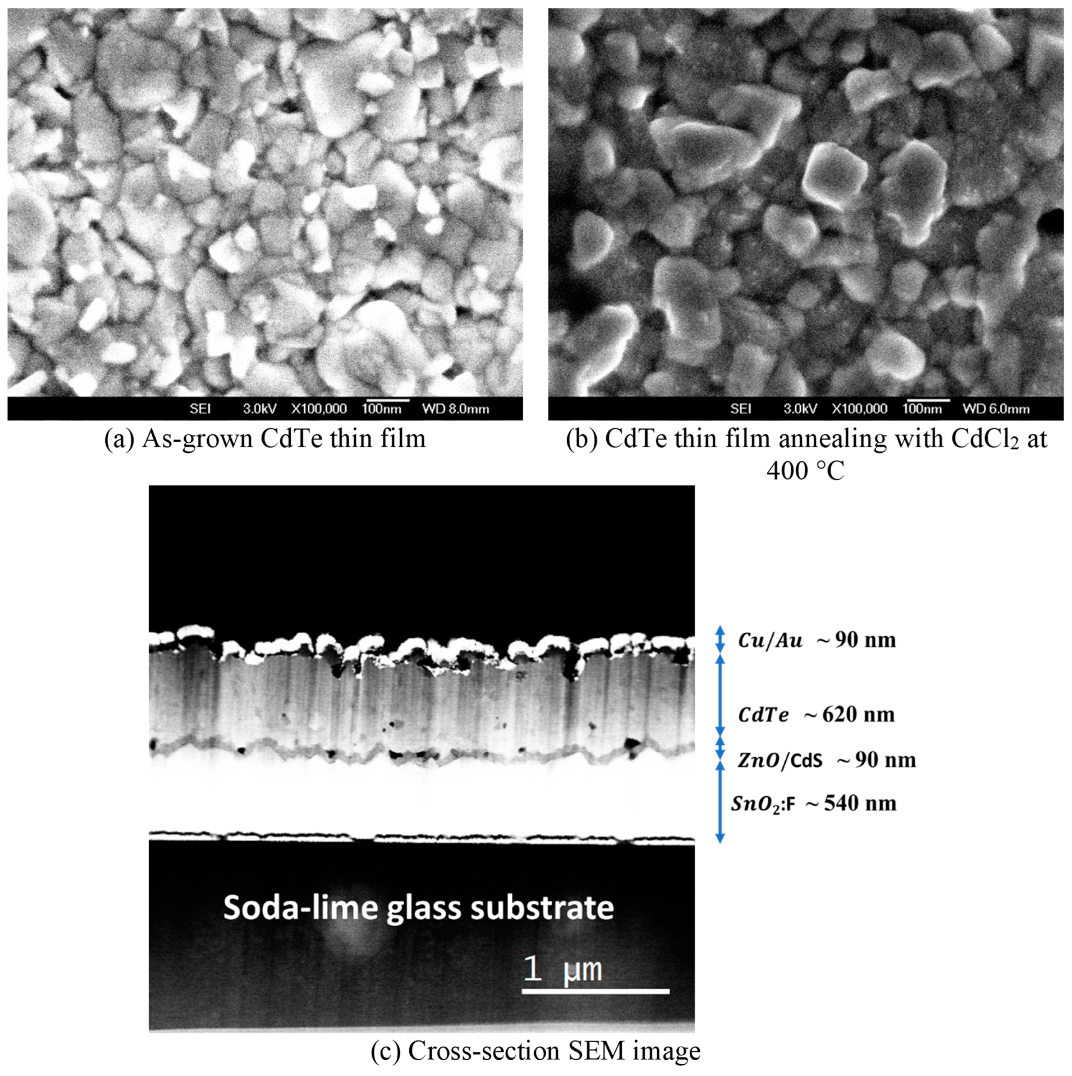
2. Materials and Methods

Ultrathin films were prepared by RF magnetron sputtering on commercial soda-lime glass/SnO2:F with a sheet resistance of 10 Ω/□ and a thickness of 0.5 µm. ZnO, CdS, and CdTe thin films were deposited employing ZnO, CdS, and CdTe commercial targets from Kurt J. Lesker, with a diameter of 3 inches. ZnO, CdS, and CdTe thin films were deposited with an Ar flow rate of 10 sccm and a substrate temperature of 300 °C. First, a ZnO ultrathin film was deposited with a thickness of ~20 nm; thereby, the glass/SnO2:F/ZnO heterostructure was obtained. Subsequently, CdS thin films were deposited at 25 W for 90, 105, and 120 min on glass/SnO2:F/ZnO substrates to obtain the glass/SnO2:F/ZnO/CdS heterostructures. Then, CdTe ultrathin films were deposited at 50 W for 4.5 h to obtain glass/SnO2:F/ZnO/CdS/CdTe heterostructures. The activation annealing was carried out with CdCl2 vapors at 400 °C in a vacuum chamber. After the annealing with CdCl2, the glass/SnO2:F/ZnO/CdS/CdTe heterostructures were exposed to high-purity methanol vapors to eliminate the residues of CdCl2. Then, metallic back contacts of Cu/Au with a diameter of 3 mm were placed onto the CdTe ultrathin film and annealed at 150 °C in vacuum conditions. Thus, glass/SnO2:F/ZnO/CdS/CdTe/Cu/Au devices with different CdS thin-film thicknesses were obtained.
The film thicknesses were measured by a profilometer KLA Tencor P15. The composition of CdS was measured by energy dispersive spectrometry (EDS) with a Bruker XFlash 5010 detector installed in a JSM-6300 scanning electron microscope from JEOL, using an accelerating voltage of 20 kV. Field emission scanning electron microscopy (FE-SEM) images were recorded using a JEOL JSM-7401F, operated at 2 kV, with a working distance of 8 mm. CdS ultrathin films were structurally characterized by a Raman spectrophotometer DRX2 from ThermoScientific using a 532 nm laser source. The transmittance spectra were measured at room temperature with a UV–Vis spectrophotometer (Genesys 10S, Thermo Scientific, Waltham, MA, USA). Photoluminescence (PL) spectra were acquired at room temperature with an excitation wavelength of 325 nm utilizing a He-Cd laser in a working range of 500–950 nm. The PL signal passed through a Spex 1404 spectrophotometer and was received by a photomultiplier detector.
X-ray patterns of CdS/CdTe heterostructures were obtained with an X-Pert Pro de Panalytical diffractometer, using the Cu-Kα line of 1.5406 Å. The current density versus voltage (J–V) measurements were obtained with an Oriel solar simulator (Newport model 91160) using an AM1.5 filter and a radiation intensity of 100 mW/cm2.

3. Results and Discussion

3.1. CdS Thin Films Deposited at Different Thicknesses

The thickness of the CdS films deposited by RF sputtering increased as the growth time increased. The thickness of CdS film deposited at 90 min was 70 nm, and it incremented up to 110 nm with a deposition time of 105 min, whereas for the CdS thin film deposited at 120 min, the thickness reached 135 nm. The samples were labeled according to the thicknesses of the CdS films. The Cd and S atomic contents of CdS thin films deposited at different thicknesses by RF sputtering are displayed in Table 1. Note that CdS thin films have a Cd excess, suggesting sulfur deficiencies. Moreover, as the thickness increases, the Cd atomic content decreased from 57.43 to 53.19%, which corroborated that the CdS thin films deposited by RF sputtering had S vacancies. Furthermore, the Cd:S ratio decreased from 1.35 to 1.14, as the CdS thickness increased (see Table 1). This indicates that increments in the CdS thickness promotes stoichiometric growth of CdS thin films, as observed in samples CdS-110 and CdS-135 [22]. It is worth noting that the CdS thin film with a thickness of 70 nm exhibits high sulfur deficiencies. This implies that devices with a 70 nm-thick CdS film may experience improved efficiency. The SEM image of a CdS thin film with a thickness of 70 nm is shown in Figure 1. The CdS-70 sample surface presents semi-spherical grains with an average diameter of 33 nm. CdS thin films deposited by RF sputtering usually have spherical and small grains, ranging from 10 nm to 60 nm [23]. No cracks or major imperfections, such as pinholes, are visible on the surface of the CdS-70 sample, demonstrating the suitability of this deposition technique for the growth of ultrathin films. SEM micrographs of the CdS-110 and CdS-135 are not included because they exhibited similar morphological characteristics to the CdS film with a thickness of 70 nm (see Figure 1).
Raman spectra of CdS ultrathin films deposited by RF magnetron sputtering at different thicknesses are shown in Figure 2. Spectra of the CdS thin films had the following three signals: the first longitudinal optical mode (LO) associated with hexagonal CdS was observed at ~300 cm−1; the second harmonic (2LO) was observed at ~600 cm−1; and the third (3LO) was observed at ~900 cm−1. The presence of the second and third vibrational modes indicates good crystallinity in the CdS thin films [15]. It is important to mention that, in ambient conditions, the CdS can present both cubic and hexagonal phases.
The optical transmittance spectra of CdS thin films obtained by RF magnetron sputtering with different thicknesses are shown in Figure 3a. The transmittance of CdS ultrathin films decreases slightly as the thickness increases, as expected; the greater the thickness, the lower the transmittance percentage. This is because thicker CdS films contain more atoms in their structure, leading to a greater availability of states for photon absorption. Thus, the CdS films deposited with a thickness of 70 and 110 nm exhibit high transmittance percentages between 50%–85% in the visible region of the electromagnetic spectrum, while the percentage transmittance of the CdS-135 sample decreases by 7%. The high transmittance of the CdS-70 sample is associated with its lower thickness, which results in fewer electronic states made available for photon absorption [24,25,26]. The similarity between the transmittance spectra of the CdS-70 and CdS-110 samples could indicate similar physical and surface qualities. On the contrary, the CdS thin film with 135 nm could have a greater availability of states that can interact with the photons, causing less light to pass through. Moreover, it can be characterized by an irregular and rougher surface, allowing more light scattering. Therefore, there is a notorious decrement in its transmittance. These transmittance results are important because ultrathin films are characterized by a high transmission, which increases the photon density at the CdS/CdTe interface of a solar cell. The bandgap estimation was made using Tauc’s parabolic bands model by fitting of the linear portion of the versus the (αhν)2 curve [15]. The bandgap of CdS thin films increased from 2.24 eV to 2.42 eV as the film thickness increased from 70 to 135 nm, respectively. The notable increment in the bandgap of the CdS film with a thickness of 135 nm can be attributed to an enhancement in the density of localized states in the conduction band, which is related to the availability of states increasing with the CdS film’s thickness [15], as mentioned previously. Additionally, this increment in the bandgap as a function of the CdS thickness is also correlated to structural parameters such as crystallite size or high lattice microstrain [27]. The bandgap values are close to 2.42 eV, the most-reported bandgap value for CdS at room temperature [5].
Photoluminescence (PL) spectra of CdS ultrathin films deposited by RF magnetron sputtering with different thicknesses are shown in Figure 3b. The PL spectra have two bands centered at 1.77 and 2.27 eV. The signal at 1.77 eV is known as the red band, while the signal at 2.27 eV is known as the green band [5]. The red signal corresponds to sulfur vacancies, whereas the green band originates in radiative transitions due to sulfur vacancies near the bottom of the conduction band to the top of the valence band, radiative recombination between donor–acceptor pairs as long as the second ionization states of sulfur vacancies or interstitial sulfur [5,28]. The intensity of the red band decreases as the thickness increases, which suggests that increasing the CdS thickness reduces the sulfur vacancies. This agrees well with the atomic composition discussion (see Table 1). It is important to note that CdS thin films with high intensity in the red band have been used in high-efficiency CdTe solar cells. The intensity of the red band can be related to the number of sulfur vacancies, and the sulfur vacancies improve the electrical properties of CdS thin films due to the rise in carriers [28,29,30,31].

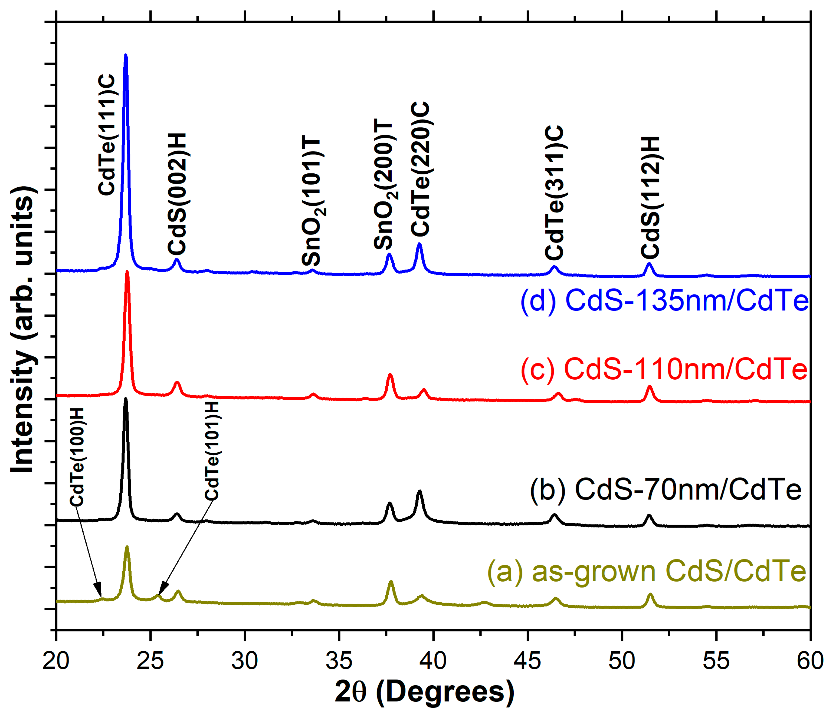
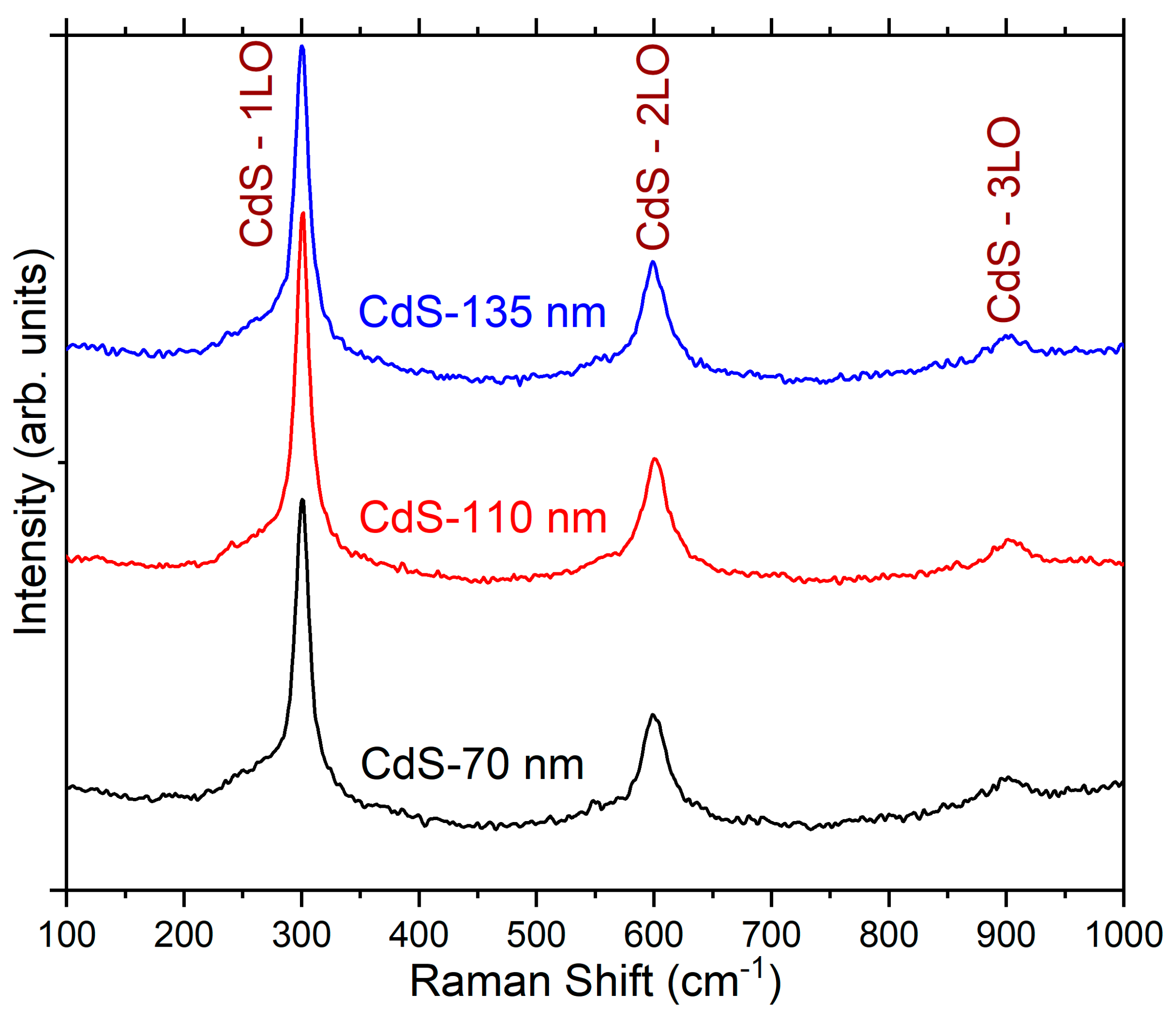
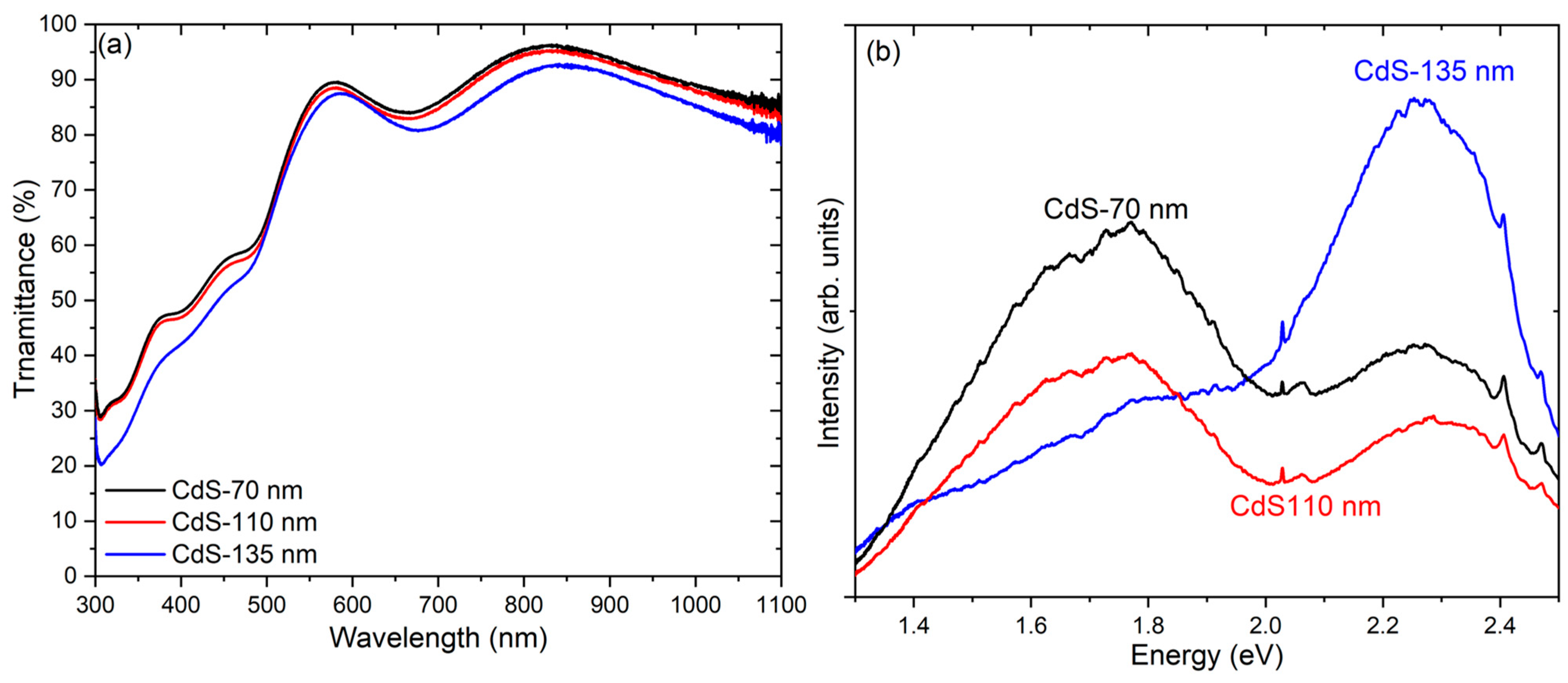
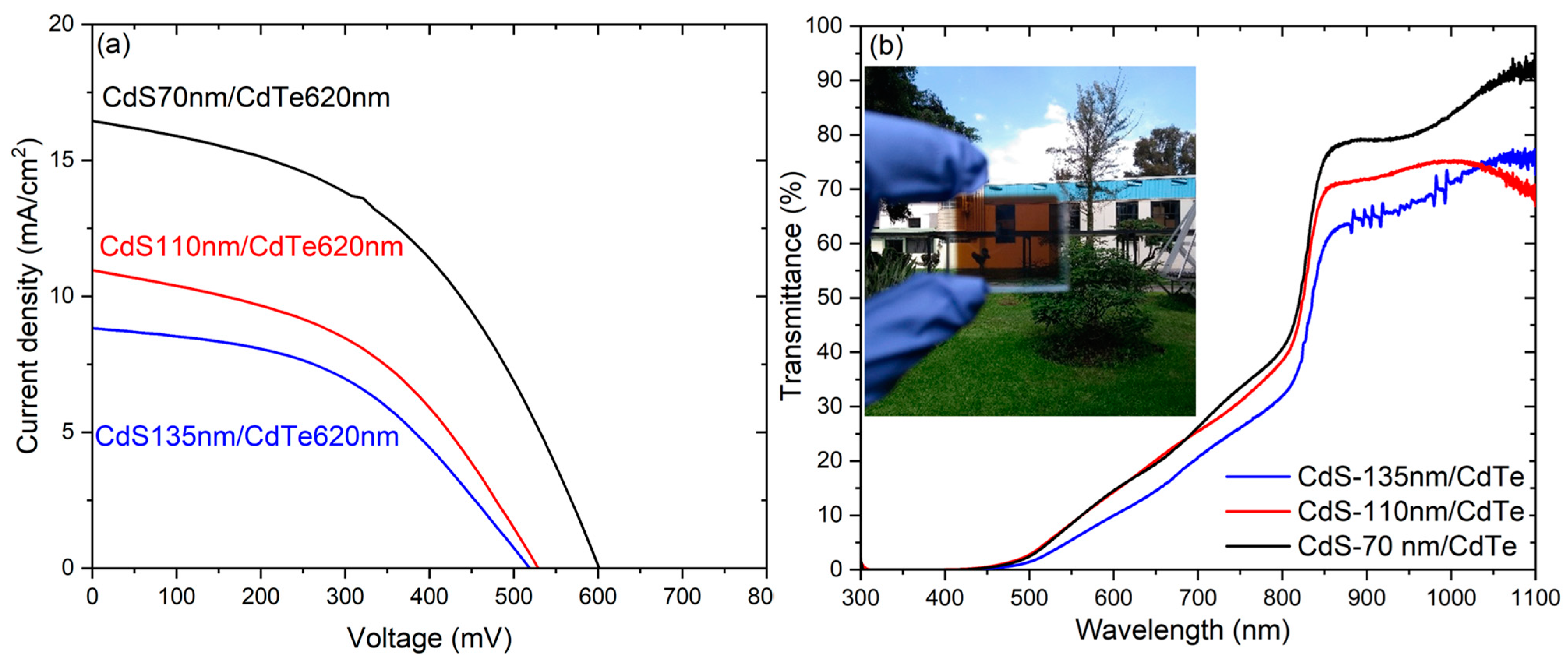
3.2. Characterization of SnO2:F/ZnO/CdS/CdTe Heterostructures with Different CdS Thicknesses

XRD patterns of SnO2:F/ZnO/CdS/CdTe heterostructures grown by RF sputtering with different CdS thicknesses are shown in Figure 4. It is important to note that CdS/CdTe heterostructures have a CdTe ultrathin film with a thickness of 620 nm. The XRD pattern of the SnO2:F/ZnO/CdS/CdTe heterostructure without CdCl2 annealing is shown in Figure 4a. It is noteworthy that the diffractogram has two diffraction planes related to the CdTe hexagonal phase (PDF#19-0193). However, when the SnO2:F/ZnO/CdS/CdTe devices are subjected to CdCl2 activation annealing, the diffraction planes associated with the hexagonal structure of CdTe are completely suppressed, giving rise to the prominent peak (111) attributed to the CdTe cubic structure, which becomes more intense (see Figure 4b–d). These XRD results indicate that CdTe ultrathin films, annealing with CdCl2 at 400 °C, are characterized by the CdTe cubic phase (PDF#15-0770). The cubic crystal structure of CdTe has been associated with favorable efficiencies in ultrathin solar devices [31,32]. Additionally, the diffractograms in Figure 4a–d show low-intensity signals corresponding to the CdS hexagonal phase (PDF#65-3414) as well as some others in the SnO2:F tetragonal phase (PDF#41-1445) correlated to the SnO2:F/ZnO/CdS substrate. Moreover, it is evident that the intensity of the CdS (002) plane increases slightly as the CdS film thickness increases. This fact can be attributed to the sensitivity of the XRD technique to increments of the CdS material present, derived from the increases in the CdS thickness.
SEM images of CdTe thin films deposited by RF sputtering on SnO2:F/ZnO/CdS substrates, without and with annealing in CdCl2, are shown in Figure 5. The surface morphology of the as-grown CdTe thin film, shown in Figure 5a, has irregular grains with sizes ranging between 30 and 83 nm, while the CdTe ultrathin film annealed in CdCl2 at 400 °C presents grain sizes ranging from 64 to 293 nm (Figure 5b). It is notable that annealing the sample in CdCl2 at 400 °C causes the size of CdTe grains to triple, primarily due to the coalescence phenomenon. This annealing process facilitates the diffusion of chlorine along the grain boundaries, thereby reducing the grain-boundary density in the CdTe material [17]. It is well-known that the CdCl2 annealing promotes a reduction in the number of inter-grain boundaries in the CdTe thin film [31]. The cross-section SEM micrograph of the CdS/CdTe device with a CdS film thickness of 70 nm is displayed in Figure 5c. Different interfaces can be observed, and the thicknesses of the CdS and CdTe thin films were corroborated.
Current density versus voltage (J-V) curves of CdS/CdTe ultrathin-film devices deposited by RF sputtering with different CdS thin-film thicknesses are shown in Figure 6a. It is noteworthy that the open-circuit voltage (Voc) for CdS/CdTe ultrathin film devices deposited with CdS film thicknesses of 110 and 135 nm is very similar, 0.53 and 0.52 V, respectively. The CdS/CdTe ultrathin-film device with a CdS film thickness of 70 nm has a Voc of 0.60 V and a short-circuit current density (Jsc) of 16.39 mA/cm2; the Jsc values decrease from 16.39 to 8.82 mA/cm2 as the CdS film thickness increases (see Table 2). The improvement in photovoltaic performance may be attributed to an improvement in the optoelectronic properties of the CdS thin film, in agreement with the optical, compositional, and morphological characterizations. The CdS/CdTe ultrathin-film device with a CdS thin-film thickness of 70 nm presents the maximum power conversion efficiency (PCE), which is 4.56%. Similar results have been obtained for CdS/CdTe solar cells with a CdTe thin film of ~900 nm [9,33], and for other transparent thin-film solar cells based on the ZnO/NiO heterostructure [34,35]. This improvement in the PCE of the solar device with a 70 nm CdS thin film is due to the increment in the CdS carrier concentration, propitiated by its non-stoichiometric characteristic (sulfur vacancies) and corroborated through the high-intensity red band presented in the PL discussion. Transmittance spectra of CdS/CdTe ultrathin-film devices obtained by RF sputtering with different CdS thin-film thicknesses are shown in Figure 6b. The CdS/CdTe ultrathin-film device, with a CdS thin-film thickness of 135 nm, has a maximum transmittance of 21%, while the CdS/CdTe ultrathin-film devices with a CdS thickness of 110 and 70 nm have a maximum transmittance of ~28% in the visible region. These results indicate that CdS/CdTe ultrathin-film devices obtained by RF sputtering with different CdS thin-film thicknesses can be used as semi-transparent solar cells.

4. Conclusions

CdS/CdTe ultrathin devices with different CdS thin-film thicknesses were obtained by RF sputtering. CdS thin films were deposited by RF sputtering on soda-lime glass/SnO2:F/ZnO substrates, varying the growth time to obtain different thicknesses. CdS thin-film thicknesses were 70, 110, and 135 nm, while the CdTe thin-film thickness was 620 nm for the fabricated solar devices. Optical and compositional characterization of CdS thin films suggested that the CdS thin film with a thickness of 70 nm has a high density of sulfur deficiencies and that the sulfur vacancies improve the electrical properties of CdS thin films due to the rise of carriers.
The structural and morphological analyses showed that activation annealing with CdCl2 plays an important role in the structural and morphological properties of CdTe, intensifying the CdTe cubic phase and, in turn, suppressing the contribution of the hexagonal structure. In addition, it promotes an increment in the CdTe grain size of up to three times.
The photovoltaic performance improves substantially as the CdS thin-film thickness decreases. A reduction in the CdS thin-film thickness, from 135 to 70 nm, propitiates an increase in the short-circuit current density, passing from 8.82 to 16.39 mA/cm2, respectively. The CdS/CdTe ultrathin-film device, with a CdS thin-film thickness of 70 nm, achieved a power conversion efficiency of 4.56%. The results of this research demonstrate that utilization of the RF sputtering technique enables the processing of CdS/CdTe ultrathin devices with excellent optoelectronic properties in the order of one micron. This suggests that the best-performing CdTe-based solar cell device in this study could be implemented as a photovoltaic window.

Author Contributions

Data curation, J.C.-G.; Funding acquisition, F.d.M.-F.; Investigation, J.A.M.-R. and J.C.-G.; Methodology, J.A.M.-R., K.E.N.-Z., N.E.V.-B., M.A.-C., J.S.-C. and M.d.l.L.O.; Project administration, F.d.M.-F.; Resources, F.d.M.-F.; Validation, G.C.-P.; Visualization, G.C.-P.; Writing—original draft, J.A.M.-R. and F.d.M.-F.; Writing—review and editing, K.E.N.-Z., N.E.V.-B., K.R.-R. and A.G.-C. All authors have read and agreed to the published version of the manuscript.

Funding

The authors acknowledge partial financial support for this work from Universidad Autónoma de Querétaro and CONAHCYT.

Institutional Review Board Statement

Not applicable.

Informed Consent Statement

Not applicable.

Data Availability Statement

Data are contained within the article.

Acknowledgments

The authors acknowledge the technical support of Marcela Guerrero, A. Tavira Fuentes, and A. Garcia-Sotelo, from the CINVESTAV-IPN, and Arturo Velasco (from UAQ) for their technical support. The authors acknowledge partial financial support for this work from Universidad Autónoma de Querétaro and CONAHCYT.

Conflicts of Interest

The authors declare no conflicts of interest.

References

  1. Mathur, A.S.; Singh, B.P. Study of effect of defects on CdS/CdTe heterojunction solar cell. Optik 2020, 212, 164717. [Google Scholar] [CrossRef]
  2. Green, M.A.; Dunlop, E.D.; Hohl-Ebinger, J.; Yoshita, M.; Kopidakis, N.; Ho-Baillie, A.W.Y. Solar Cell Efficiency Table Guide. Prog. Photovolt. Res. Appl. 2020, 28, 3–15. [Google Scholar] [CrossRef]
  3. Moon, M.M.A.; Rahman, M.F.; Kamruzzaman, M.; Hossain, J.; Ismail, A.B.M. Unveiling the prospect of a novel chemical route for synthesizing solution-processed CdS/CdTe thin-film solar cells. Energy Rep. 2021, 7, 1742–1756. [Google Scholar] [CrossRef]
  4. Li, H.; Liu, X. Improved performance of CdTe solar cells with CdS treatment. Sol. Energy 2015, 115, 603–612. [Google Scholar] [CrossRef]
  5. Nieto-Zepeda, K.E.; Guillén-Cervantes, A.; Rodríguez-Rosales, K.; Santos-Cruz, J.; Santos-Cruz, D.; de la Olvera, M.; Zelaya-Ángel, O.; Santoyo-Salazar, J.; Hernández-Hernández, L.A.; Contreras-Puente, G.; et al. Effect of the sulfur and fluorine concentration on physical properties of CdS films grown by chemical bath deposition. Results Phys. 2017, 7, 1971–1975. [Google Scholar] [CrossRef]
  6. Tinedert, I.E.; Pezzimenti, F.; Megherbi, M.L.; Saadoune, A. Design and simulation of a high efficiency CdS/CdTe solar cell. Optik 2020, 208, 164112. [Google Scholar] [CrossRef]
  7. Paudel, N.R.; Wieland, K.A.; Young, M.; Asher, S.; Compaan, A.D. Stability of sub-micron-thick CdTe solar cells. Prog. Photovolt. Res. Appl. 2014, 22, 107–114. [Google Scholar] [CrossRef]
  8. Plotnikov, V.; Liu, X.; Paudel, N.; Kwon, D.; Wieland, K.A.; Compaan, A.D. Thin-film CdTe cells: Reducing the CdTe. Thin Solid Film. 2011, 519, 7134–7137. [Google Scholar] [CrossRef]
  9. Li, J.; He, F.; Hao, X.; Lin, S.; Long, W.; Gan, T.; Wu, L.; Zhang, J.; Feng, L. Semitransparent CdTe solar cell with over 70% near-infrared transmittance. J. Mater. Sci. Mater. Electron. 2020, 31, 18198–18208. [Google Scholar] [CrossRef]
  10. Dang, H.; Ososanaya, E.; Zhang, N. Improving reliability of window-absorber solar cells through CdS nanowires. Opt. Mater. 2022, 132, 112721. [Google Scholar] [CrossRef]
  11. Kim, S.; Patel, M.; Youn, S.M.; Kim, Y.; Lee, K.; Kim, J. Color-tunable transparent photovoltaics for onsite power production under sunlight and indoor light. Mater. Today Energy 2023, 31, 101203. [Google Scholar] [CrossRef]
  12. Meng, W.; Jinqing, P.; Hongxing, Y.; Yimo, L. Performance evaluation of semi-transparent CdTe thin film PV window applying on commercial buildings in Hong Kong. Energy Procedia 2018, 152, 1091–1096. [Google Scholar] [CrossRef]
  13. He, F.; Li, J.; Lin, S.; Long, W.; Wu, L.; Hao, X.; Zhang, J.; Feng, L. Semitransparent CdTe solar cells with CdCl2 treated absorber towards the enhanced photovoltaic conversion efficiency. Sol. Energy 2021, 214, 196–204. [Google Scholar] [CrossRef]
  14. Gutierrez, Z.-B.K.; Zayas-Bazán, P.G.; De Melo, O.; De Moure-Flores, F.; Andraca-Adame, J.A.; Moreno-Ruiz, L.A.; Martínez-Gutiérrez, H.; Gallardo, S.; Sastré-Hernández, J.; Contreras-Puente, G. CdS/CdTe Heterostructures for Applications in Ultra-Thin Solar Cells. Materials 2018, 11, 1788. [Google Scholar] [CrossRef] [PubMed]
  15. Marasamy, L.; Aruna-Devi, R.; Robledo, O.I.D.; Carvayar, J.Á.C.; Barragán, N.E.V.; Santos-Cruz, J.; Mayén-Hernández, S.A.; Contreras-Puente, G.; de la Luz Olvera, M.; de Moure Flores, F. Probing the significance of RF magnetron sputtering conditions on the physical properties of CdS thin films for ultra-thin CdTe photovoltaic applications. Appl. Surf. Sci. 2022, 574, 151640. [Google Scholar] [CrossRef]
  16. Krishnakumar, V.; Han, J.; Klein, A.; Jaegermann, W. CdTe thin film solar cells with reduced CdS film thickness. Thin Solid Film. 2011, 519, 7138–7141. [Google Scholar] [CrossRef]
  17. García-Alvarado, G.I.; de Moure-Flores, F.; Mayén-Hernández, S.A.; Santos-Cruz, D.; Rivera-Muñoz, E.M.; Contreras-Puente, G.S.; Pal, M.; Santos-Cruz, J. CdTe/CdS solar cells with CdTe grown at low vacuum. Vacuum 2017, 142, 175–180. [Google Scholar] [CrossRef]
  18. Suchikova, Y.; Kovachov, S.; Bohdanov, I.; Popova, E.; Moskina, A.; Popov, A. Characterization of CdxTeyOz/CdS/ZnO Heterostructures Synthesized by the SILAR Method. Coatings 2023, 13, 639. [Google Scholar] [CrossRef]
  19. Doroody, C.; Rahman, K.S.; Rosly, H.N.; Harif, M.N.; Sopian, K.; Abdullah, S.F.; Amin, N. A comprehensive comparative study of CdTe thin films grown on ultra-thin glass substrates by close-spaced sublimation and RF magnetron sputtering. Mater. Lett. 2021, 293, 129655. [Google Scholar] [CrossRef]
  20. Parashar, D.; Krishna, V.S.G.; Moger, S.N.; Keshav, R.; Mahesha, M.G. Thickness Optimization of ZnO/CdS/CdTe Solar Cell by Numerical Simulation. Trans. Electr. Electron. Mater. 2020, 21, 587–593. [Google Scholar] [CrossRef]
  21. Montoya De Los Santos, I.; Pérez-Orozco, A.A.; Liña-Martínez, D.A.; Courel, M.; Meza-Avendaño, C.A.; Borrego-Pérez, J.A.; Pérez, L.M.; Laroze, D. Towards a CdTe Solar Cell Efficiency Promotion: The Role of ZnO:Al and CuSCN Nanolayers. Nanomaterials 2023, 13, 1335. [Google Scholar] [CrossRef] [PubMed]
  22. Nieto-Zepeda, K.E.; Quiñones-Galván, J.G.; Rodríguez Karen Guillén-Cervantes, A.; Santos Jose Zelaya-Angel, O.; de Moure-Flores, F. Optoelectronic properties of Cl and F doped CdS thin films grown by chemical bath deposition. Optik 2021, 226, 166004. [Google Scholar] [CrossRef]
  23. Islam, M.A.; Hatta, S.F.W.M.; Misran, H.; Akhtaruzzaman, M.; Amin, N. Influence of oxygen on structural and optoelectronic properties of CdS thin film deposited by magnetron sputtering technique. Chin. J. Phys. 2020, 67, 170–179. [Google Scholar] [CrossRef]
  24. Khan, A.D.; Rehman, Q.; Khan, A.D.; Subhan, F.E.; Noman, M.; Ahmed, S.; Khan, H.A. Broadband Solar Energy Absorption in Plasmonic Thin-Film Amorphous Silicon Solar Cell. Coatings 2019, 9, 638. [Google Scholar] [CrossRef]
  25. Liu, F.; Lai, Y.; Liu, J.; Wang, B.; Kuang, S.; Zhang, Z.; Li, J.; Liu, Y. Characterization of chemical bath deposited CdS thin films at different deposition temperature. J. Alloys Compd. 2010, 493, 305–308. [Google Scholar] [CrossRef]
  26. Doroody, C.; Rahman, K.S.; Rosly, H.N.; Harif, M.N.; Isah, M.; Kar, Y.B.; Tiong, S.K.; Amin, N. A comparative study of CdS thin films grown on ultra-thin glass substrates by RF magnetron sputtering and chemical bath deposition. Mater. Sci. Semicond. Process. 2021, 133, 105935. [Google Scholar] [CrossRef]
  27. Shaaban, E.R.; Osman, M.A.; Osman, A.A.; Sayed, M.M.; Aly, K.I. Influential role of CdS film thickness in improving CdS/CdTe junction performance for solar cells: Structural, optical, and electrical characterizations. J. Mater. Sci. Mater. Electron. 2022, 33, 4051–4063. [Google Scholar] [CrossRef]
  28. Mendoza-Pérez, R.; Aguilar-Hernández, J.; Sastre-Hernández, J.; Ximello-Quiebras, N.; Contreras-Puente, G.; Santana-Rodríguez, G.; Vigil-Galán, O.; Moreno-García, E.; Morales-Acevedo, A. Photoluminescence characteristics of CdS layers deposited in a chemical bath and their correlation to CdS/CdTe solar cell performance. Sol. Energy 2006, 80, 682–686. [Google Scholar] [CrossRef]
  29. Gemain, F.; Robin, I.C.; Renet, S.; Bernardi, S. Photoluminescence studies of CdS layers for solar cells. Phys. Status Solidi C Curr. Top. Solid State Phys. 2012, 9, 1740–1743. [Google Scholar] [CrossRef]
  30. Sivaraman, T.; Narasimman, V.; Nagarethinam, V.S.; Balu, A.R. Effect of chlorine doping on the structural, morphological, optical and electrical properties of spray deposited CdS thin films. Prog. Nat. Sci. Mater. Int. 2015, 25, 392–398. [Google Scholar] [CrossRef]
  31. Gutierrez, Z.-B.K.; Zayas-Bazán, P.G.; de Moure-Flores, F.; Jiménez-Olarte, D.; Sastré-Hernández, J.; Hernández-Gutiérrez, C.A.; Aguilar-Hernández, J.R.; Mejía-García, C.; Morales-Acevedo, A.; Contreras-Puente, G. Development of a CdCl2 thermal treatment process for improving CdS/CdTe ultrathin solar cells. J. Mater. Sci. Mater. Electron. 2019, 30, 16932–16938. [Google Scholar] [CrossRef]
  32. Paudel, N.R.; Wieland, K.A.; Compaan, A.D. Ultrathin CdS/CdTe solar cells by sputtering. Sol. Energy Mater. Sol. Cells 2012, 105, 109–112. [Google Scholar] [CrossRef]
  33. He, F.; Lin, S.; Wu, L.; Hao, X.; Zhao, D.; Zhang, J.; Feng, L. Plasma etching: A strategy to enhance the photovoltaic conversion efficiency of ultrathin CdTe solar cells. J. Phys. D Appl. Phys. 2021, 54, 374002. [Google Scholar] [CrossRef]
  34. Patel, M.; Song, J.; Kim, D.W.; Kim, J. Carrier transport and working mechanism of transparent photovoltaic cells. Appl. Mater. Today 2022, 26, 101344. [Google Scholar] [CrossRef]
  35. Patel, M.; Kim, S.; Nguyen, T.T.; Kim, J.; Wong, C.P. Transparent sustainable energy platform: Closed-loop energy chain of solar-electric-hydrogen by transparent photovoltaics, photo-electro-chemical cells and fuel system. Nano Energy 2021, 90, 106496. [Google Scholar] [CrossRef]
Figure 1. SEM image of the CdS thin film with a thickness of 70 nm deposited by RF sputtering. The scale bar is 100 nm, and the magnification is ×50,000.
Coatings 14 00452 g001
Figure 2. Raman spectra of CdS thin films with different thicknesses deposited by RF magnetron sputtering.
Coatings 14 00452 g002
Figure 3. (a) Optical transmittance spectra of CdS thin films with different thicknesses obtained by RF magnetron sputtering; and (b) PL spectra of CdS thin films obtained by RF magnetron sputtering. Samples were labeled according to the thickness of CdS film.
Coatings 14 00452 g003
Figure 4. XRD patterns of CdS/CdTe heterostructures deposited by RF sputtering, varying the thickness of CdS thin film.
Coatings 14 00452 g004
Figure 5. SEM images of CdTe thin films grown by RF sputtering: (a) as-grown CdTe thin film; and (b) CdTe thin-film annealing with CdCl2 at 400 °C. he scale bar is 100 nm, and the magnification is ×100,000. (c) Cross-section of the glass/SnO2:F/ZnO/CdS/CdTe/Cu/Au device with a CdS thin-film thickness of 70 nm.
Coatings 14 00452 g005
Figure 6. (a) Current density versus voltage; and (b) transmittance spectra of CdS/CdTe ultrathin solar cells obtained by RF sputtering with different CdS thin-film thicknesses. A photograph of a CdS/CdTe semi-transparent solar cell deposited by RF sputtering is shown.
Coatings 14 00452 g006
Table 1. Thickness, atomic composition, and Cd: ratio of CdS thin films grown by RF sputtering.
SampleThickness [nm]Atomic CompositionCd:S
Cd (%)S (%)
CdS-7070 ± 557.4342.571.35
CdS-110110 ± 453.6646.341.16
CdS-135135 ± 453.1946.811.14
Table 2. Photovoltaic results of CdS/CdTe ultrathin-film devices obtained by RF sputtering with different CdS thin-film thicknesses.
SampleThickness CdS/CdTe (nm)Voc (V)Jsc (mA/cm2)FFPCE (%)
CdS-7070/6200.6016.390.464.56 ± 0.11
CdS-110110/6200.5310.960.332.60 ± 0.10
CdS-135135/6200.528.820.342.11 ± 0.12
Disclaimer/Publisher’s Note: The statements, opinions and data contained in all publications are solely those of the individual author(s) and contributor(s) and not of MDPI and/or the editor(s). MDPI and/or the editor(s) disclaim responsibility for any injury to people or property resulting from any ideas, methods, instructions or products referred to in the content.

