This section is dedicated to the results obtained in this study. First, the ETL material was chosen to be C60 and different HTL materials were considered, with the aim of studying their impact on the PSC performance. Then, the optimal HTL material was chosen for further investigations. Second, the effect of ETL materials on solar cell performance was investigated. Finally, once the optimal ETL and HTL materials were identified, the impact of the absorber on the PSC properties was studied.
3.1. The HTL Material Impact on the Solar Cell Performance
The stability and the manufacturing cost are crucial for solar cells, and are directly related to the adequate choice of the HTL material. Moreover, properties such as carrier extraction and transportation, perovskite crystallization, and light harnessing are also governed by the HTL [
61]. A general trend in the choice of HTL is to adopt organic materials. However, these materials are found to have weak stability originating from the difference in their morphology due to thermal conditions, hence leading to a variation in their properties. In addition, for organic HTL materials, the resistance is high, in particular when their thickness increases. The latter behavior has a negative impact on the performance of the cell [
62]. To overcome these drawbacks, organic materials could be replaced by p-type inorganic materials.
Additionally, doping the HTL with particular additives is suggested as a solution to the low hole mobility and conductivity that organic HTL materials suffer from. However, these additives can accelerate the degradation of perovskite films and increase the manufacturing cost [
63].
Moreover, previous studies highlighted the importance of the effect of HTL/E1G20 and E1G20/ETL interfaces on the PSC performance. More precisely, the recombination loss, which is more prominent at the E1G20/ETL interface, can reduce the voltage [
64]. Thus, since the electron release and the recombination rates are directly influenced by the HTL and ETL properties, controlling the layers interface is crucial for determining the overall PSC performance [
59,
60,
65]. Another important aspect that needs to be considered when choosing adequate HTL and ETL materials is the band alignment between the layers. The valence band offset (given by Equation (
1)) can be used to evaluate the energy band alignment.
Table 1 and
Table 2 represent the values of VBO used in the current work.
The obtained values of VBO of all studied HTL materials are shown in
Table 5.
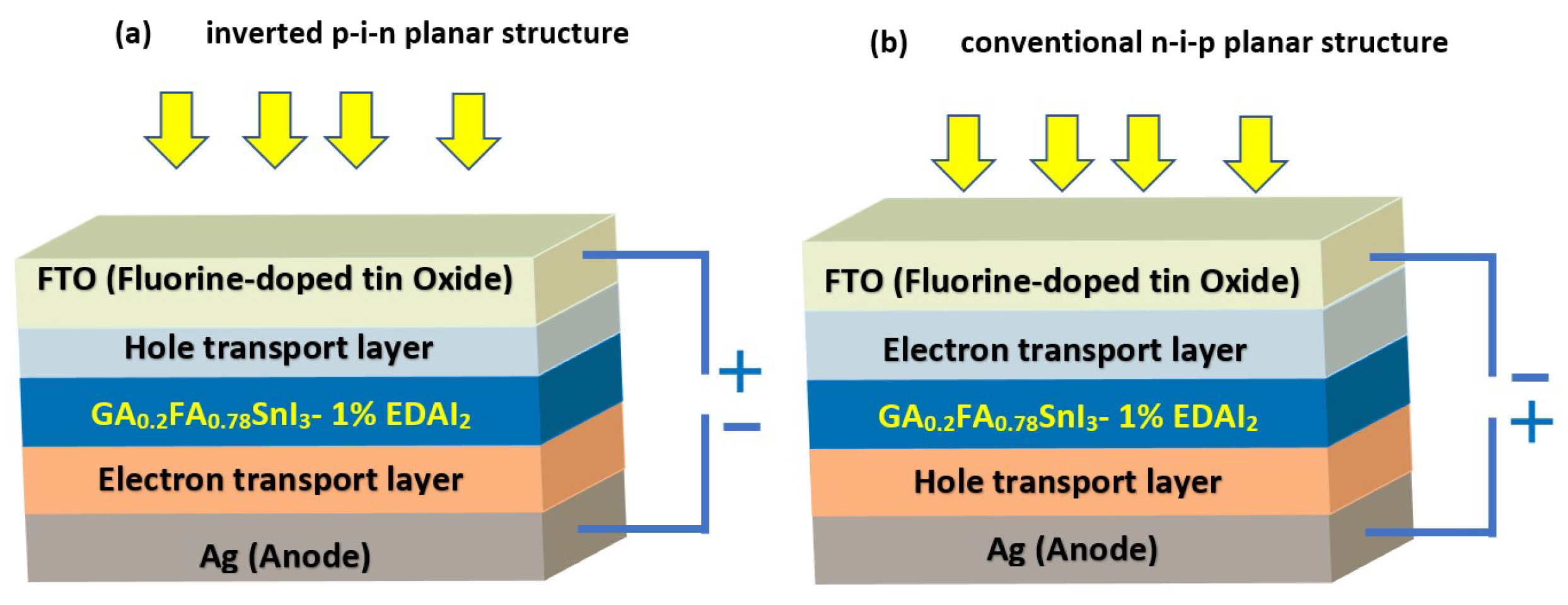
Figure 2 represent the J–V characteristics of the simulated inverted
p-
i-
n structure and its comparison with its experimental analog, previously studied in [
40] (red and blue curves, respectively), along with the curve of the
n-
i-
p structure herein simulated (black curve).
Although they both have a similar V, it can be noticed that the conventional n-i-p structure exhibits an offset in the J when compared with the inverted p-i-n one. In fact, the J behavior is dominated by the bandgap of the ETL: the higher the bandgap is, the better is the J performance. In our case, the bandgap of ETL-C60 (1.7 eV) is lower than that of the HTL-PEDOT:PSS (2.2 eV) considered for the p-i-n structure. This low bandgap causes a high absorption of the light in the ETL prior to its arrival at the absorber layer. As a consequence, less light reaches the absorber, causing a decrease in the J.
To confirm this finding, the quantum efficiency was calculated for each tested HTL material with C60 as ETL, and is illustrated in
Figure 3.
From
Figure 3, for the inverted structure, a difference in the quantum efficiency behavior was attributed to the difference in HTL materials. It is worth mentioning, that the curve corresponding to Cu
O is overlapping with that of PEDOT:PSS. It is evident that only when the light wavelength exceeds 570 nm, all four HTLs exhibit identical quantum efficiency characteristics. However, at lower wavelengths, it becomes apparent that CuI and CuSCN, which possess higher transparency, display superior quantum efficiency. The similarity in the behavior of the CuI and CuSCN curves can be attributed to their identical bandgap energy. Both materials have a bandgap of 3.4 eV, leading to their parallel response.
Additionally, in
Figure 4, representing the J–V characteristic of the PSC for each HTL material, it can be observed that the short-circuit current density (J
) of CuSCN and CuI reaches its highest value. This is primarily due to the large bandgap of these materials, which is advantageous for increased transparency to visible light in the HTL. When the bandgap of the HTL exceeds 2.9 eV, it exhibits enhanced transparency to visible light. Consequently, a greater amount of light can penetrate the perovskite layer and be absorbed, resulting in the generation of a higher number of electrons. On the other hand, in the case of the conventional structure, the choice of hole transport layer (HTL) material appears to have a minimal impact on the quantum efficiency (QE) and short-circuit current density (J
). This is because, in the case of the conventional PSC structure, light primarily enters the device through the electron transport layer (ETL), and the QE and J
are mainly influenced by the bandgap of the ETL, rather than that of the HTL. The only parameter that significantly affects J
in conventional perovskite solar cells is the conductivity of the HTL material. Higher conductivity of the HTL leads to higher J
values. Therefore, the conventional structure with CuI as the HTL demonstrates the highest J
, attributable to its superior conductivity. The major discrepancy in J
between the simulated devices with the conventional structure and the inverted structure can be attributed to the use of C60 as the ETL in the conventional structure, through which the light enters. The bandgap of the ETL material in the conventional structure is relatively low (1.7 eV, resulting in more light being absorbed by the ETL and less light being absorbed by the perovskite layer. Consequently, fewer electrons are generated, leading to significantly lower J
values in the conventional structure compared with the inverted one. Additionally, and for the same previously mentioned reason [
40], it is noteworthy that PSCs having CuI as the HTL exhibit the highest V
among all the tested solar cells with different HTL materials. This observation can be attributed to the presence of a negative valence band offset (VBO) at the HTL/absorber interface. This negative VBO leads to the formation of a barrier, promoting a more efficient electron–hole recombination process. Consequently, the V
, as well as other performance metrics such as J
, fill factor (FF), and power conversion efficiency (PCE), show a monotonic decrease. Conversely, when the VBO is positive and less than or equal to 0.3 eV (as is the case with CuI), excellent current–voltage (J–V) characteristics are obtained. The positive VBO facilitates a favorable charge transfer process, reducing electron–hole recombination and resulting in an improved J–V performance. Therefore, the utilization of CuI as the HTL material in PSCs proves beneficial, as it leads to the highest photovoltaic outputs and favorable J–V characteristics. These findings underscore the importance of the HTL material selection and its impact on the device’s performance. In summary, in the conventional structure, the HTL material has minimal influence on the QE and J
, with the conductivity being the primary factor affecting J
. The difference in J
between the conventional and inverted structures is primarily due to the lower bandgap and higher light absorption of the ETL material in the conventional structure.
3.1.1. Impact of HTL Thickness
The thickness of the HTL was fixed on 100 nm in the previously presented results. It has been found that the HTL thickness could impact the PSC performance [
61,
66]. The HTL thickness should be carefully chosen: on the one hand, this layer needs to be thick enough to completely cover the absorber layer, and, on the other hand, it needs to be thin enough to reduce the recombination rate. In fact, the electron–hole recombination depends on the path length of charge carriers. Moreover, it has been found that the electric resistance of the device, directly influencing the resistance of the layer, can also play a major role in predicting the recombination rates. Therefore, it is very important to perform a study in order to determine the optimal HTL thickness.
Figure 5 describes the evolution of the parameters of the PSC (PCE, V
, J
, and FF) with respect to the thickness of HTL materials.
From
Figure 5, it can be inferred that CuI exhibits a better PSC performance among the considered HTLs in the study. In addition to recording the best performance among the tested HTLs in this simulation study, CuI has been found to protect the HTL/perovskite interface from degradation, thereby improving the stability of the cell [
67]. Furthermore, another study confirms that the PSCs with CuI exhibit good long-term stability in the ambient atmosphere, attributed to the hydrophobic nature of CuI as an HTL. These results highlight the potential of CuI, fabricated using a simple and low-temperature processing method presented here, as a promising low-cost alternative HTL material for the future development of efficient and stable inverted planar PSCs [
68]. However,
Figure 5 shows that the thickness of the HTL does not affect any of the photovoltaic properties. This behavior is due to the fact that the light is entering from the ETL side, hence the thickness of ETL material is expected to have more effect on the PSC photovoltaic properties.
In the previous study on the inverted structure [
40], it was observed that the performance of the PSC decreased as the thickness of the hole transport layer (HTL) increased. This decrease was attributed to the reduction in conductivity of the Cu
O and PEDOT:PSS layers, as well as the increased light absorption by these HTL materials with lower bandgaps. However, in the current
n-
i-
p structure, where light enters from the electron transport layer (ETL) side, the thickness of the HTL does not affect the light absorption by either the HTL or the perovskite layer. Consequently, it does not significantly impact the overall performance of the cell. Furthermore, it is worth noting that the J
values for the most efficient PSC with the conventional structure are lower than those obtained for the least efficient and thicker PSC with the inverted structure. This indicates that the number of generated electrons in the conventional structure is already at its lowest. Therefore, increasing the thickness of the HTL and subsequently reducing its conductivity has little to no effect on the overall performance of the PSC. In conclusion, the impact of the HTL thickness on PSC performance differs between the inverted and conventional structures. While it plays a significant role in the inverted structure, it has minimal influence on the performance of the PSC with the current
n-
i-
p structure.
3.1.2. Impact of HTL Doping Concentration
In the previous section, the focus was on identifying the adequate HTL material along with its suitable thickness. Moreover, it is also necessary to determine the equivalent acceptor doping concentration (N
). A value of
cm
was assigned to (N
) in
Section 3.1.1. In this part, the objective is to find the optimal value of N
for the CuI material.
Therefore, N
was changed from
to
cm
, while studying its impact on the current density–voltage characteristics. The results of this study are plotted in
Figure 6.
The doping concentration of an HTL material enhances its conductivity and therefore has a positive impact on the efficiency of the PSC.
Figure 6 proves that the increasing of the doping concentration from
cm
to
cm
causes a rise of approximately 4 mA·cm
in the J
values due to an increase in the conductivity. Similarly, this also causes an increase in the PCE from
to
, mainly due to the decrease in the recombination rate. It is worth mentioning here that, in the previous study on the inverted structure [
40], it was found that the doping concentration had a limited impact on the solar cell performance. This was attributed to the fact that the increase of the fill factor, caused by the increase of the HTL doping concentration, is limited to a certain upper value; this latter value is due to a saturation in the sheet resistance of the HTL. Moreover, this maximum can be due to a saturation in the conductivity of the HTL [
69,
70].
In the work herein, since this latter limit was not attained, a major effect of the HTL doping concentration was obtained. As a conclusion, an optimal HTL doping concentration of cm was considered as a compromise between the fabrication cost and the enhanced PCE value of , slightly less than that obtained at cm ().
3.2. The ETL Material Impact on the Solar Cell Performance
Choosing a proper HTL material is indeed important, but also the adequate selection of the ETL material is necessary.
In this section, four ETL materials (TiO
, WS
, SnO
, and ZnOS) and four HTL materials (PEDOT:PSS, Cu
O, CuSCN, and CuI) were considered with all possible combinations, while the doping concentration was maintained at
cm
. The effect of the HTL/ETL combination on the J–V curve is schematized in
Figure 7.
Figure 7 demonstrates that the photovoltaic device with CuI as the HTL outperforms the devices with other HTL materials. This trend is evident across all the graphs, where the green color consistently exhibits the highest value of the J
. This outcome is further confirmed by the power PCE results shown in
Figure 8. The discrepancy arises primarily from the superior conductivity of the devices with the CuI HTL, which leads to a larger J
and thus an improved PCE. Notably, this disparity is even more pronounced when the devices are combined with SnO
and ZnOS as ETL materials. These two ETLs possess higher light transparency, resulting in an increased generation of electrons. Consequently, the difference in conductivity becomes more significant, indicating that the higher conductivity of the HTL correlates with a better J
value.
In the previous work, where the structure was inverted [
40], it was found that WS
induced a better performance than TiO
. In fact, they had close CBO values (
and −0.3 eV, respectively) and electron affinity (
and −4 eV, respectively). However, WS
had better permittivity, which ultimately caused a difference of
in the PCE. In the current study on the conventional
n-
i-
p structure, adopting SnO
and ZnOS as ETL materials led to the best performance, as can be seen in
Figure 7 and
Figure 8. More precisely, with ZnOs as the ETL, best performances are obtained, regardless of the HTL (highest J
and V
values). Although SnO
has better transparency to visible light since its bandgap is 3.6 eV, exceeding that of ZnOS of 2.83 eV; it appears that the counter impact of CBO and permittivity has more effect on the overall performance. Therefore, ZnOs is found to be the best ETL material in this study.
Ultimately, the HTL/ETL of CuI/ZnOS outperforms all other combinations, where the scored values are at their highest, with J = 19.5 mA·cm, V = 0.95 V, and PCE = 14.6%.
This latter finding is confirmed through the quantum efficiency represented in
Figure 9, where the CuI HTL was selected and tested with all other ETLs.
From
Figure 9, it can be noticed that WS
and C60 exhibit the lowest performance, due to their high light absorption (less light reaching the absorber layer). Moreover, ZnOs is found to overtake the other HTLs for the majority of the light spectrum [
71].
As a conclusion to this part, for the remainder of the study, CuI and ZnOS were adopted as the HTL and ETL, respectively.
3.2.1. Impact of ETL Thickness
In the above sections, a thickness of 50 nm was adopted for all the conducted studies. In this part, the impact of the thickness of the ETL on the efficiency of the photovoltaic cell is explored.
Figure 10 shows the effect of the ETL ZnOS thickness on the J–V characteristics and the power conversion efficiency. According to the latter figure, while V
remains constant, J
and PCE slightly decrease with the thickness.
In fact, when the ETL thickness increases, more light will be absorbed and therefore less light will reach the absorber. According to [
72], increasing the ETL thickness leads to larger pinholes forming, causing a deterioration in the J
.
Also, when increasing the ETL thickness, the electron–hole recombination increases, resulting in a rise in the resistance, indicated by the decreasing of J
. Consequently, this will cause a
drop in the PCE. To complement the latter conclusion, the impact of the ZnOS ETL thickness on the PSC quantum efficiency was conducted; the obtained results are plotted in
Figure 11.
At small wavelengths, light is susceptible to being absorbed by the ETL; therefore, its thickness will play a major role in determining the quantum efficiency. As shown in
Figure 11, the higher the thickne isss, the lower is the quantum efficiency. Conversely, ETL materials are transparent to light of high wavelengths, regardless of thickness.
Thus, the optimal thickness for the ETL is found to be 20 nm, scoring the best photovoltaic properties.
3.2.2. Impact of ETL Doping Concentration
Although determining the adequate ETL material (ZnOS) as well as its optimal thickness (20 nm) are of high importance, the doping concentration (N) of the ETL material is also crucial. N could impact both the J and the PCE. In all of the above sections, the ETL doping concentration was chosen to be N = cm for all the considered materials and thicknesses. In this section, the effect of the ZnOS doping concentration on the J and PCE is investigated.
Figure 12 depicts the effect of the doping concentration of the ETL ZnOS on the current density–voltage characteristics and the PCE of the PSC, where N
is varied from
to
cm
.
The latter figure shows clearly that the increase of N
leads to a rise in the J–V characteristic, accompanied by a rise in the PCE, indicating an improvement in the PSC efficiency. Actually, an increase in the doping concentration of the ETL causes a rise in the electron conductivity and a drop in the resistivity of the ETL. Moreover, in a previous work carried out by Xu et al. [
73], it was found that a high doping concentration of the ETL produces deep energy levels at the heterojunction interfaces, reducing the non-radiative recombination at the interface and enhancing the cell performance. Moreover, a large electric field is produced at high doping concentrations, effectively collecting the electrons and repelling the minority carriers away from the ETL/perovskite interface, thus diminishing interface recombination rates [
73].
Figure 12 shows that the highest values of N
=
and N
=
cm
generate the best performance (with respect to the PCE and J
). In addition, for these two doping concentrations, it can be noticed from the figure that the J–V curves are overlapped, and the PCE values are identical. Taking into consideration that a significant doping concentration of the ETL, of
cm
and more, is complex in terms of fabrication [
47], the optimal ETL doping concentration is proposed to be
cm
.


