Article

Evolutions of the Microstructure and Properties of the (CrMoNbTaZr)NX Films Prepared by Reactive Magnetron Sputtering: Effects of Stoichiometry and Crystallinity

1
Fujian Provincial Key Laboratory of Advanced Materials Processing and Application, Fujian University of Technology, Fuzhou 350118, China
2
Fujian Acetron New Materials Co., Ltd., Fuzhou 350209, China
3
Institute of Industry and Equipment Technology, Hefei University of Technology, Hefei 230009, China
*
Authors to whom correspondence should be addressed.
Coatings 2023, 13(8), 1424; https://doi.org/10.3390/coatings13081424
Submission received: 20 July 2023 / Revised: 1 August 2023 / Accepted: 7 August 2023 / Published: 14 August 2023

Abstract

:
(CrMoNbTaZr)NX coatings were deposited on Si (100) by magnetron sputtering under various N2/(Ar+N2) flow ratios. An X-ray diffractometer, transmission electron microscopy, scanning electron microscopy and atomic force microscopy were used to characterize the crystallinity and microstructure of the films. The elemental composition was characterized by energy dispersive spectroscopy and X-ray photoelectron spectroscopy. The hardness and friction coefficient were respectively determined by nanoindentation and nanoscratch. The sheet resistance was studied using a four-point probe. The results suggest that the crystallinity is strongly influenced by the nitrogen content in the films. The chemical stoichiometry of nitride determines the evolutions of the microstructure, mechanical properties and resistivity. Correlations between the microstructure and the properties of the (CrMoNbTaZr)NX films were studied.

Graphical Abstract

1. Introduction

The concept of high-entropy alloy (HEA) is characterized by its principal elemental composition, with five to thirteen constituting elements in near equimolar ratios [1,2]. Due to the combinatorial mechanisms of the high-entropy effect, lattice distortion effect, cocktail effect and hysteretic diffusion effect, HEAs provide outstanding properties, such as excellent structural stability [3], high temperature strength [4], corrosion resistance [5,6] and anti-oxidation [7,8].
Similar to the excellent properties of HEAs, high-entropy nitride (HEANX) films have attracted extensive research interest in the past fifteen years [9,10]. HEANX films are generally divided into two categories according to the metal composition: (1) alloy of nitride-forming metals; (2) incorporation of FCC metals or non-metals into nitride-forming metals. The microstructure of HEANX films correlates with the type of HEA and nitrogen concentration. The alloy of nitride-forming metals generally presents a BCC type simple solid solution HEA. As nitrogen is introduced, it gradually changes into simple solid solution of HEAN in FCC [11,12]. The coexistence of HEA and HEAN results in grain refinement or amorphization [13]. The FCC metals or non-metals comprising HEA show a dual-phase structure or simple solid solution with severe lattice distortion [14]. FCC nitride crystallites frequently emerge and grow with the increasing content of nitrogen. The grain size can be fine or even amorphous due to multi-phase coexistence within a certain range of nitrogen concentration [15,16]. The amorphous HEANX is smooth and stable [15].
The mechanical properties of HEANX films are dependent on the metal composition, nitrogen concentration and crystallographic structure [17]. It is reported that HEANX shows superior hardness and oxidation resistance than compositional nitrides, which make it a good candidate in the application of mechanical and thermal protection [12,18,19].
In the field of large-scale integrated circuits, a barrier is deposited to prevent the diffusion of Cu and Si atoms. TaN monolayer and TaN/Ta bilayer are commonly employed as the diffusion barrier [20]. With the relentless scaling down of microelectronic devices, demand for new barriers with reduced thickness and enhanced barrier performance is further increased. The barrier is required to possess low resistivity, high thermal stability, excellent density, smoothness and good adhesion. Amorphous thin films have received attention due to reduced surface roughness [21,22,23].
HEANX thin films show great prospects as a barrier in the Cu/Si interconnection [24,25]. As the Gibbs free energy of an alloy system decreases with the number of compositions, the high mixing entropy enhances the thermal stability of HEANX films [2,21]. Hsiao et al. reported a 1.5 nm VNbMoTaW thin film self-formed by segregation onto the Cu/Si interface from Cu coating, which was prepared by co-sputtering the HEA and Cu targets [26]. Chang and Chen reported the preparation of an (AlCrTaTiZr)N/(AlCrTaTiZr)N0.7 bilayer structured film, which was thermally stable at 900 °C [27].
Refractory metals are favored compositions for barrier coatings, due to their chemical immiscibility with respect to copper. Additionally, as refractory metal nitrides are conductive or semi-conductive [19], they greatly extend the composition window for developing optimized barrier coatings. In the composition window, the parameters include not only the composition and concentration of metals, but also the incorporation of nitrogen. Among them, magnetron sputtering is the most popular technique due to the advantage of preparing films with excellent surface smoothness, good substrate adhesion, as well as tunable composition and microstructure [27,28].
The microstructure of refractory HEANX films has been well studied. The crystal structure of HEA films can be polycrystalline, nanocrystalline or amorphous, depending largely on the atomic radius difference of the refractory metals [29,30,31,32]. The stoichiometric HEAN often possesses good FCC nitride crystallites. Various crystallographic structure for the under-stoichiometric HEAN were reported, from amorphous to fine-sized crystallites, because of the combined phases of HEA and HEAN [18,33,34,35]. On the contrary, few studies have illustrated how the composition determines the evolution of mechanical properties and electricity. In fact, the properties are highly dependent on the evolving microstructure. So far, it has not been possible to draw a relationship between the microstructure and performance of HEANX films, which is of key importance to optimize or guide the optimization of the compositions.
In this study, a series of (CrMoNbTaZr)NX films, with varying N concentrations from pure HEA to chemically over-stoichiometric nitride, were prepared by reactive magnetron sputtering. Equal-mole metal contents were used in each film. The effects of N content on the microstructure, electrical properties and nanomechanical properties of the (CrMoNbTaZr)NX films were studied.

2. Materials and Methods

2.1. Film Preparation

(CrMoNbTaZr)NX coatings were deposited on polished Si (100) wafers using a JGP450A2 magnetron sputtering tool (Sky Technology Development, Shenyang, China) under various N2/(Ar+N2) flow ratios (RN). The commercial Cr and MoNbTaZr alloy plates, both Ø 50 mm × 5 mm in size and >99.7% purity, were used as targets. The deposition tool was the same as described in the literature [36]. The targets were made by powder metallurgy, and the alloy plate possessed equal-mole metals. The targets were placed in the bottom part of the deposition chamber and faced the center of the substrate holder at an equal distance of 8 cm, in which the Si substrate with a size of 20 × 20 mm2 was placed. Before mounting on the holder, the Si was ultrasonically cleaned in ethanol and then dried by pure N2 flow. Prior to deposition, the chamber was evacuated to a base pressure of 8×10⁻⁴ Pa, then Ar (99.99%) flow of 40 sccm was introduced. The substrate holder was rotated at 2 rpm, and the substrate temperature was kept at 300 °C.
Table 1 shows the processes and parameters during film deposition. Target sputter cleaning was carried out for 10 min to remove the surface impurities, while the substrate was shielded. After that, a constant nitrogen flow that met the given RN was introduced to deposit an adhesion layer on the substrate. The adhesion layer was deposited for 5 min, and during this period, the substrate bias linearly descended from the initial −600 V to −120 V. Then, the top layer was deposited at −120 V for 120 min. Seven films were prepared with various RN of 0, 0.1, 0.2, 0.3, 0.4, 0.5 and 0.6.

2.2. Microstructure Characterization

The plane-view and cross-sectional morphology of the films was observed by field emission scanning electron microscopy (SEM, FEI NovaNanosEM450, Columbia, MD, USA), operating at 2–10 kV by secondary electron. Deposition rate was derived from the SEM result of the film thickness. Smoothness of the films was characterized using atomic force microscopy (AFM, Bruker Dimension Icon, Karlsruhe, Germany) under the non-contact mode, the RMS surface roughness was derived from the AFM image.
The elemental composition of the (CrMoNbTaZr)NX coatings were determined by energy-dispersive X-ray spectrometry (EDS, Oxford Instruments X-Max, Oxford, UK), which was coupled with the aforementioned SEM. The composition was characterized by an EDS mapping scan of a 60× 80 μm2 area. For each sample, the average composition was based on five different areas. The film chemistry was determined with an X-ray photoelectron spectroscopy analysis (XPS, Thermo Scientific ESCALAB 250, Waltham, MA, USA). The photoelectron spectra were excited with a monochromatic Al Kα radiation (1486.7 eV) and the binding energy of the atomic level was calibrated with the C 1s peak at 284.6 eV. To eliminate the surface contaminants, the specimen was sputtered with 3 keV Ar+ ions for 3 min. To characterize the chemical states of the elements, a wide scan was performed with a passing energy of 80 eV for 10 min. The core-level spectra of the elements in the studied films, including Cr 2p, Mo 3d, Nb 3d, Ta 4f, Zr 3d, O1s, N1s and C1s, were scanned at a passing energy of 40 eV for 5 min.
Phase composition of the (CrMoNbTaZr)NX films was characterized by X-ray diffractometry (D8 Advance, Karlsruhe, Germany) using Cu Kα radiation and a nickel filter with a Bragg–Bretano geometry. The samples were scanned from 20° to 80° with a resolution of 0.02° per step and a step time of 0.3 s. The microstructure of the films was studied using a transmission electron microscope (TEM, JEOL JEM-2100, Tokyo, Japan). The TEM samples were prepared by a focused ion beam (FIB, FEI Gatan691, Columbia, MD, USA) with an omni-probe pick-up system.

2.3. Properties’ Characterization

The hardness and Young’s modulus of the films were measured by a nanoindentation system (Hysitron TI Premier, Karlsruhe, Germany) with a Berkovich indenter (nominal radius: 25 μm). The penetration depth of the indenter was set at 105 nm, which is less than 1/10 of the film thickness. Nine indentations were made to achieve their average for each specimen. The friction coefficient of the film was measured at room temperature by a nanoscratch system (Hysitron TI Premier) with a spherical indenter. The measurement parameters were as follows: applied load 5 mN, constant sliding speed 1 μm/min for 10 min. The electrical resistivities of the films were determined by measuring the sheet resistances of the films using a four-point probe (RTS-9, Guangzhou, China). The average resistivity was based on 5 effective results for each sample.

3. Results and Discussion

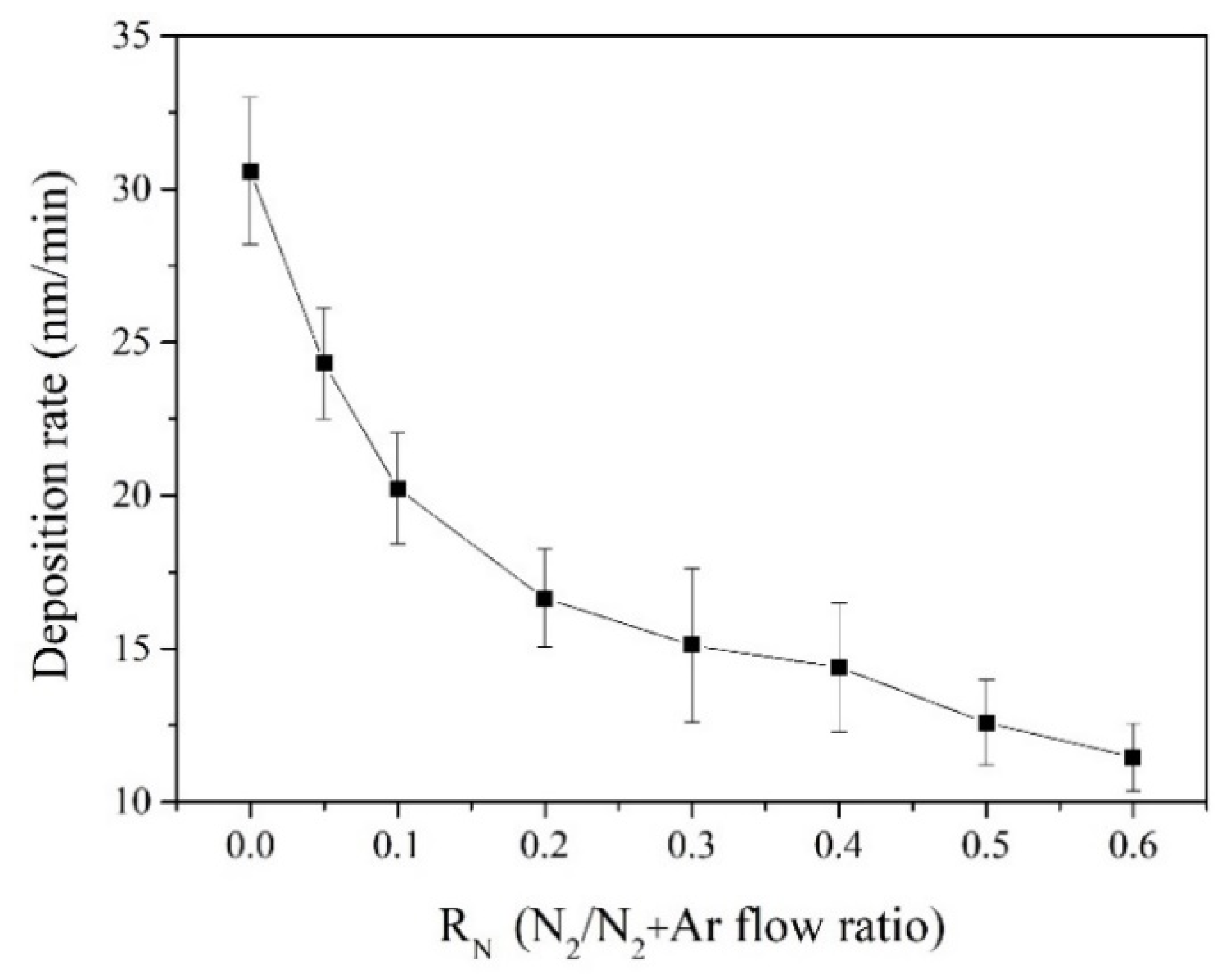
3.1. Chemical Composition and Deposition Rate

Figure 1 shows the chemical composition of the films. Note that according to the EDS results, samples RN = 0.1, 0.2, 0.3 and 0.4 show oxygen concentration in the range 5.8 ± 2.6 at.%, while RN = 0, 0.5 and 0.6 possess 12.1, 21.9 and 23.0 at.% O, respectively. For better describing the stoichiometry of the nitride, oxygen was removed in Figure 1. At lower RN, N concentration in the films rises rapidly as RN increases. Samples RN = 0.1 and 0.3 possess 35 and 47 at.% N, respectively. As RN further increases from 0.4 to 0.6, the nitrogen concentration increases from 48.2 to 51.1 at.%. Samples with RN >= 0.4 are considered as a zone where N concentration is less sensitive to RN. A similar trend was revealed in other studies, in which the gradient of nitrogen increase slowed down when the composition reached the chemical stoichiometry of the transition metal nitride [35,37,38].
The transition metal nitrides commonly possess an FCC unit cell structure. Except for Mo2N, the nitrides of the compositional metals are NaCl type. As shown in Figure 1, the elemental percentages of metals are roughly stable as RN varies. The composition in the films meets the concept of HEA and high-entropy alloy nitride (HEAN). Supposing that the stoichiometric HEAN is a homogeneous solid solution of NaCl type, the N concentration can be theoretically estimated. Based on the metal concentration in each film, Figure 1 plots the estimated concentration of nitrogen in stoichiometry with a dashed line as a reference. The result reveals that the N concentration in sample RN = 0.3 already reached the stoichiometric nitride. However, the N content increases continuously against RN. There are two possible reasons for this. Firstly, the over-saturated N is incorporated into the grain lattice (of nitride) by means of ion bombardment during sputtering deposition; secondly, Ta3N5 and Nb3N4 with a larger N atomic percentage may be produced, as reported in the literature [39].
By measuring the thickness of the (CrMoNbTaZr)NX films deposited within an equal time of 120 min, the deposition rate is calculated and plotted in Figure 2. The largest deposition rate of 30.58 nm/min is obtained for the HEA film. It decreases sharply when N2 is introduced. It is acknowledged that the deposition rate of the metal nitrides is lower than that of the metals due to the decreased sputtering rate of the target species in a nitrogen-containing atmosphere [40,41]. As RN increases to 0.4, the ramp gradually decreases. However, the ramp rises when RN increases to 0.5 and 0.6. Sample RN = 0.6 possesses a deposition rate as low as 11.47 nm/min. In view of a higher O concentration and lower deposition rate, the film was prepared by a poisoned target when RN increased to 0.5.
Figure 3 shows the variation of XPS as a result of RN. The tested samples are RN = 0, 0.1, 0.3 and 0.5. The survey spectra of the tested films, as shown in Figure 3a, reveal not only the presence of all the compositional metals, but also the varying concentration of O and N in the films. According to these spectra, samples RN = 0, 0.1, 0.3 and 0.5 contain 16.1, 8.6, 6.4 and 26.2 at.% O, respectively. The oxygen content in the films obtained by XPS is higher than that of EDS, while the trends of variation of the oxygen content against RN are much the same. This is because XPS reveals the composition of the shallower surface of the films, and the surface of films, especially pure HEA, possesses strong oxygen adsorption. With the introduction of nitrogen, the surface energy of the film reduces and the concentration of adsorbed oxygen decreases. Consistent with EDS, XPS also reveals that the oxygen content drastically increases as RN increases to 0.5. This is probably due to the decrease in the deposition rate, which results in a relatively high oxygen content entering the film. During the deposition process, the residual oxygen in the chamber is incorporated into the growing film continuously. The oxygen content is low if the film is deposited at a high rate. As the deposition rate decreases, the oxygen content increases.
Narrow scans of core-level spectra of the elements are shown in Figure 3b–g. For each element, the standard binding energies in metal, nitride and other composite states are marked by the dashed lines. For instance, the Cr3d doublet comprises 2p3/2 and 2p1/2 spin-orbit split components at 574.1 and 583.4 eV, respectively. In pure HEA, Mo, Nb and Ta show simple metal states, while elements Cr and Zr also show the states of oxide.
Except for O incorporation, the binding state of the compositional metals roughly undergoes the transition process of metal, metal + nitride and nitride, corresponding to an increase in RN from 0 to 0.1 and 0.3, respectively. As shown in Figure 3d–f, sample RN = 0.1 shows that the shoulder peaks comprise metals and nitrides, while sample RN = 0.3 reveals pure nitride. The binding state of the compositions is consistent with the stoichiometry that is shown by EDS.
In sample RN = 0.5, the peaks of all the metals move towards higher binding energies. The peak positions shown in Figure 3d,f were reported as the binding state of NbON and ZrON [35,42]. In view of high oxygen content in the film, the increased binding energy for the metals in sample RN = 0.5 probably corresponds to the formation of oxynitride of all metals.

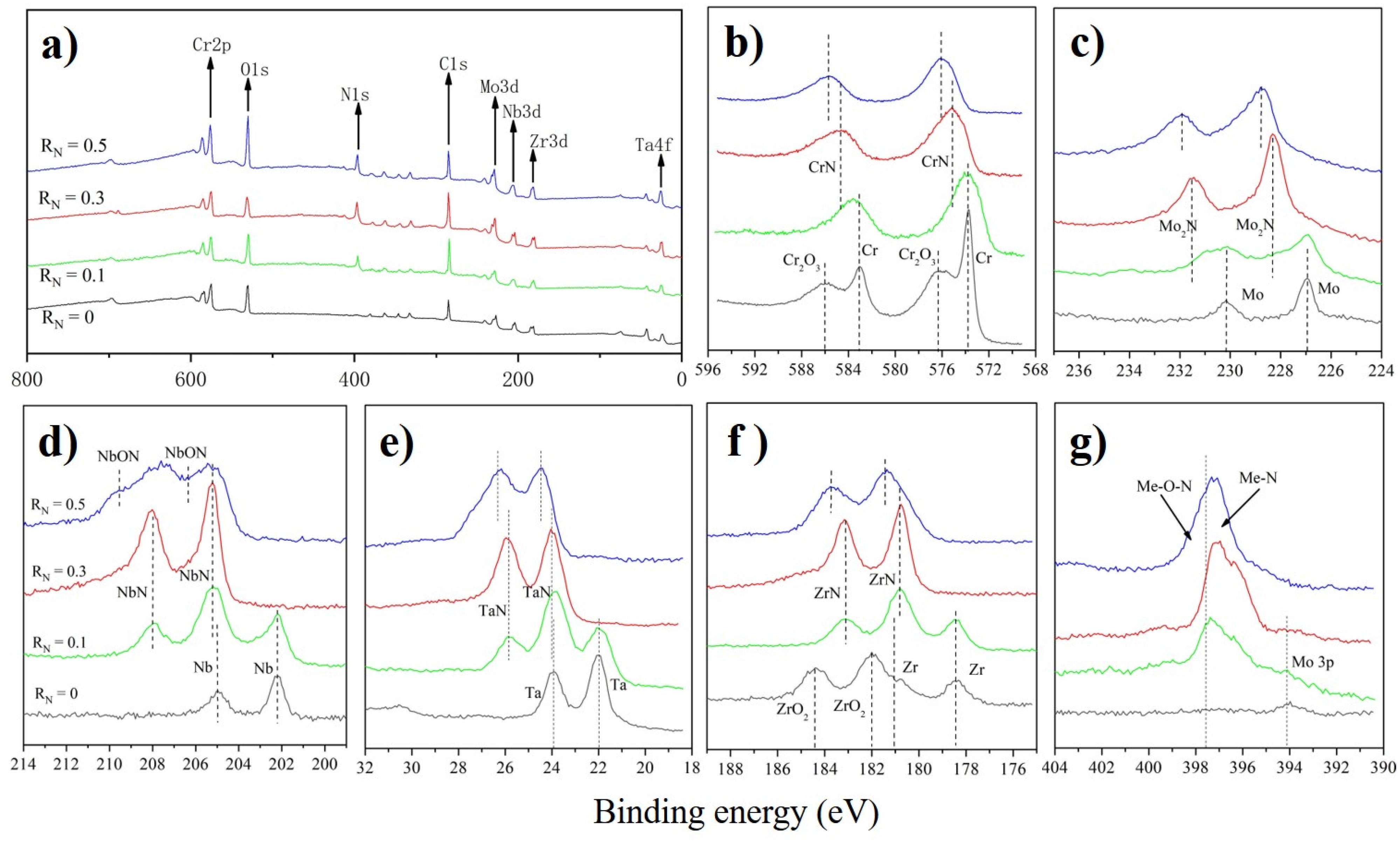
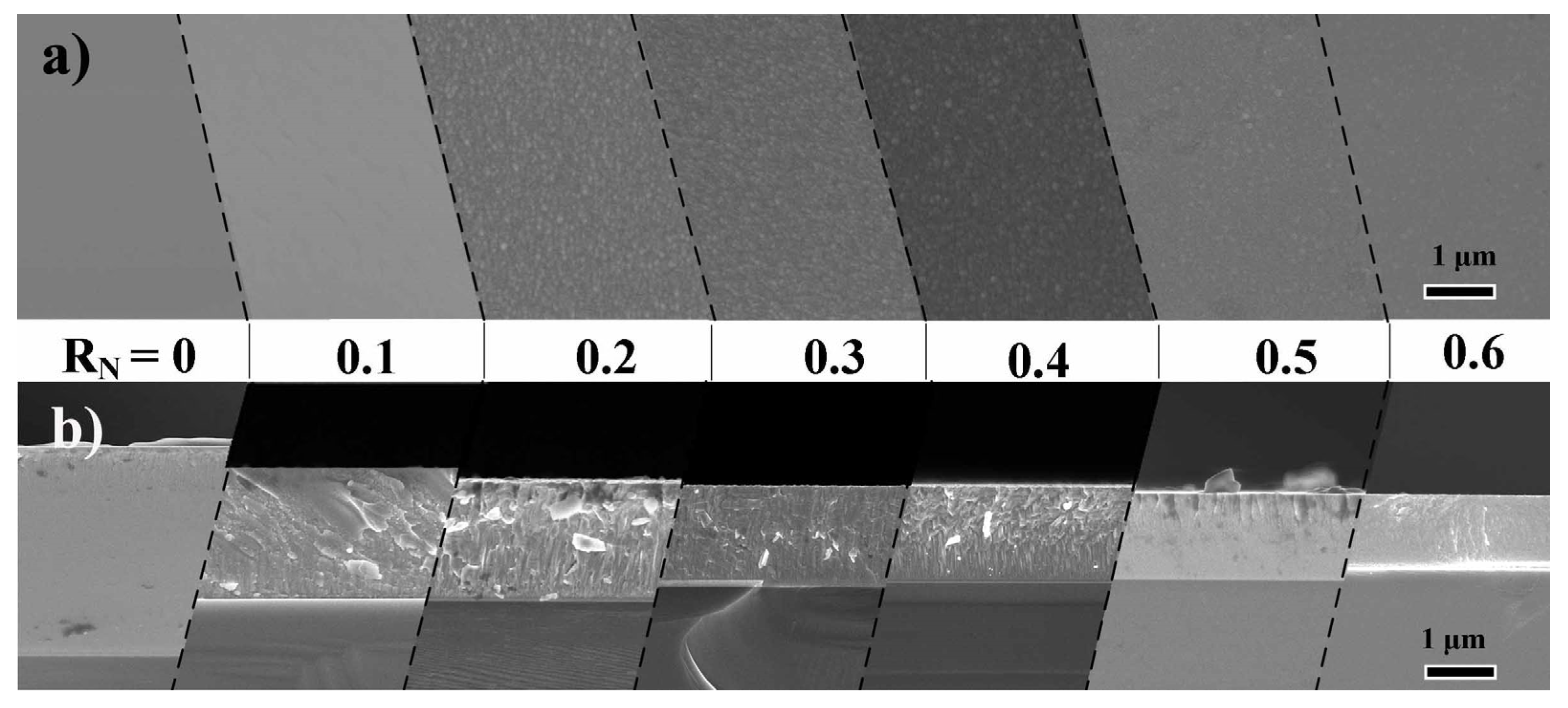
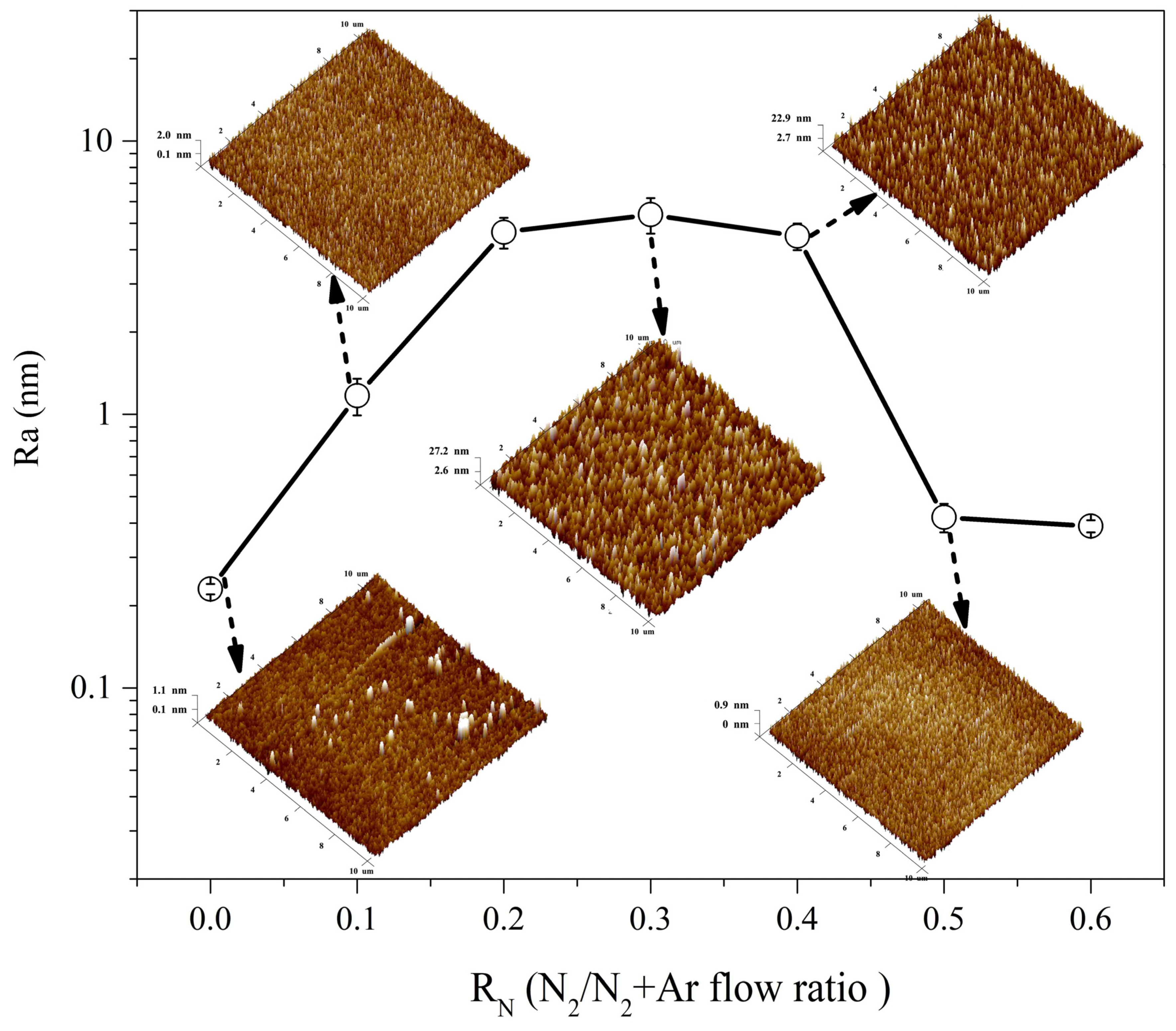
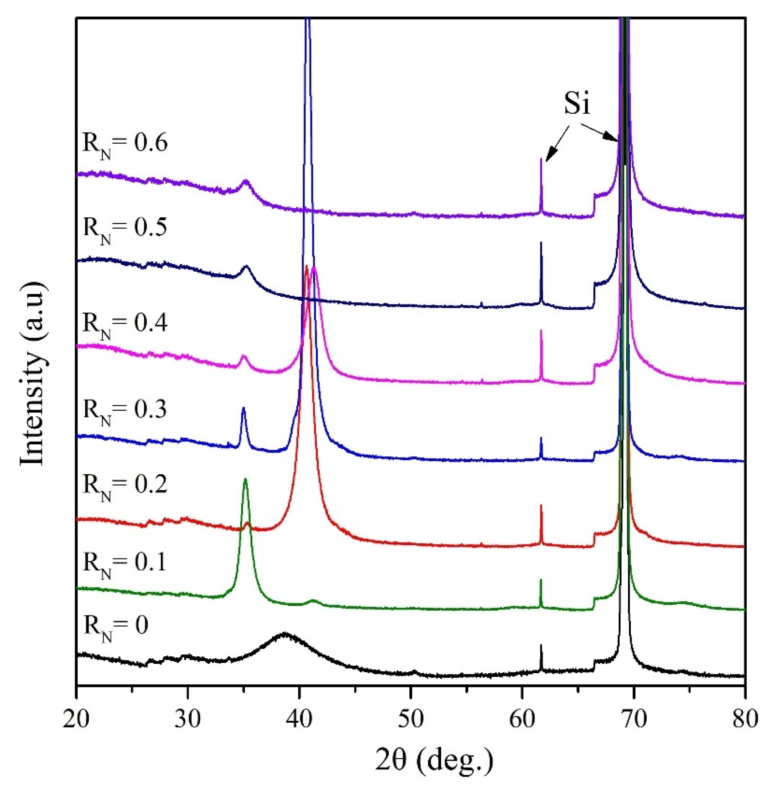
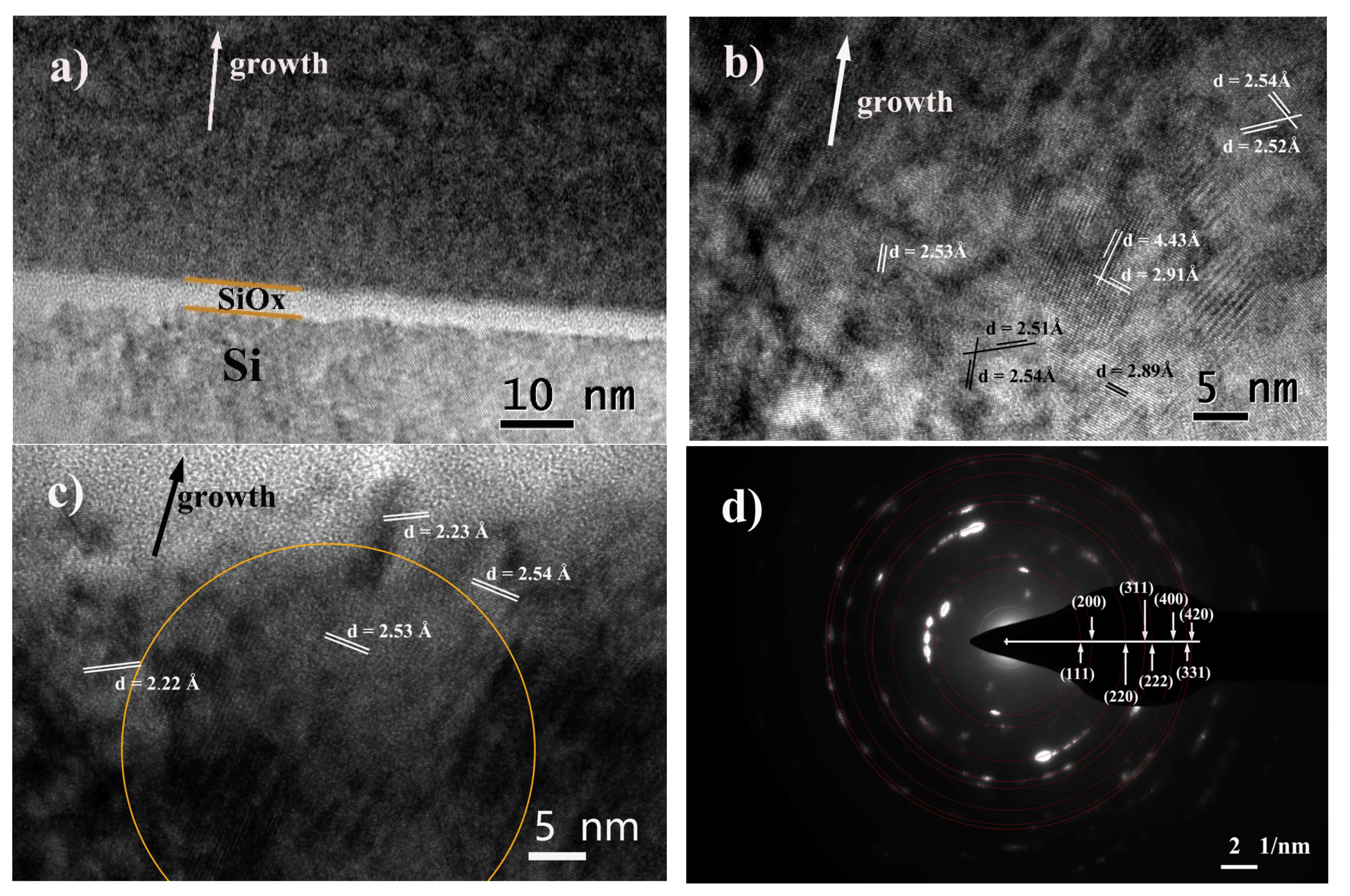
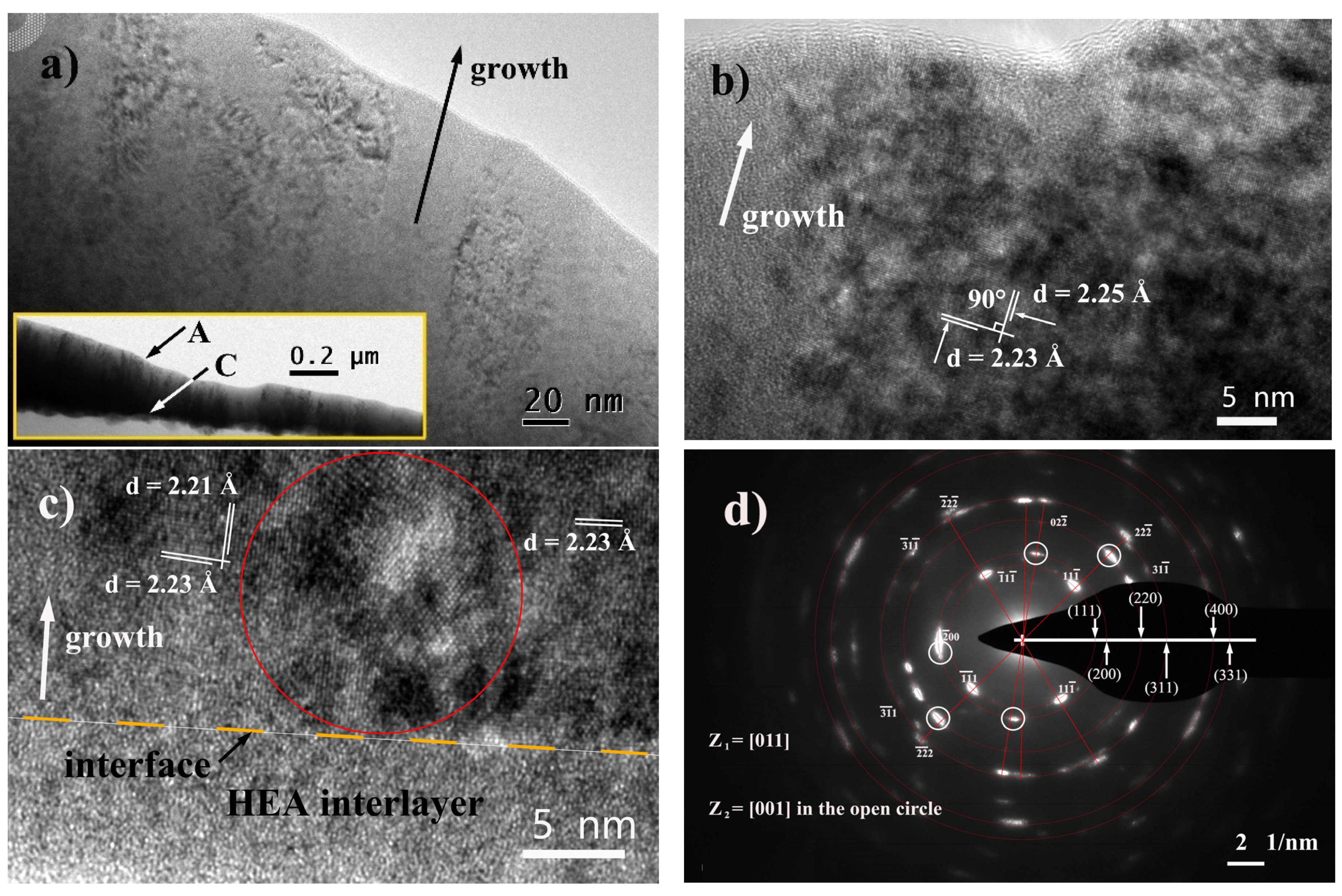
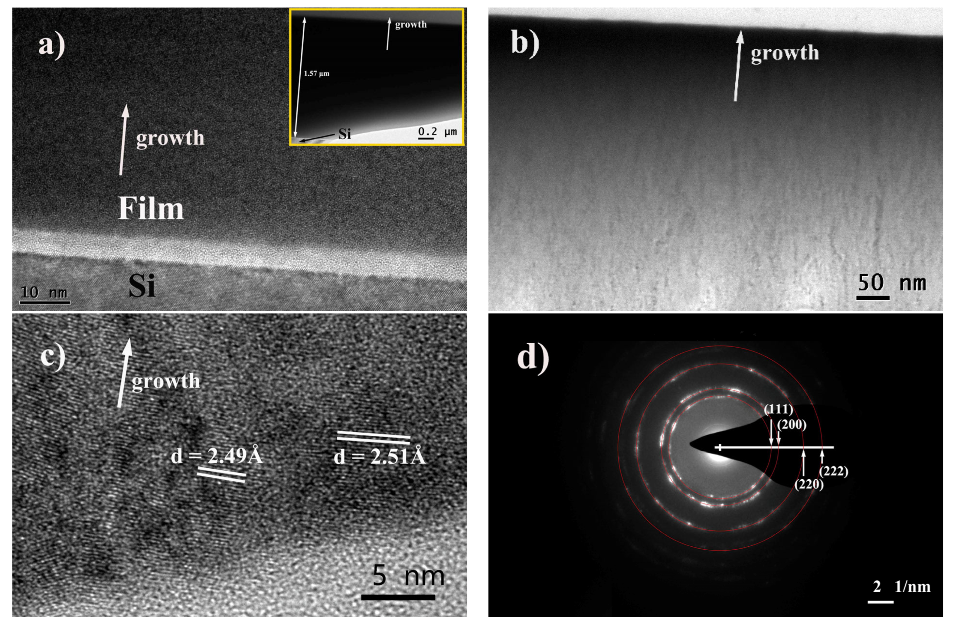
3.2. Microstructure and Crystallography

Figure 4 shows the SEM microstructure of the (CrMoNbTaZr)NX coatings. The plane-view morphology reveals that the films with RN less than 0.2 provide a smooth and featureless surface. As RN increases from 0.3 to 0.4, the surface of films becomes granular. As RN increases further, the size of the granule reduces and the surface returns to smooth.
As RN increases, the cross-sectional morphology varies. The films with RN ranging from 0 to 0.2 present smooth and featureless cross-sections, while the samples of RN = 0.3 and 0.4 are coarse and columnar-like. As RN increases to 0.5 and 0.6, the column feature diminishes. The fracture surface becomes dense and smooth.
Figure 5 plots the variation of the average surface roughness (Ra) against RN according to the AFM study. Pure HEA possesses Ra as low as 0.23 nm. The films firstly grow rougher with RN and reach the largest Ra of 5.38 nm for sample RN = 0.3. As RN increases further, the roughness decreases. Sample RN = 0.5 shows Ra down to 0.42 nm. Similar trends were reported in the literature [38].
Insets show some typical film morphologies illustrating the variation. Pure HEA presents a very flat surface with even surface granules having heights less than 1.1 nm. Sample RN = 0.1 shows that the height of surface particles slightly increases to 2.0 nm. The value of the peak–valley grows to 27.2 nm and 22.9 nm for samples of RN = 0.3 and 0.4, respectively. After that, it drastically reduces to 0.9 nm for RN = 0.5. The samples of RN > 0.3 show that not only the surface roughness but also the size of surface particles decrease with the increasing RN.
Figure 6 shows the XRD patterns of the (CrMoNbTaZr)NX films. The crystallographic structure of the films varies with RN. Pure HEA possesses a single broad peak at 38.72° representing an amorphous microstructure. Though the compositional metals are BCC type, the growth of homogeneous BCC solid solution HEA crystallites is inhibited by strong lattice distortion, due to the large atomic radius difference of the metals. A similar result was reported by Cui et al. [43]. Comparatively, Feng et al. have characterized well-crystallized BCC grains in their HEA film by magnetron sputtering of a mosaic CrMoNbTaV target without substrate heating [35]. As N2 is introduced, the crystallographic structure of (CrMoNbTaZr)NX emerges and evolves with the varying RN. Sample RN = 0.1 presents a dominant diffraction peak at 35.15° and a weak one at 41.22°. In contrast, sample RN = 0.2 shows a weak diffraction peak at 35.08°, and the diffraction at 41.28° becomes dominant.
It is acknowledged that the refractory HEA nitride films possess B1-structured nitride in solid solution [35]. The present (CrMoNbTaZr)NX films probably form a single solid solution nitride at its chemical stoichiometry. Hence, the theoretical cell parameter of CrMoNbTaZr and chemically stoichiometric (CrMoNbTaZr)N can be theoretically estimated by Vegard’s law, based on the composition of each film [12,44]. The estimated lattice constants of pure HEA in BCC and chemical stoichiometric (CrMoNbTaZr)N in the NaCl type are 3.223 Å and 4.321 ± 0.006 Å, respectively. Accordingly, the XRD peak position of sample RN = 0 corresponds to an average spacing of ~2.324 Å for d110 and gives the lattice constant a = 3.286 Å. This result reveals a lattice expansion compared with the estimation.
Based on the estimated lattice constant of the stoichiometric (CrMoNbTaZr)N in the NaCl type, the XRD pattern will show a diffraction of (111) and (200) at 2θ = 35.97° and 41.75°, respectively. Apparently, samples RN = 0.1 and 0.2, respectively, correspond to (111) and (200) preferential growth of the cubic HEAN grains.
Samples RN = 0.3 and 0.4 still possess (200) preferential growth. Sample RN = 0.3 shows very strong diffraction intensity that suggests good crystallization of the nitride. The diffraction intensity decreases in sample RN = 0.4. Additionally, the peak position of (200) slightly moves to 40.82° for RN = 0.3 and 40.77° for RN = 0.4.
As RN further increases, the diffraction intensity decreases drastically. Samples RN = 0.5 and 0.6 show nearly the same XRD pattern. Both of them possess only one weak peak at 35.28° corresponding to (111) diffraction of the cubic HEAN. The diffraction intensity reveals that the grain size in these films is strongly reduced.
The variation of crystallographic structure correlates with the chemical stoichiometry of the (CrMoNbTaZr)NX films. The stoichiometric HEAN deposited at RN = 0.3 shows the strongest XRD peak intensity. In the films with under-stoichiometric nitrogen content, the grain size of HEAN is limited by insufficient nitrogen content and lattice defects. As for RN > 0.3, the deposited N species surpasses the stoichiometric nitride and results in nitrogen being incorporated into the growing HEAN crystals. The over-stoichiometric nitride grows with lattice expansion, grain refinement, as well as the decrease in and broadening of the XRD peak. In samples RN = 0.5 and 0.6, the crystallization of cubic HEAN is drastically inhibited by incorporation of excess and ever-increased nitrogen and a large mass fraction of oxygen.
The nitrogen concentration influences the orientation of grains. As RN increases towards the formation of stoichiometric nitride, the preferential orientation of the nitride moves to (200). This is ascribed to a competitive growing mode driven by strain energy and surface energy [45]. The grains of chemically non-stoichiometric nitrides possess larger amounts of lattice distortion and higher strain energy than the stoichiometric nitride. Therefore, the cubic nitride grains in RN = 0.1 preferentially grow on (111), since the exposed lattice plane (111) exhibits the lowest surface energy. On the contrary, since stoichiometric nitride crystallizes with low strain energy, (200) texture appears because it grows faster compared with (111).
The microstructures of samples RN = 0.1, 0.3 and 0.5 were studied by TEM along the cross-section of the films. For each film, the high-resolution microstructure was examined by bright-field imaging. Figure 7 presents the microstructure of sample RN = 0.1. The microstructure of the HEA interlayer is shown in Figure 7a, which possesses a dense and homogeneous structure with very weak crystallization. As nitrogen is introduced (RN = 0.1), the crystallites emerge, as shown in Figure 7b. The grains preferentially exhibit a lattice spacing of about 2.52 Å, which correlates with (111) of the NaCl-type HEAN.
Figure 7c exhibits the microstructure of the film near the surface. In addition to the HEAN grains with (111) parallel to the film surface, there are grains with a lattice spacing of about 2.24 Å. According to the lattice morphologies of the latter, they correspond to the (110) plane of unexpected BCC metals rather than (200) of cubic HEAN. Considering that N concentration in the film is much lower than the chemical-stoichiometric nitride, the film probably contains the phases of metal or alloy. The grains of metal and nitride show a columnar structure towards the film surface. Most of the metal grains reveal a width of column not more than 5 nm, as shown in Figure 7c.
Figure 7d presents the selected-area electron diffraction (SAED) pattern of sample RN = 0.1, corresponding to the place marked with an open circle in Figure 7c. The pattern reveals that the diffraction of FCC nitride and BCC alloy overlaps. As marked by a series of concentric circles, the spacings d = 2.53 Å, 2.19 Å, 1.56 Å, 1.33 Å, 1.27 Å and 1.10 Å correspond with (111), (200), (220), (311), (222) and (400) of the NaCl-type HEAN, respectively. Meanwhile, the spacings of d = 2.19 Å, 1.56 Å, 1.27 Å and 1.10 Å also correspond with (110), (200), (211) and (220) of the BCC alloy, respectively. According to the SAED pattern, the lattice constants of the HEAN and alloy are a = 4.39 ± 0.01 Å and 3.11 ± 0.01 Å, respectively.
The sparsely distributed spots in the SAED pattern confirm that the number of grains is limited in the marked area, while the unevenly distributed intensity corroborates the preferential orientation of the grains. The ordered spots at d = 2.19 Å and long comet tail for d = 1.56 Å confirm the presence of preferential orientation and strain gradient in the growing grains.
Figure 8 shows the cross-sectional microstructure of sample RN = 0.3. The film had peeled from the substrate during the process of TEM sample preparation. The film exhibits a columnar structure, as shown in Figure 8a. The inset presents the structure of the film at lower magnification, in which arrow A marks the structure that is shown in Figure 8a. A high-magnification view of the grain of columns reveals a well-crystallized grain, as shown in Figure 8b. The lattice spacings of the crystal planes correlate well with (200) of the NaCl-type HEAN. The structure suggests that the grain of HEAN grows with <001> towards the surface. The grain size is much larger than that of sample RN = 0.1.
Figure 8c shows the microstructure of sample RN = 0.3 located at the interface between the HEA interlayer and HEAN top layer, as shown by arrow C in the inset of Figure 8a. An open circle marks the place where two grains overlap. As separated by the yellow dash line, the HEA is amorphous. The HEAN possesses good crystallization, in which the <001> preferential orientation dominates. Figure 8d shows the selected area electron diffraction (SAED) pattern of Figure 8c. According to the pattern, the labeled diffraction spots correspond to an axis z1 = [011] for the cubic HEAN. In addition, another axis z2 = [001] for HEAN is discovered with the spots marked by open circles. The SAED pattern suggests the existence of several grains with varying orientation at the beginning of deposition. The lattice planes derived from the spots show the lattice constant a = 4.46 ± 0.05 Å for the cubic HEAN.
Figure 9 reveals the cross-sectional microstructure of sample RN = 0.5. The bright-field image reveals a dense and featureless structure of the film, as shown in Figure 9a. The inset of Figure 9a guides the determination of the growing direction and thickness of the film. According to Figure 9a, the film is amorphous at the very beginning. The crystallization may emerge slowly and sparsely as the film grows. As shown by the darker contrast in Figure 9b, there are occasionally tiny grains near the film surface. The high-magnification microstructure shown in Figure 9c confirms that the grains of cubic nitride grow preferentially with <111> towards the film surface. However, the grain size is less than 3 nm along the direction parallel to the film surface. Figure 9d shows the SAED pattern of Figure 9b. The pattern suggests the film is composed predominantly of polycrystalline FCC nitrides, with a lattice constant a = 4.31 ± 0.01 Å.

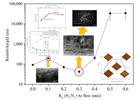
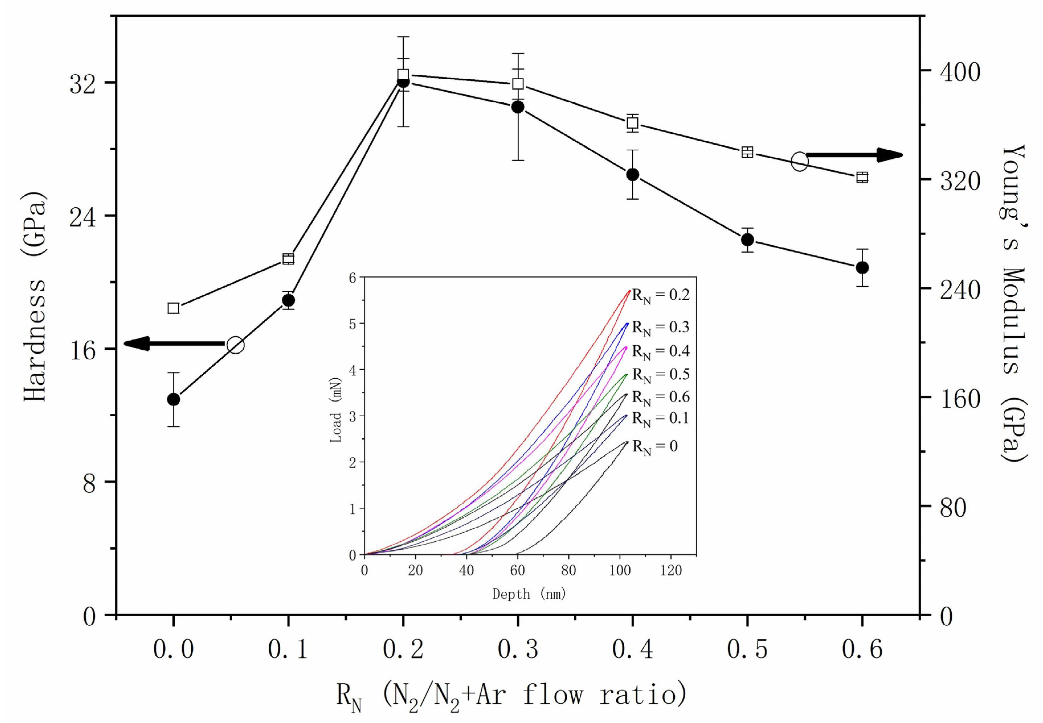
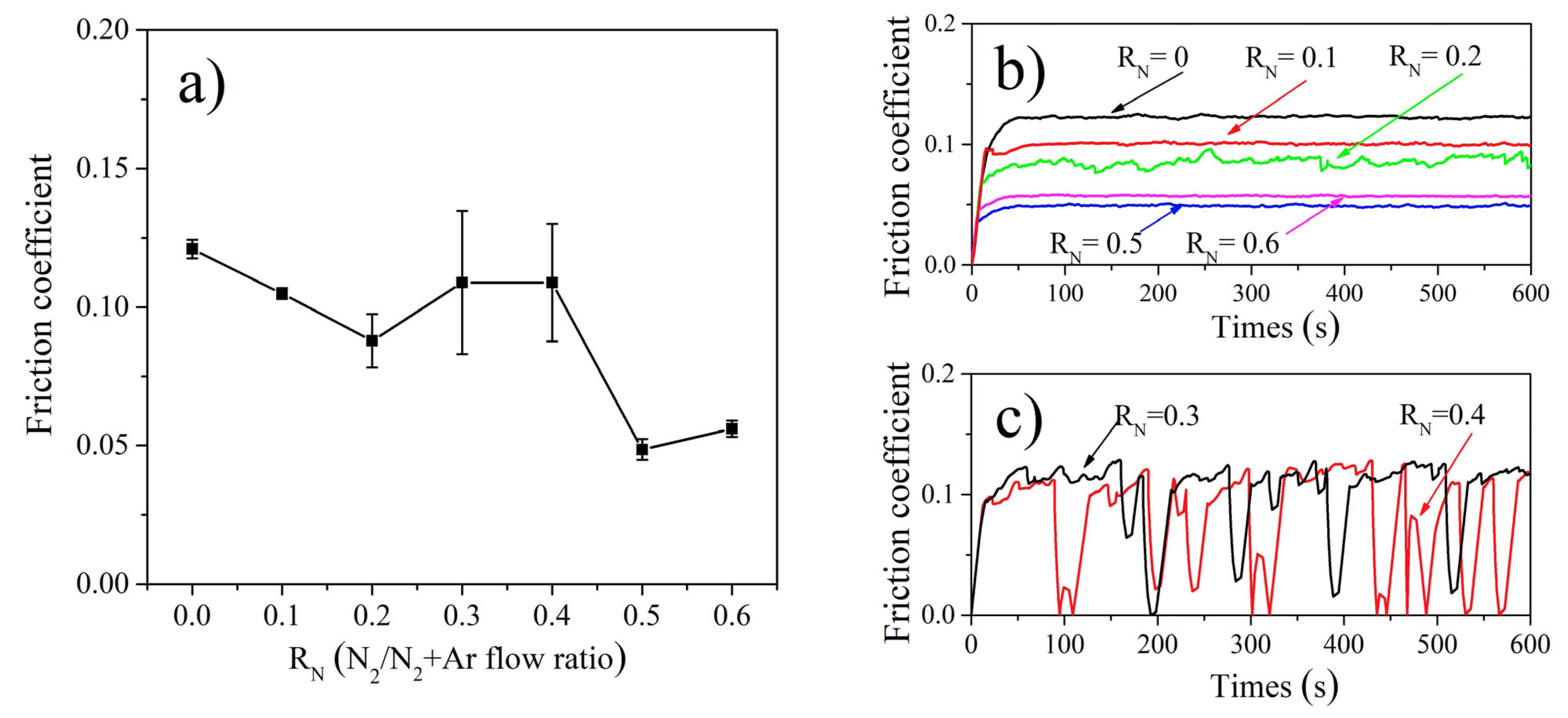
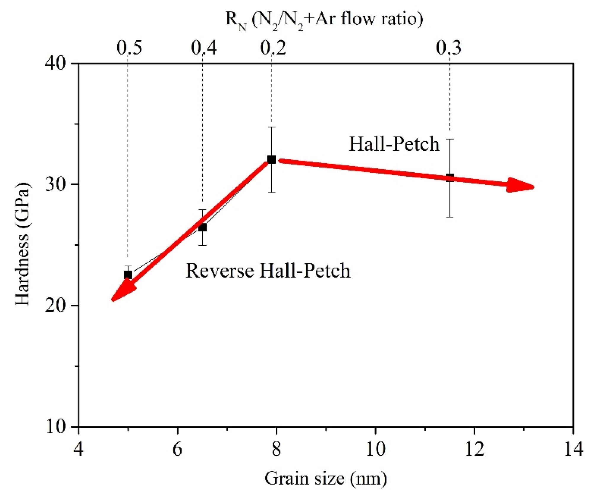
3.3. Mechanical and Electrical Properties

Figure 10 shows the hardness and Young’s modulus of the (CrMoNbTaZr)NX films deposited under various RN. Pure HEA film possesses relatively lower hardness and Young’s modulus at 12.9 ± 0.2 GPa and 225.2 ± 2.8 GPa, respectively. With the introduction of nitrogen, the hardness of RN = 0.1 increases to 18.9 ± 0.5 GPa. Sample RN = 0.2 drastically increases the hardness to the highest value of 32 ± 2.7 GPa. As RN further increases, the hardness decreases continuously. Samples RN = 0.5 and 0.6 possess the hardness of 22.5 ± 0.7 GPa and 20.9 ± 1.1 GPa, respectively. The varying trend of the Young’s modulus is the same as that of the hardness. Sample RN = 0.2 possesses the largest Young’s modulus of 396.8 ± 11.9 GPa, while that of sample RN = 0.6 reduces to 321.4 ± 2.2 GPa. The inset of Figure 10 plots the variation of load–displacement dependency of the films. At the same displacement of 100 nm, sample RN = 0.2 presents the largest indenting load and elastic recovery, while pure HEA shows the opposite result. The indentation resistance decreases with RN in the present (CrMoNbTaZr)NX films.
The hardness of the magnetron sputtering coatings of simple Cr, Mo, Nb, Ta, Zr and the compositional alloys generally ranges from 2 to 9 GPa [35,46,47]. The hardness of pure HEA is much higher than that of the compositional metals and the theoretical value of the HEA by the rule-of-mixture. Similar results were reported for other HEA films [48,49]. The deposited HEA film shows superior hardness over pure metals and alloys, mainly due to the outstanding effect of solution strengthening and grain refinement, when a large number of atoms with different sizes are mixed.
The influence of N concentration on the hardness of HEANX films has attracted great research interest. Many reports showed such a trend that the hardness increased with the increasing RN by magnetron sputtering, and the maximum was found for the chemical-stoichiometric nitride [18,50,51]. The present study shows a different trend of variation. It is revealed by XRD and TEM characterization that the grain size of HEAN increases firstly and then decreases as RN increases from 0.1 to 0.5. The varying hardness does not fit the so-called Hall–Petch relationship [52]. The volume fraction of HEA grains and the interface structure also affect the hardness.
Figure 11 shows the nanoscratch performance of the (CrMoNbTaZr)NX films. The variation of the friction coefficient against RN is shown in Figure 11a. Pure HEA presents the highest friction coefficient of 0.12 in the test films. Ye et al. studied the nanoscratch performance of a single-phase equiatomic TiZrHfNb HEA and reported a similar value of friction coefficient [53]. The friction coefficient shows a trend of decreasing with the increase in RN, except for an increase in samples RN = 0.3 and 0.4. The films of RN = 0.2, 0.3 and 0.4 present larger errors than the others.
Figure 11b,c show the curves of friction coefficient of the films. The films of RN = 0 and 0.1 possess stable and relatively smooth curves, while sample RN = 0.2 shows a wavy curve. Samples RN = 0.3 and 0.4 present curves with strong and regulated waves. By correlating the length of scratching with the surface morphology, it is revealed that the shape of curves, especially for the width and depth of grooves, corresponds with the roughness of the films [54]. As RN further increases to 0.5 and 0.6, the curves become smooth and the friction coefficient become stable and low. Sample RN = 0.5 shows the lowest friction coefficient of 0.049.
Figure 12 plots the variations of the resistivity of the (CrMoNbTaZr)NX films as a result of RN. Pure HEA possesses a resistivity of 92 ± 3 μΩ∙cm. With the introduction of nitrogen, the resistivity increases to 193 ± 13 μΩ∙cm for sample RN = 0.1 and then decreases to 71 ± 12 μΩ∙cm for sample RN = 0.2. As RN further increases, the resistivity has a V-shaped variation. Sample RN = 0.3 shows the lowest resistivity of 42 ± 8 μΩ∙cm and it increases to 203 ± 44 μΩ∙cm for sample RN = 0.4. However, anomalous increases in the resistivities by four orders of magnitude, to 33,549 ± 18,723 μΩ∙cm and 34,166 ± 16,500 μΩ∙cm, are presented while RN increases to 0.5 and 0.6, respectively. Generally, the films with RN ranging from 0 to 0.4 show high electrical conductivities, while films of RN = 0.5 and 0.6 are semi-conductive.

4. Discussion

The crystallographic structure of HEA films has received great research interest. Refractory HEA films, such as MoNbTaVW, TiNbZrTa, CrNbMoTaV and NbTaMoW, showed well-crystallized BCC solid solution [33,35,50]. The solid solution structure can present even the compositional elements show different crystalline structure, such as Ni and Al incorporated into the refractory alloys, due to the high mixing entropy effect [18,43,55,56,57]. In this kind of film, the crystallographic structure is heavily influenced by the concentration of the non-homogeneous atoms. Even in a homogeneous solid solution HEA, the crystallinity is dependent on the differences in atomic radius of the elements (δ). Guo et al. reported that the crystallographic structure of the (CrTaNbMoV)ZrX films evolves from BCC crystalline to amorphous as Zr content increases [58]. It is shown by XRD and TEM that sample RN = 0 is amorphous.
Some studies thermodynamically predicted the microstructure of HEAs according to the compositions. The factors δ, mixing enthalpy (ΔHmix), mixing entropy (ΔSmix), valence electron concentration (VEC), electronegativity difference (Δχ) and Ω parameter are imported to elaborate the phases and crystallographic structure [6,31,46,59]. Guo et al. revealed the formation of solid solutions at δ < ~6.6% and −11.6 < ΔHmix < 3.2 kJ/mol, while δ > 6.4% and ΔHmix < −12.2 kJ/mol resulted in amorphous structure [60]. Based on the metal compositions in sample RN = 0, the values of the factors stated above are listed in Table 2. According to the prediction given by the literature, sample RN = 0 thermodynamically becomes amorphous [46,60]. This result indicates that the amorphous structure is naturally stable. It is worth noting that the multi-composition films deposited by vacuum deposition, especially for magnetron sputtering, enhance the effects of solid solution and amorphization due to the rapid condensation characteristic [13,61]. The zone of amorphous structure for the HEA films prepared by magnetron sputtering would be larger than the bulk materials with the same composition.
In the present study, the HEAN crystallites emerged when the film was prepared at RN = 0.1, corresponding to atomic N/metal ratio of about 35/65. Commonly, the crystallization of nitride is inhibited by insufficient N. Feng et al. reported that with the increase in RN, the magnetron sputtering (CrTaNbMoV)NX films showed the structures, evolving in order, were crystalline HEA (RN = 0), amorphous (RN = 0.1) and crystalline HEAN (RN >= 0.2) [35]. It is reasonable to infer that the improved crystallinity in this sample is mainly due to a higher level of atom mobility that facilitates the process of crystallization. The atom mobility can be optimized by tuning the deposition parameters, such as substrate temperature and bias. Introduction of substrate temperature is important to produce crystalline HEAN at a low RN. In this study, the condensed film species move or transport easier because of their higher energy of movement delivered by the 300 °C heating substrate, which promotes N transport and nitride crystallization.
Figure 13 roughly plots the variations of the lattice constant of the HEAN in the films against RN, based on the XRD peak position of (111) and (200). The estimated cell parameter of the stoichiometric (CrMoNbTaZr)N according to the metal concentration in each film is also shown as a reference. For all the films, the lattice constants of HEAN derived from both (111) and (200) are larger than the theoretical value 4.32 ± 0.01 Å. Obviously, the lattice constants driven by (111) are different from (200). According to the (111) peak position, sample RN = 0.3 shows the largest lattice constant in the (CrMoNbTaZr)NX films. But it drastically reduces when RN >= 0.4. According to the (200) peak position, sample RN = 0.2 shows the smallest lattice constant of cubic HEAN, and then it increases continuously with RN.
The chemical stoichiometry influences both the crystallinity and the lattice parameter of the HEAN grains. Among them, sample RN = 0.3 reveals a well-crystallized stoichiometric HEAN. Therefore, the values by (111) and (200) are quite close. The under-stoichiometric HEAN shows lattice contraction in samples RN = 0.1 and 0.2, as compared with sample RN = 0.3. As RN increases to 0.4, the lattice constant calculated by (200) increases slightly. However, the lattice constant calculated by (111) contracts. The abnormal results indicate complicated reasons affecting the cell parameters, in addition to the chemical stoichiometry of the nitride.
TEM characterization has shown the presence of HEA crystallites in sample RN = 0.1. However, the grain size is too tiny to be detected by the XRD. It is proposed that the grain growth of HEA is influenced by the crystallization of HEAN. By characterizing the grain orientation of HEA as shown in Figure 7c,d, the grains of HEA and HEAN are found to grow with HEA [110] (200)//HEAN [100] (220). This structure possesses a semi-coherent interface between the phases of metal and nitride, which has been reported in the literature concerning the growth of W/NbN superlattice [62]. Taking the average d110, HEA = 2.19 Å and d111, HEAN = 2.54 Å that are shown in Figure 7c into account, the semi-coherent interface shows a misfit as low as 0.44%. According to the growth model, the microstructure of the film is influenced by the (111) preferential growth of HEAN, meaning (1) for the HEA crystallites that grow semi-coherently with HEAN, neither (110) nor (200) of the HEA is parallel to the surface; (2) the semi-coherent HEA-HEAN interface planes are not parallel to the growth direction. As a result, the semi-coherent HEA–HEAN grains cannot grow along the thickness, and the grain size is inhibited.
In addition to the improved kinetic energy of N that promotes local HEA–HEAN separation, the metal species may also transport. According to the spacings that are shown in Figure 7b–d, the lattice constants of HEA and HEAN are 3.10 ± 0.01 Å and 4.40 ± 0.01 Å, respectively. The lattice constant of HEAN is larger than the predicted value, while that of HEA is smaller. Suppose that metals with larger atomic sizes, such as Nb, Ta and Zr, are richer in HEAN than in HEA, which will lead to an increase in the lattice constant of HEAN and a decrease in that of HEA. This proposal is based on (1) the fact that the lattice spacing of HEAN (111) decreases when RN rises from 0.3 to 0.4; (2) for Cr and Mo in sample RN = 0.1, the binding peaks present mainly the metal states during the XPS characterization; (3) the enthalpies of formation of NbN, TaN and ZrN are larger than those of CrN and Mo2N [63]; (4) the homogeneous CrMoNbTaZr HEA is amorphous.
The crystallographic structure plays an important role in the evolution of film morphology. The strongest diffraction intensity for sample RN = 0.3 reveals good crystallization of the stoichiometric (CrMoNbTaZr)N. Correspondingly, this film shows the greatest surface roughness due to continuous growth of the HEAN grains along the (200) direction. In other films, the growth of imperfect HEAN grains results in weaker peak intensity. According to the compositions shown in Figure 1, the imperfect HEAN grains correspond not only to insufficient nitrogen in the FCC cell lattice for the films with RN < 0.3, but also excessive solution of nitrogen and oxygen in the samples with RN >= 0.4. The chemical non-stoichiometry enhances the lattice distortion and inhibits the growth of the HEAN crystallites and thereafter influences the surface roughness, electricity and mechanical properties.
To study the factors that influence the hardness of the films, the grain size of HEAN was evaluated against RN. The TEM characterization reveals grain size d of about 5 nm in sample RN = 0.5. In other films, the grain size was calculated basing on the XRD patterns by the Scherrer formula as follows:
d = k·λ/(β·cos θ)
where k is the shape factor (0.9), λ is the wavelength of the X-rays (0.154 nm), β is the full width at half-maximum and θ is the Bragg angle. The calculated grain sizes of HEAN in samples RN = 0.2, 0.3 and 0.4 are 7.9 nm, 11.5 nm and 6.5 nm, respectively. Figure 14 reveals the correlations between the hardness and the grain size of HEAN in the present films. The grain size of HEAN in sample RN = 0.2 is considered as a critical size for the maximum hardness. According to the Hall–Petch description, the hardness of sample RN = 0.3 decreases due to increased grain size. However, samples RN = 0.4 and 0.5 also show decreases in hardness as the grain size decreases. This is because the grain sizes are so tiny that they trigger the inverse Hall–Petch effect [64,65].
The effect of nitrogen concentration on the conductivity of HEANX films has attracted great interest. The cubic transition metal nitrides, including CrNX, MoNX and NbNX, possess electrical conductivity of metal due to high degrees of ionicity in their chemical bonds [66,67,68]. Other studies on the sputtering HEANX films, such as (MoNbTaVW)NX, (AlCrNbYZr)NX, (TiNbZrTa)NX and (NbMoTaW)NX, also revealed low electrical resistance as the composition varied from pure HEA to stoichiometric rocksalt HEAN [12,33,44,50]. Generally, in these reports, the resistivity of HEAs was lower than that of HEANs, and it increased slightly with the increasing RN.
The resistivities of the present (CrMoNbTaZr)NX films are comparable with the values reported in these studies, except for the V-shaped evolution and the abnormal rise when RN >= 0.5. According to Matthiessen’s rule, the resistivity (ρ) comprises four components [69]:
ρ = ρb + ρi + ρs + ρg
where ρb denotes bulk or geometry-independent resistivity determined by electron scattering from phonons, ρi, ρs and ρg respectively represent the scattering effect of impurities, surface roughness and grain boundaries. The resistivity increases with the increase in surface roughness and the decrease in crystallinity [6,69]. As RN increases from 0.1 to 0.3, both the surface roughness and crystallinity increase in the films. In light of the negative influence of roughness, the improved crystallinity greatly promotes the reduction of total resistivity in the present films. The abnormal rise in resistivity of the films prepared with RN >= 0.5 is mostly ascribed to reduced volume fraction of conductive rocksalt nitride, by incorporation of oxygen and excess nitrogen.
From the viewpoint of application as a barrier, the (CrMoNbTaZr)NX films prepared by RN >= 0.4 show optimal conductivity. However, a trade-off is revealed between conductivity and smoothness for the (CrMoNbTaZr)NX films. The present study is consistent with studies showing that the stochiometric (or near-stochiometric) HEAN shows well-crystallized solid solution [35,51,70]. On the other hand, the zone of amorphous structure for refractory HEA is not smaller than the criterion proposed for bulk HEA because of the characteristic of sputtering deposition [46,60]. As nitrogen is introduced, the growing nitride crystallites contribute to the phase separation, grain growth and surface roughness.

5. Conclusions

A series of (CrMoNbTaZr)NX coatings, with the composition varying from pure HEA to over-stoichiometric HEAN, were deposited by reactive magnetron sputtering in a mixed Ar+N2 atmosphere. The metal compositions are close to equiatomic in each film. The microstructure and properties vary with the nitrogen content, as follows:
(1) Pure HEA is amorphous, while the HEAN crystallite emerges after the introduction of N2 (RN = 0.1). As RN increases, the HEAN in the films changes from chemical under-stoichiometry to over-stoichiometry. The semi-coherent HEA/HEAN crystallites are observed in the under-stoichiometric (CrMoNbTaZr)NX films.
(2) The stoichiometry influences the grain size and preferential orientation of the HEAN in the films. Sample RN = 0.3 shows the largest grain size of 11.5 nm and (200) preferential orientation due to chemical stoichiometry of the nitride.
(3) The crystallinity influences the roughness of the films. Pure HEA shows Ra as low as 0.23 nm. As RN increases, the Ra firstly increases to the maximum of 5.38 nm for sample RN = 0.3 and then decreases to as low as 0.42 nm for sample RN = 0.5. The surface roughness influences the friction coefficient of the films.
(4) The grain size of HEAN strongly affects the hardness and resistivity of the films. Sample RN = 0.2 with the grain size of about 7.9 nm shows the highest hardness of 32 GPa. Sample RN = 0.3 possesses the lowest resistivity of 42 μΩ∙cm. Excess oxygen and nitrogen drastically increase the resistivity.

Author Contributions

X.W.: Investigation, Resources, Data curation. Y.Z.: Investigation, Data curation. X.Z.: Investigation. Z.L.: Resources. D.L.: Investigation, Data curation. C.H.: Investigation, Writing—original draft. P.D.: Writing—review. All authors have read and agreed to the published version of the manuscript.

Funding

This work was supported by the Fujian STS Program (2021T3019), Open Fund Project of Fujian Provincial Key Laboratory of Advanced Materials Processing and Application (KF-16-22002), Major Science and Technology Project of Fujian Province (2021HZ021015), Fuzhou Science and Technology Plan Projects (2022-ZD-010).

Institutional Review Board Statement

Not applicable.

Informed Consent Statement

Not applicable.

Data Availability Statement

Not applicable.

Conflicts of Interest

The authors declare no conflict of interest.

References

  1. Sharma, A.S.; Yadav, S.; Biswas, K.; Basu, B. High-entropy alloys and metallic nanocomposites: Processing challenges, microstructure development and property enhancement. Mater. Sci. Eng. R 2018, 131, 1–42. [Google Scholar] [CrossRef]
  2. Miracle, D.B.; Senkov, O.N. A critical review of high entropy alloys and related concepts. Acta Mater. 2017, 122, 448–511. [Google Scholar] [CrossRef] [Green Version]
  3. Lu, Y.; Huang, H.; Gao, X.; Ren, C.; Gao, J.; Zhang, H.; Zheng, S.; Jin, Q.; Zhao, Y.; Lu, C. A promising new class of irradiation tolerant materials:Ti2ZrHfV0.5Mo0.2 high-entropy alloy. J. Mater. Sci. Technol. 2019, 35, 369–373. [Google Scholar] [CrossRef]
  4. Senkov, O.N.; Wilks, G.B.; Scott, J.M.; Miracle, D.B. Mechanical properties of NbMoTaW and VNbMoTaW refractory high entropy alloys. Intermetallics 2011, 19, 698–706. [Google Scholar] [CrossRef]
  5. Jayaraj, J.; Thinaharan, C.; Ningshen, S.; Mallika, C.; Kamachi Mudali, U. Corrosion behavior and surface film characterization of TaNbHfZrTi high entropy alloy in aggressive nitric acid medium. Intermetallics 2017, 89, 123–132. [Google Scholar] [CrossRef]
  6. Sun, X.; Cheng, X.; Cai, H.; Ma, S.; Xu, Z.; Ali, T. Microstructure, mechanical and physical properties of FeCoNiAlMnW high-entropy films deposited by magnetron sputtering. Appl. Surf. Sci. 2020, 507, 145131. [Google Scholar] [CrossRef]
  7. Senkov, O.N.; Senkova, S.V.; Dimiduk, D.M.; Woodward, C.; Miracle, D.B. Oxidation behavior of a refractory NbCrMo0.5Ta0.5TiZr alloy. J. Mater. Sci. 2012, 47, 6522–6534. [Google Scholar] [CrossRef]
  8. Poletti, M.G.; Fiore, G.; Gili, F.; Mangherini, D.; Battezzati, L. Development of a new high entropy alloy for wear resistance: FeCoCrNiW0.3 and FeCoCrNiW0.3 + 5at.% of C. Mater. Des. 2016, 115, 247–254. [Google Scholar] [CrossRef]
  9. Kao, W.H.; Su, Y.L.; Horng, J.H.; Wu, C.M. Structure, mechanical properties and thermal stability of nitrogen-doped TaNbSiZrCr high entropy alloy coatings and their application to glass moulding and micro-drills. Surf. Coat. Technol. 2020, 405, 126539. [Google Scholar] [CrossRef]
  10. Lai, C.; Tsai, M.; Lin, S.; Yeh, J. Influence of substrate temperature on structure and mechanical, properties of multi-element (AlCrTaTiZr)N coatings. Surf. Coat. Technol. 2007, 201, 6993–6998. [Google Scholar] [CrossRef]
  11. Feng, X.; Tang, G.; Sun, M.; Ma, X.; Wang, L. Chemical state and phase structure of (TaNbTiW)N films prepared by combined magnetron sputtering and PBII. Appl. Surf. Sci. 2013, 280, 388–393. [Google Scholar] [CrossRef]
  12. von Fieandt, K.; Paschalidou, E.M.; Srinath, A.; Soucek, P.; Lewin, E. Multi-component (Al,Cr,Nb,Y,Zr)N thin films by reactive magnetron sputter deposition for increased hardness and corrosion resistance. Thin Solid Films 2019, 693, 137685. [Google Scholar] [CrossRef]
  13. Liu, L.; Zhu, J.B.; Hou, C.; Li, J.C.; Jiang, Q. Dense and smooth amorphous films of multicomponent FeCoNiCuVZrAl high-entropy alloy deposited by direct current magnetron sputtering. Mater. Des. 2013, 46, 675–679. [Google Scholar] [CrossRef]
  14. Strzelecki, G.W.; Nowakowska-Langier, K.; Mulewska, K.; Zieliński, M.; Kosińska, A.; Okrasa, S.; Wilczopolska, M.; Chodun, R.; Wicher, B.; Mirowski, R.; et al. Multi-component low and high entropy metallic coatings synthesized by pulsed magnetron sputtering. Surf. Coat. Technol. 2022, 446, 128802. [Google Scholar] [CrossRef]
  15. Sheng, W.; Yang, X.; Wang, C.; Zhan, Y. Nano-Crystallization of High-Entropy Amorphous NbTiAlSiWxNy Films Prepared by Magnetron Sputtering. Entropy 2016, 18, 226. [Google Scholar] [CrossRef]
  16. Sha, C.; Zhou, Z.; Xie, Z.; Munroe, P. FeMnNiCoCr-based high entropy alloy coatings: Effect of nitrogen additions on microstructural development, mechanical properties and tribological performance. Appl. Surf. Sci. 2019, 507, 145101. [Google Scholar] [CrossRef]
  17. Tsai, D.; Huang, Y.; Lin, S.; Liang, S.; Shieu, F. Effect of nitrogen flow ratios on the structure and mechanical properties of (TiVCrZrY)N coatings prepared by reactive magnetron sputtering. Appl. Surf. Sci. 2010, 257, 1361–1367. [Google Scholar] [CrossRef]
  18. Xu, Y.; Li, G.; Xia, Y. Synthesis and characterization of super-hard AlCrTiVZr high-entropy alloy nitride films deposited by HiPIMS. Appl. Surf. Sci. 2020, 523, 146529. [Google Scholar] [CrossRef]
  19. von Fieandt, K.; Riekehr, L.; Osinger, B.; Fritze, S.; Lewin, E. Influence of N content on structure and mechanical properties of multi-component Al-Cr-Nb-Y-Zr based thin films by reactive magnetron sputtering. Surf. Coat. Technol. 2020, 389, 125614. [Google Scholar] [CrossRef]
  20. Sun, X.; Lv, S.; Li, Y.; Huang, C.; Luo, J. Influence of TaN films deposited using different N2 flow rates on the properties of Ta and Cu films in advanced 3D NAND memory. Mater. Sci. Semicon. Proc. 2020, 115, 105120. [Google Scholar] [CrossRef]
  21. Tsai, M.H.; Wang, C.W.; Lai, C.H.; Yeh, J.W.; Gan, J.Y. Thermally stable amorphous (AlMoNbSiTaTiVZr)50N50 nitride film as diffusion barrier in copper metallization. Appl. Phys. Lett. 2008, 92, 052109. [Google Scholar] [CrossRef]
  22. An, B.; Kwon, Y.; Oh, J.; Lee, C.; Choi, S.; Kim, H.; Lee, M.; Pae, S.; Yang, C. Characteristics of an Amorphous Carbon Layer as a Diffusion Barrier for an Advanced Copper Interconnect. ACS Appl. Mater. Inter. 2020, 12, 3104–3113. [Google Scholar] [CrossRef]
  23. Tsai, M.H.; Yeh, J.W.; Gan, J.Y. Diffusion barrier properties of AlMoNbSiTaTiVZr high-entropy alloy layer between copper and silicon. Thin Solid Films 2008, 516, 5527–5530. [Google Scholar] [CrossRef]
  24. Zhang, Y.; Zuo, T.; Cheng, Y.; Liaw, P.K. High-entropy alloys with high saturation magnetization, electrical resistivity, and malleability. Sci. Rep. 2013, 3, 1455. [Google Scholar] [CrossRef] [PubMed] [Green Version]
  25. Zhang, W.; Wang, M.; Wang, L.; Liu, C.H.; Chang, H.; Yang, J.J.; Liao, J.L.; Yang, Y.Y.; Liu, N. Interface stability, mechanical and corrosion properties of AlCrMoNbZr/(AlCrMoNbZr)N high-entropy alloy multilayer coatings under helium ion irradiation. Appl. Surf. Sci. 2019, 485, 108–118. [Google Scholar] [CrossRef]
  26. Yth, A.; Cht, A.; Sjla, B.; Jwya, B.; Syca, B. Thermodynamic route for self-forming 1.5 nm V-Nb-Mo-Ta-W high-entropy alloy barrier layer: Roles of enthalpy and mixing entropy. Acta Mater. 2020, 199, 107–115. [Google Scholar] [CrossRef]
  27. Chang, S.Y.; Chen, D.S. (AlCrTaTiZr)N/(AlCrTaTiZr)N0.7 bilayer structure of high resistance to the interdiffusion of Cu and Si at 900 °C. Mater. Chem. Phys. 2011, 125, 5–8. [Google Scholar] [CrossRef]
  28. Chang, S.Y.; Li, C.E.; Chiang, S.C.; Huang, Y.C. 4-nm thick multilayer structure of multi-component (AlCrRuTaTiZr)Nx as robust diffusion barrier for Cu interconnects. J. Alloys Compd. 2012, 515, 4–7. [Google Scholar] [CrossRef]
  29. Ye, Y.F.; Liu, X.D.; Wang, S.; Liu, C.T.; Yang, Y.J.I. The general effect of atomic size misfit on glass formation in conventional and high-entropy alloys. Intermetallics 2016, 78, 30–41. [Google Scholar] [CrossRef]
  30. Zhang, Y.; Zuo, T.T.; Tang, Z.; Gao, M.C.; Dahmen, K.A.; Liaw, P.K.; Lu, Z.P. Microstructures and properties of high-entropy alloys. Prog. Mater. Sci. 2014, 61, 1–93. [Google Scholar] [CrossRef]
  31. Zhang, Y.; Zhou, Y.J.; Lin, J.P.; Chen, G.L. Solid-Solution Phase Formation Rules for Multi-component Alloys. Adv. Eng. Mater. 2008, 10, 534–538. [Google Scholar] [CrossRef]
  32. Wang, S.P.; Xu, J. (TiZrNbTa)-Mo high-entropy alloys: Dependence of microstructure and mechanical properties on Mo concentration and modeling of solid solution strengthening. Intermetallics 2018, 95, 59–72. [Google Scholar] [CrossRef]
  33. Xia, A.; Dedoncker, R.; Glushko, O.; Cordill, M.J.; Franz, R. Influence of the nitrogen content on the structure and properties of MoNbTaVW high entropy alloy thin films. J. Alloys Compd. 2021, 850, 156740. [Google Scholar] [CrossRef]
  34. Shu, R.; Paschalidou, E.-M.; Rao, S.G.; Lu, J.; Greczynski, G.; Lewin, E.; Nyholm, L.; le Febvrier, A.; Eklund, P. Microstructure and mechanical, electrical, and electrochemical properties of sputter-deposited multicomponent (TiNbZrTa)Nx coatings. Surf. Coat. Technol. 2020, 389, 125651. [Google Scholar] [CrossRef]
  35. Feng, X.; Zhang, K.; Zheng, Y.; Zhou, H.; Wan, Z. Chemical state, structure and mechanical properties of multi-element (CrTaNbMoV)Nx films by reactive magnetron sputtering. Mater. Chem. Phys. 2020, 239, 121991. [Google Scholar] [CrossRef]
  36. Hong, C.; He, P.; Tian, J.; Chang, F.; Wu, J.; Zhang, P.; Dai, P. On the microstructure and mechanical properties of CrNx/Ag multilayer films prepared by magnetron sputtering. Materials 2020, 13, 1316. [Google Scholar] [CrossRef] [PubMed] [Green Version]
  37. Ren, B.; Shen, Z.; Liu, Z. Structure and mechanical properties of multi-element (AlCrMnMoNiZr)Nx coatings by reactive magnetron sputtering. J. Alloy. Compd. 2013, 560, 171–176. [Google Scholar] [CrossRef]
  38. Cheng, K.H.; Lai, C.H.; Lin, S.J.; Yeh, J.W. Structural and mechanical properties of multi-element (AlCrMoTaTiZr)Nx coatings by reactive magnetron sputtering. Thin Solid Films 2011, 519, 3185–3190. [Google Scholar] [CrossRef]
  39. Stampfl, C.; Freeman, A.J. Stable and metastable structures of the multiphase tantalum nitride system. Phys. Rev. B 2005, 71, 024111. [Google Scholar] [CrossRef] [Green Version]
  40. Chang, C.H.; Yang, C.B.; Sung, C.C.; Hsu, C.Y. Structure and tribological behavior of (AlCrNbSiTiV)N film deposited using direct current magnetron sputtering and high power impulse magnetron sputtering. Thin Solid Films 2018, 668, 63–68. [Google Scholar] [CrossRef]
  41. Dedoncker, R.; Djemia, P.; Radnóczi, G.; Tétard, F.; Belliard, L.; Abadias, G.; Martin, N.; Depla, D. Reactive sputter deposition of CoCrCuFeNi in nitrogen/argon mixtures. J. Alloy. Compd. 2018, 769, 881–888. [Google Scholar] [CrossRef]
  42. Castro, J.D.; Lima, M.J.; Carvalho, I.; Henriques, M.; Carvalho, S. Cu oxidation mechanism on Cu-Zr(O)N coatings: Role on functional properties. Appl. Surf. Sci. 2021, 555, 149704. [Google Scholar] [CrossRef]
  43. Cui, P.; Li, W.; Liu, P.; Zhang, K.; Ma, F.; Chen, X.; Feng, R.; Liaw, P.K. Effects of nitrogen content on microstructures and mechanical properties of (AlCrTiZrHf)N high-entropy alloy nitride films. J. Alloy. Compd. 2020, 834, 155063. [Google Scholar] [CrossRef]
  44. Kim, H.; Nam, S.; Roh, A.; Son, M.; Ham, M.H.; Kim, J.H.; Choi, H. Mechanical and electrical properties of NbMoTaW refractory high-entropy alloy thin films. Int. J. Refract. Met. Hard Mater. 2019, 80, 286–291. [Google Scholar] [CrossRef]
  45. Han, L.; Jeurgens, L.; Cancellieri, C.; Wang, J.; Xu, Y.; Huang, Y.; Liu, Y.; Wang, Z. Anomalous texture development induced by grain yielding anisotropy in Ni and Ni-Mo alloys. Acta Mater. 2020, 200, 857–868. [Google Scholar] [CrossRef]
  46. Zhang, Y.; Yang, X.; Liaw, P.K. Alloy Design and Properties Optimization of High-Entropy Alloys. JOM 2012, 64, 830–838. [Google Scholar] [CrossRef]
  47. Dirras, G.; Lilensten, L.; Djemia, P.; Laurent-Brocq, M.; Tingaud, D.; Couzinié, J.P.; Perrière, L.; Chauveau, T.; Guillot, I. Elastic and plastic properties of as-cast equimolar TiHfZrTaNb high-entropy alloy. Mater. Sci. Eng. A 2016, 654, 30–38. [Google Scholar] [CrossRef]
  48. Tunes, M.A.; Vishnyakov, V.M. Microstructural origins of the high mechanical damage tolerance of NbTaMoW refractory high-entropy alloy thin films. Mater. Des. 2019, 170, 107692. [Google Scholar] [CrossRef]
  49. Liao, W.; Lan, S.; Gao, L.; Zhang, H.; Xu, S.; Song, J.; Wang, X.; Lu, Y. Nanocrystalline high-entropy alloy (CoCrFeNiAl0.3) thin-film coating by magnetron sputtering. Thin Solid Films 2017, 638, 383–388. [Google Scholar] [CrossRef]
  50. Shu, R.; Paschalidou, E.M.; Rao, S.G.; Bakhit, B.; Boyd, R.; Moro, M.V.; Primetzhofer, D.; Greczynski, G.; Nyholm, L.; le Febvrier, A.; et al. Effect of nitrogen content on microstructure and corrosion resistance of sputter-deposited multicomponent (TiNbZrTa)Nx films. Surf. Coat. Technol. 2020, 404, 126485. [Google Scholar] [CrossRef]
  51. Ren, B.; Yan, S.Q.; Zhao, R.F.; Liu, Z.X. Structure and properties of (AlCrMoNiTi)Nx and (AlCrMoZrTi)Nx films by reactive RF sputtering. Surf. Coat. Technol. 2013, 235, 764–772. [Google Scholar] [CrossRef]
  52. Pande, C.S.; Cooper, K.P. Nanomechanics of Hall–Petch relationship in nanocrystalline materials. Prog. Mater. Sci. 2009, 54, 689–706. [Google Scholar] [CrossRef]
  53. Ye, Y.X.; Liu, C.Z.; Wang, H.; Nieh, T.G. Friction and wear behavior of a single-phase equiatomic TiZrHfNb high-entropy alloy studied using a nanoscratch technique. Acta Mater. 2018, 147, 78–89. [Google Scholar] [CrossRef]
  54. Misra, A.; Huang, S. Effect of loading induced anisotropy on the shear behavior of rough interfaces. Tribol. Int. 2011, 44, 627–634. [Google Scholar] [CrossRef] [Green Version]
  55. Huang, P.K.; Yeh, J.W.J.S.; Technology, C. Effects of nitrogen content on structure and mechanical properties of multi-element (AlCrNbSiTiV)N coating. Surf. Coat. Technol. 2009, 203, 1891–1896. [Google Scholar] [CrossRef]
  56. Fang, S.; Wang, C.; Li, C.L.; Luan, J.H.; Hsueh, C.H. Microstructures and mechanical properties of CoCrFeMnNiVx high entropy alloy films. J. Alloys Compd. 2020, 820, 153388. [Google Scholar] [CrossRef]
  57. Khan, N.A.; Akhavan, B.; Zhou, H.; Chang, L.; Wang, Y.; Sun, L.; Bilek, M.M.; Liu, Z. High entropy alloy thin films of AlCoCrCu0.5FeNi with controlled microstructure. Appl. Surf. Sci. 2019, 495, 143560. [Google Scholar] [CrossRef]
  58. Feng, X.; Zhang, K.; Zheng, Y.; Zhou, H.; Wan, Z. Effect of Zr content on structure and mechanical properties of (CrTaNbMoV)Zrx high-entropy alloy films. Nucl. Instrum. Methods Phys. Res. 2019, 457, 56–62. [Google Scholar] [CrossRef]
  59. Ye, Y.F.; Liu, C.T.; Yang, Y. A geometric model for intrinsic residual strain and phase stability in high entropy alloys. Acta Mater. 2015, 94, 152–161. [Google Scholar] [CrossRef]
  60. Guo, S.; Hu, Q.; Ng, C.; Liu, C.T. More than entropy in high-entropy alloys: Forming solid solutions or amorphous phase. Intermetallics 2013, 41, 96–103. [Google Scholar] [CrossRef]
  61. An, Z.; Jia, H.; Wu, Y.; Rack, P.D.; Patchen, A.D.; Liu, Y.; Ren, Y.; Li, N.; Liaw, P.K. Solid-Solution CrCoCuFeNi High-Entropy Alloy Thin Films Synthesized by Sputter Deposition. Mater. Res. Lett. 2015, 3, 203–209. [Google Scholar] [CrossRef] [Green Version]
  62. Madan, A.; Barnett, S.A.; Misra, A.; Kung, H.; Nastasi, M. Structure, stability, and mechanical properties of epitaxial W/NbN superlattices. J. Vac. Sci. Technol. A 2001, 19, 952–957. [Google Scholar] [CrossRef]
  63. Takano, I.; Isobe, S.; Sasaki, T.A.; Baba, Y. Nitrogenation of various transition metals by N2+-ion implantation. Appl. Surf. Sci. 1989, 37, 25–32. [Google Scholar] [CrossRef]
  64. Qi, Z.B.; Sun, P.; Zhu, F.P.; Wang, Z.C.; Peng, D.L.; Wu, C.H. The inverse Hall–Petch effect in nanocrystalline ZrN coatings. Surf. Coat. Technol. 2011, 205, 3692–3697. [Google Scholar] [CrossRef]
  65. Schiotz, J.; Tolla, F.; Jacobsen, K.W. Softening of nanocrystalline metals at very small grain sizes. Nature 1998, 391, 561–563. [Google Scholar] [CrossRef]
  66. Anitha, V.P.; Major, S.; Chandrashekharam, D.; Bhatnagar, M. Deposition of molybdenum nitride thin films by r.f. reactive magnetron sputtering. Surf. Coat. Technol. 1996, 79, 50–54. [Google Scholar] [CrossRef]
  67. Wang, Z.; Kawakami, A.; Uzawa, Y.; Komiyama, B. Superconducting properties and crystal structures of single-crystal niobium nitride thin films deposited at ambient substrate temperature. J. Appl. Phys. 1996, 79, 7837–7842. [Google Scholar] [CrossRef]
  68. Subramanian, B.; Prabakaran, K.; Jayachandran, M. Influence of nitrogen flow rates on materials properties of CrNx films grown by reactive magnetron sputtering. Bull. Mater. Sci. 2012, 35, 505–511. [Google Scholar] [CrossRef] [Green Version]
  69. Ke, Y.; Zahid, F.; Timoshevskii, V.; Xia, K.; Gall, D.; Guo, H. Resistivity of thin Cu films with surface roughness. Phys. Rev. B 2009, 79, 155406. [Google Scholar] [CrossRef] [Green Version]
  70. Cheng, K.H.; Weng, C.H.; Lai, C.H.; Lin, S.J. Study on adhesion and wear resistance of multi-element (AlCrTaTiZr)N coatings. Thin Solid Films 2009, 517, 4989–4993. [Google Scholar] [CrossRef]
Figure 1. Variations of the film composition as a function of RN.
Coatings 13 01424 g001
Figure 2. Variations of the deposition rate as a function of RN.
Coatings 13 01424 g002
Figure 3. XPS of the typical films, with (a) survey spectra, narrow scans of core-level spectra of (b) Cr2p, (c) Mo3d, (d) Nb3d, (e) Ta4f, (f) Zr3d and (g) N1s.
Coatings 13 01424 g003
Figure 4. Effect of RN on the morphology evolution of (CrMoNbTaZr)NX coatings, with (a) plane view morphology and (b) fracture morphology.
Coatings 13 01424 g004
Figure 5. Plot of average surface roughness (Ra) against RN, with insets showing the varying AFM morphologies.
Coatings 13 01424 g005
Figure 6. XRD patterns of the (CrMoNbTaZr)NX films.
Coatings 13 01424 g006
Figure 7. Cross-sectional microstructure of sample RN = 0.1, with (a) microstructure of film and substrate at their interface, (b) high-resolution view of the film, (c) high-resolution view of film near the surface and (d) SAED pattern of the film marked by open circle in (c).
Coatings 13 01424 g007
Figure 8. Cross-sectional microstructure of sample RN = 0.3, with (a) general view of the film, (b) high-resolution view of film near the surface, (c) the interface of film and substrate, (d) SAED pattern of the film marked by open circle in (c).
Coatings 13 01424 g008
Figure 9. Cross-sectional microstructure of sample RN = 0.5, with (a,b) general view of the film, (c) high-resolution view of film and (d) SAED pattern of the film.
Coatings 13 01424 g009
Figure 10. Plots of hardness and Young’s modulus as a function of RN, with inset showing the curves of load–displacement of the films.
Coatings 13 01424 g010
Figure 11. The nanoscratch performance of the films, with (a) variation of friction coefficient against RN, (b,c) curves of the friction coefficient of the films during the nanoscratch.
Coatings 13 01424 g011
Figure 12. The variation of resistivity against RN.
Coatings 13 01424 g012
Figure 13. Plots of the variation of the lattice constant by XRD.
Coatings 13 01424 g013
Figure 14. Plot of the hardness against the grain size of HEAN.
Coatings 13 01424 g014
Table 1. Deposition processes and parameters of (CrMoNbTaZr)NX films.
ProcessTarget Power (W)N2 Flow
(sccm)
Bias
(V)
Deposition Time
(Min)
CrHEA
Target cleaning301200float10
Adhesion layer30120RN a−600 to −120 b5
Top layer30120RN a−120120
a Seven films with different RN. b The adhesion layer of each film was deposited under a gradient bias voltage, which linearly decreased from −600 V to −120 V by 96 V/min.
Table 2. The values of the thermodynamic factors derived from sample RN = 0.
Δ (%)ΔHmix (kJ/mol)ΔSmix (mol·K)VECΔχΩ
7.34−5.0713.29 J5.270.357.01
Disclaimer/Publisher’s Note: The statements, opinions and data contained in all publications are solely those of the individual author(s) and contributor(s) and not of MDPI and/or the editor(s). MDPI and/or the editor(s) disclaim responsibility for any injury to people or property resulting from any ideas, methods, instructions or products referred to in the content.

