Abstract
Polyimide material is widely used in the aerospace field, but its secondary electron emission yield is high. In this study, a graphene coating was used to suppress its secondary electron emission, and the secondary electron emission yield of graphene-coated materials with different thicknesses was calculated using the GEANT4 numerical simulation method. The suppression effect of different thicknesses of graphene coatings on the secondary electron emission was analyzed. The simulation results showed that the optimal graphene coating thicknesses for the lowest secondary electron yield of polyimide materials were 1 nm and 5 nm, which reduced the secondary electron emission yield by 13% in terms of simulation. The 5 nm graphene coating reduced the secondary electron emission yield by 6% compared to the polyimide material from an experimental perspective. The 5 nm coating showed better results at higher energies and was experimentally verified by preparing five layers of graphene coating, which showed good agreement between the simulation and experiment. Meanwhile, with the increase in graphene coating thickness, the surface secondary electron emission displacement range decreased, and the secondary electrons produced at the surface were of low energy. The results of this study can provide technical reference for polyimide in aerospace applications and secondary electron emission simulation.
1. Introduction
When primary electrons are incident on the surface of the material, they cause the surface to charge and discharge phenomena and produce secondary electrons [1,2,3]. The ratio of the number of secondary electrons to the number of primary electrons is known as the secondary electron emission yield (SEY) [4]. The SEY is important in many material applications. In some applications, materials with particularly low secondary electron fields are often desirable [5]. Low-SEY materials are required for high-power radio frequency devices to suppress multicapacitance, and low-SEY materials are needed in aerospace. In some cases, when the secondary emission yield on the surface of the material is large, and more secondary electrons are generated, it can interfere with the stability of the operation of sensitive devices, which is potentially harmful. Polyimide materials are widely used in aerospace, but their surface in the electronic radiation will produce a secondary electron emission phenomenon in the space environment [6]. The secondary electron emission phenomenon may lead to the complete failure of the equipment, seriously jeopardizing the reliability and stability of the space test device. Therefore, it is crucial to reduce the secondary electron emission of polyimide materials.
In order to prevent the undesirable effects of secondary electron emission, domestic and foreign researchers have conducted extensive studies on suppressing the phenomenon of secondary electron emission [7,8,9]. The suppression method is usually adopted with surface treatment to reduce the SEY. For example, the surface of the material was treated with irradiation to reduce the SEY [10,11], and the roughness of the material surface was enhanced with etching [12,13]. The larger roughness can bind the incident electrons to reduce the SEY of the material. Meanwhile, many scholars prepared diamond-like thin films on the surface of the material to reduce the secondary electron emission [14], and many researchers prepared TiN thin films to reduce the secondary electron emission [15]. In addition, low-SEY coatings can be deposited on the material surface. Graphene coatings are considered to be very promising coatings and have low secondary electron emission yields [16,17,18]. Therefore, it is necessary to reduce the secondary electron yield of polyimide materials by depositing graphene coatings.
With the development of science and technology, simulation and modelling techniques are becoming more and more mature and stable. The Monte Carlo simulation method is a powerful tool to study the phenomenon of secondary electron emission [19,20,21,22]. This method is characterized by higher efficiency, faster time, and lower cost than experimental measurements. Detailed information, such as internal electron trajectories, scattering, and energy, can be analyzed by simulation, which gives us a deeper understanding of the scattering process. Relatively fast and accurate predictions of SEY for many materials can be made using these methods [23].
Therefore, in this study, different thicknesses of graphene coatings were deposited on a polyimide substrate to reduce the secondary electron emission, and the effects of different thicknesses of graphene coatings on polyimide materials were analyzed from experimental and numerical simulation perspectives. At the present time, there are few numerical simulations of this behavior. The secondary electron yields of polyimide and graphene materials were simulated separately using numerical simulation methods, and the optimal graphene coating thickness for the lowest secondary electron yield of polyimide materials was investigated in depth. The displacement change and range of secondary electron emission at the surface was analyzed, and the effect of different graphene thicknesses on the magnitude of energy of the generated secondary electrons was also investigated. The results of this study can provide technical references for polyimide thin-film materials in aerospace applications and secondary electron emission simulation.
2. Materials and Methods
2.1. Electron Scattering Principle
For polyimide materials, which have a low number of conduction electrons, the internal secondary electrons lose energy mainly through valence electron excitation into the conduction band. This prevents secondary electrons with kinetic energies below the bandgap energy from participating in such electron–electron collisions, where their average escape depth increases significantly. When the energy of the primary electron beam is much higher than the bandgap energy in insulator materials, the basic scattering process is essentially that encountered by the metal. However, under the conditions of low-energy electron beam incidence on the material surface, the electron–material interactions are inelastic scattering properties, elastic scattering properties, and electron–phonon interactions during secondary electron emission.
2.1.1. Inelastic Scattering Properties
In addition to the exchange of kinetic energy, the internal state of the particles changed during the collision or transformed into other particles is called inelastic scattering. Inelastic scattering can be divided into single-electron excitation and plasma excitation [24,25,26,27]. Inelastic scattering is characterized by the energy loss function (ELF), in which the dielectric function reflects the response of the solid to external electromagnetic perturbations. Because of the difficulty of determining the ELF experimentally at all momentum transfers, Ritchie and Howie fitted the measured optical data to the optical limit. In this way, the formulation can be extended to that desired for finite values. The cross-section calculations were based on the complex dielectric function theory of Lindhard and Ritchie as well as on the modeling of the ELF, a method widely used to simulate radiative transfer at low energies [28]. The Ashley model is a dielectric function model that describes the process of inelastic scattering of electrons in solids [29,30,31]. We used the Ashley model to obtain the ELF by which the electron differential inelastic scattering cross-section can be defined as follows:
where m is the electron mass, e is the electron charge, N is the number of molecules per unit volume in the target, E is the electron energy, h is the approximate Planck’s constant, ε(0, ΔE) is the electronic dielectric function of materials, S is the surface state density function, and ΔE is the energy transfer.
2.1.2. Elastic Scattering Properties
During the interaction of electrons in the solid, collisions occur in which only the direction of motion is changed, without loss of energy. This collision process can be described by the elastic scattering cross-section [32,33,34,35]. The most used model in practice is the Mott scattering cross-section model, which takes into account the particle spin effect and the spin polarization effect of the scattering particles. It is more accurate for calculating the elastic scattering cross-section for low-energy electrons and heavy elements [36,37]. In this paper, we adopt the Mott theory with high accuracy, which gives the differential cross-section of the elastic scattering of electrons in the bare-nucleus Coulomb field, and its analytical expression is as follows:
where θ is the angle of incidence, P is the initial electron momentum in units of meC, k is the initial kinetic energy of the electron in units of the rest energy of the electron, Z is the atomic number of the target element, α is the fine structure constant, σ is the Mott differential elasticity scattering cross-section, σR is the Rutherford differential elasticity scattering cross-section, and H and J are two complex functions.
2.1.3. Electron–Phonon Interactions
At low energies, electrons are likely to interact with lattice vibrations when the energy does not exceed two or three times the bandgap value [38,39]. Phonon absorption or emission is the energy gain or loss of the primary electrons, respectively. The interaction of quasi-free electrons with longitudinal optical phonons in polar media can be studied using Fröhlich’s perturbation theory. The Fröhlich perturbation theory is used to describe the effects of electron–phonon interactions in matter [40]. In the Fröhlich perturbation theory, the phonon field is introduced into the Hamiltonian of the system and interacts with the electron field. The presence of the phonon field creates an additional interaction between the electrons called the electron–phonon interaction. The Froehlich perturbation theory is of great importance in the study of the electron–phonon interaction problem in matter. The interaction with the lattice is accompanied by phonon production or absorption. For the optical branch, it is reasonable to neglect the dispersion relation of the longitudinal phonon and characterize it by a unique frequency. Then, an electron with energy E has a probability of producing a frequency phonon per unit path length (losing energy ∆E = hω). The formula is calculated as follows:
where a is the Bohr radius, which is the Boltzmann constant, hω is the electron energy loss (about 0.1 eV), ε(0) is the static permittivity, ε(∞) is the high-frequency permittivity, and n(T) is the occupancy number of the phonon level at a temperature T; it is taken as equal to 300 K.
2.2. Monte Carlo Simulation
GEANT4 (GEANT4 10.0) is an open-source software toolkit for particle physics experimental simulation and is a simulation tool widely used in high-energy physics, nuclear physics, ray protection, and other fields [41]. A wide variety of particle transport models are provided with a wide range of incident energies. We are interested in modeling secondary electron emission phenomena with electron energies ranging from a few eV to a few keV. GEANT4 offers the possibility to perform this type of calculations. The MICROELEC module is used for the modeling and transport of secondary electron emission. In the MICROELEC module, the energy of each atomic shell layer as well as the potential energy of the weakly bound electrons filling the valence and conduction bands are taken into account. The interactions occurring at a given step are selected in different shell layers using a random sampling method. The GEANT4-MICROELEC module has electron trajectories at low energies driven by elastic scattering with the inelastic interactions of the nucleus and the inelastic interaction of dielectric electrons. At these energies, the main source of energy loss is inelastic interactions with weakly bound electrons and plasma electrons. Dielectric forms are used to evaluate these typical energy losses. The interaction cross-sections are derived from the experimental optical energy loss function (OELF) [42,43]. The elastic Coulomb interaction cross-section was calculated by using the partial wave method. At the surface of a solid material, an electron may encounter a potential barrier. When the electron energy is high enough to overcome this potential barrier, it can escape from the surface. This process is often referred to as electron escape. In Monte Carlo simulations, the incident electrons interact with the solid material and transfer part of the energy to the solid. The deposited energy is converted into electronic excitation by considering the interaction between the solid material and the electrons. When the energy reaches a certain level, a fraction of the electrons may gain enough energy to overcome the binding force of the solid and escape the surface. This is usually simulated by random number generation and probability distributions. The above process is iterated. Finally, the number of secondary electrons produced, the energy distribution, and other relevant properties can be counted and analyzed under given conditions.
Inelastic interactions of incident electrons, protons, and heavy ions are handled in MicroElec by G4MicroElecInelastic and G4MicroElecInelasticModel. Elastic processes of electrons are handled in MicroElec by the classes G4MicroElecElastic and G4MicroElecElasticModel. The objective of this study was to investigate the effect of different thicknesses of graphene coatings on the polyimide film substrate material’s SEY using the GEANT4-MICROELEC module.
In this study, the Monte Carlo simulation toolkit based on the MICROELEC module in the GEANT4 was used to calculate the SEY of the material. The simulation modeled the material size length, width, and thickness to be 1 cm × 1 cm × 0.1 mm, and the position of the electron gun was located on the upper part of the material, which allowed us to set the electron gun with different energies. The collection method was theorized to be as follows: when the incident electron entered the surface of the material, the electron energy was less than or equal to 50 eV when ejected through the surface layer, the number of secondary electrons, energy, and other information was collected, the secondary electron emission yield was calculated, and the corresponding experimental materials were prepared for the verification of secondary electron experiments. The thickness of the graphene layer was set to the following 10 values: 1 nm, 2 nm, 3 nm, 4 nm, 5 nm, 6 nm, 7 nm, 8 nm, 9 nm, and 10 nm. The energy of the electron gun ranged from 100 eV to the normal perpendicular incidence of 2 keV (100 eV, 200 eV, 300 eV, 400 eV, 500 eV, 600 eV, 700 eV, 800 eV, 900 eV, 1000 eV, 1500 eV, 2000 eV). All electrons generated during the simulation as well as those re-emitted from the surface can be counted to calculate the secondary emission yield of the material and to estimate the secondary emission evolution for each simulated graphene thickness.
2.3. Experimental Data
2.3.1. Material Preparation
Polyimide samples with graphene coating were prepared. A polyimide film material with a length, width, and thickness of 1 cm, ×1 cm, and ×0.1 mm (Shenzhen Rui Huatai Film Technology Co., Ltd., Shenzhen, China) was used. Then, the samples were placed in a pre-prepared pretreatment solution (a mixture of phosphoric acid and deionized water at a concentration of 6%) and immersed for 10 min. The graphene coating was grown using the chemical vapor deposition (CVD) method to prepare several different thicknesses of graphene-coated polyimide materials.
2.3.2. Experimental Equipment
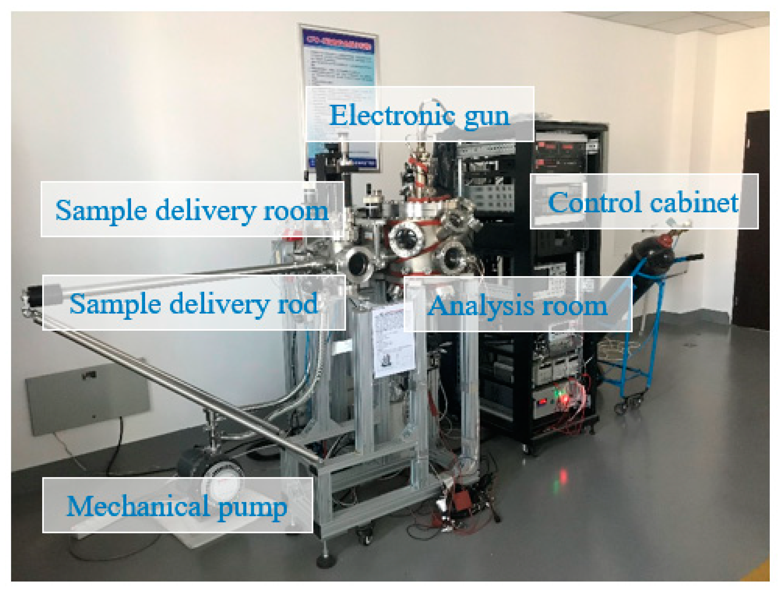
The experimental data were obtained from the Institute of Satellite Environmental Research in Beijing, China. The experimental equipment was a homemade secondary electron measurement device, as shown in Figure 1. The energy range of the electrons emitted by the electron gun was 50–5000 eV. The principle of the test is that the electrons emitted by the electron gun are incident on the surface of the material to be measured, and the secondary electrons and backscattered electrons excited by the incident electrons will escape from the surface of the material and then pass through the three-layer grids in turn and finally be collected by the collection pole. The total electrons and backscattered electrons are collected by adjusting the voltages of the three-layer grids. The backscattered electrons are collected when the grid voltage is −50 V. The total electrons are collected when the grid voltage is 0 V. The number of secondary electrons is calculated from the total electrons and backscattered electrons. Finally, the emission of the secondary electrons yield is calculated [44].

Figure 1.
Secondary electronic measuring device.
3. Results
3.1. Graphene and Polyimide SEY Simulation and Experimental Analysis
For individual graphene and polyimide materials, each material’s SEY was compared by simulation and experiment. As can be seen from Figure 2, the Monte Carlo simulation results were similar to the experimental results. This method can reproduce the maximum SEY position well and make accurate predictions and can also can prove the accuracy of the simulation. This good consistency enabled us to analyze the SEY effect of different graphene thicknesses on polyimide substrates and provided a basis for subsequent analysis.
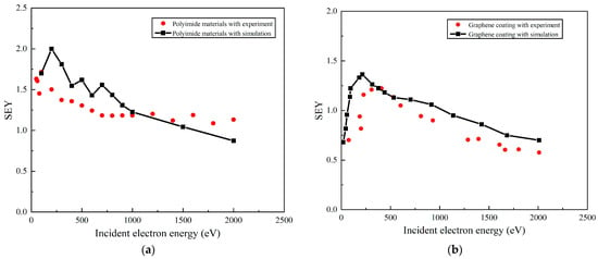
Figure 2.
Simulation and experimental comparison of SEY of polyimide and graphene, (a) is simulation and experimental comparison of SEY of polyimide and (b) is simulation and experimental comparison of SEY of graphene.
First of all, it can be seen from Figure 2 that the simulation method and the experimental measurement results have a good simulation effect within a certain range. The error may be due to the fact that polyimide is a polymer material, which will produce errors in the sample production. There will be tiny protrusions on its surface, but it is uniformly distributed in the simulation. Compared with the simulation, the error will be generated under the actual test conditions. The error is within an acceptable range, indicating that the numerical simulation method can better simulate the secondary electron emission phenomenon. The SEY of polyimide materials is an increasing function from 50 to 200 eV, while the SEY peak of graphene is smaller than that of polyimide materials in this energy range. It is consistent with the law in the literature and experiments [45,46,47]. The low SEY of graphene coating is the main reason that the graphene coating reduces the secondary electron emission of polyimide. The effects of different graphene thicknesses on the SEY will be analyzed in the next section.
3.2. Effects of Different Thickness Graphene Coatings on SEY
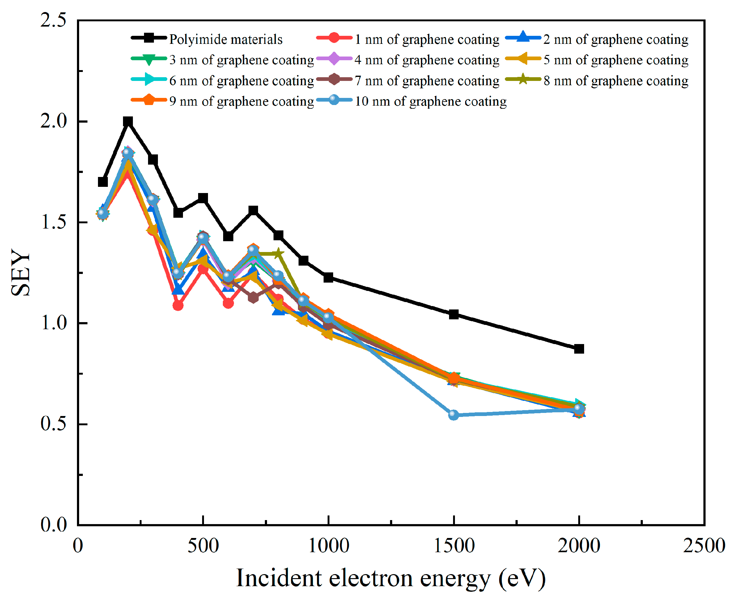
The effect of different graphene coating thickness on polyimide substrate on the SEY was simulated with GEANT4. As shown in Figure 3, it can be found that the graphene coating had a direct effect on the SEY and had a good suppression effect. From 1 to 10 nm of graphene coating, it can be seen that the SEY peak and shape of the sample materials were significantly changed, and the SEY curve was a combination of emission contributions from the polyimide and the graphene coating in this coating thickness range. It can be seen that the graphene coating has a good suppression effect on polyimide materials, and the suppression effect was best when the thickness of graphene coating was 1 nm and 5 nm. The maximum SEY was reduced by 13%. At a higher energy incidence, the coating at 5 nm shows a better effect. With the increase in thickness, the secondary electron emissivity decreases, but with a continuous increase, the secondary electron emissivity does not decrease, which is consistent with the law in the literature [48,49].
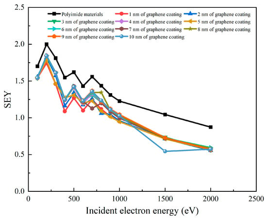
Figure 3.
Simulation of secondary electron yields of polyimide graphene coatings with different thicknesses.
At very low energies, the electron path length in carbon does not exceed a few nanometers. Thus, this behavior can be explained in terms of the penetration distance of the incident electron. The incident electron penetration depth is the average distance traveled by an incident electron projected in the direction of incidence in the irradiated material. The projected range of 300 eV incident electrons was about 1 nm in graphene, which was much smaller than the thickness of the covering layer. Not surprisingly, the secondary electron emission process was driven by the graphite coating. However, the actual range of the electrons was about 5 nm at 1 keV [50]. As the energy of the incident electrons increased, the electrons began to penetrate the polyimide substrate, and the effects of the polyimide began to be felt. Therefore, the very-low-energy electrons could only leave when they were produced to very close surfaces. This suggested that the graphene coating was a major contributor to the lowest-energy electron group. Most low-energy secondary electrons were produced on very close surfaces of irradiated materials. Depositing just a few nanometers of the graphene coating was enough to significantly alter the material’s SEY.
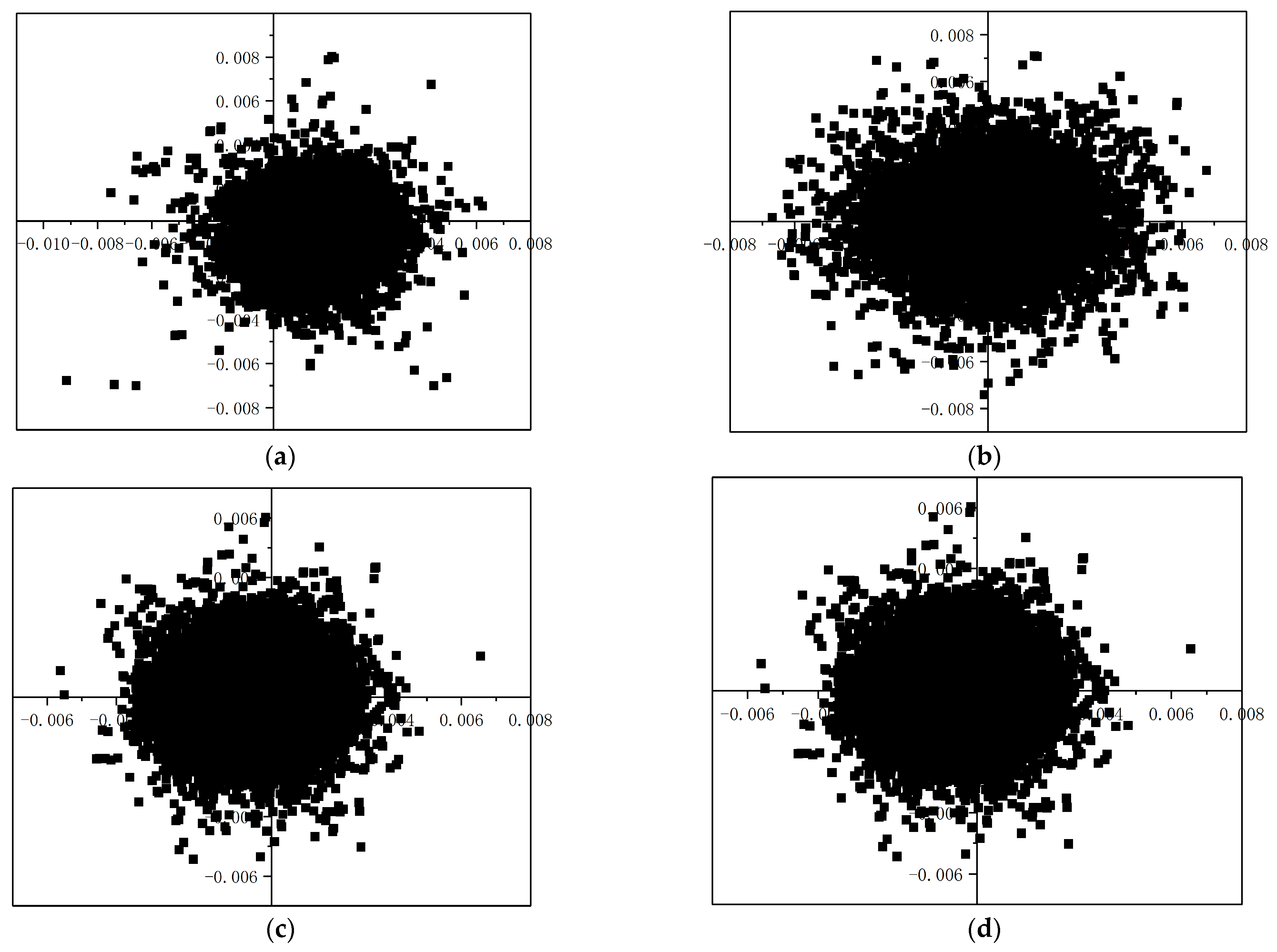
The 1, 3, 5, and 7 nm thicknesses of the graphene coating were selected to analyze the position of secondary electron emission. As shown in Figure 4, when the electron energy was 200 eV and the SEY reached the maximum, it can be clearly found that the secondary electron reaction range was larger when the graphene coating thickness was low. The secondary electron emission range decreased with the increase in the graphene coating thickness. This may be because the resistance and the binding of the secondary electrons in the material increased with the increase in the graphene coating. However, as the thickness of the graphene coating continued to increase, the secondary electron emission range approached constant. Therefore, the 5 nm thickness of the graphene coating can better reduce the secondary electron emission range.

Figure 4.
Location of secondary electron emission, (a) is 1 nm secondary electron emission location, (b) is 3 nm secondary electron emission location, (c) is 5 nm secondary electron emission location, and (d) is 7 nm secondary electron emission location.
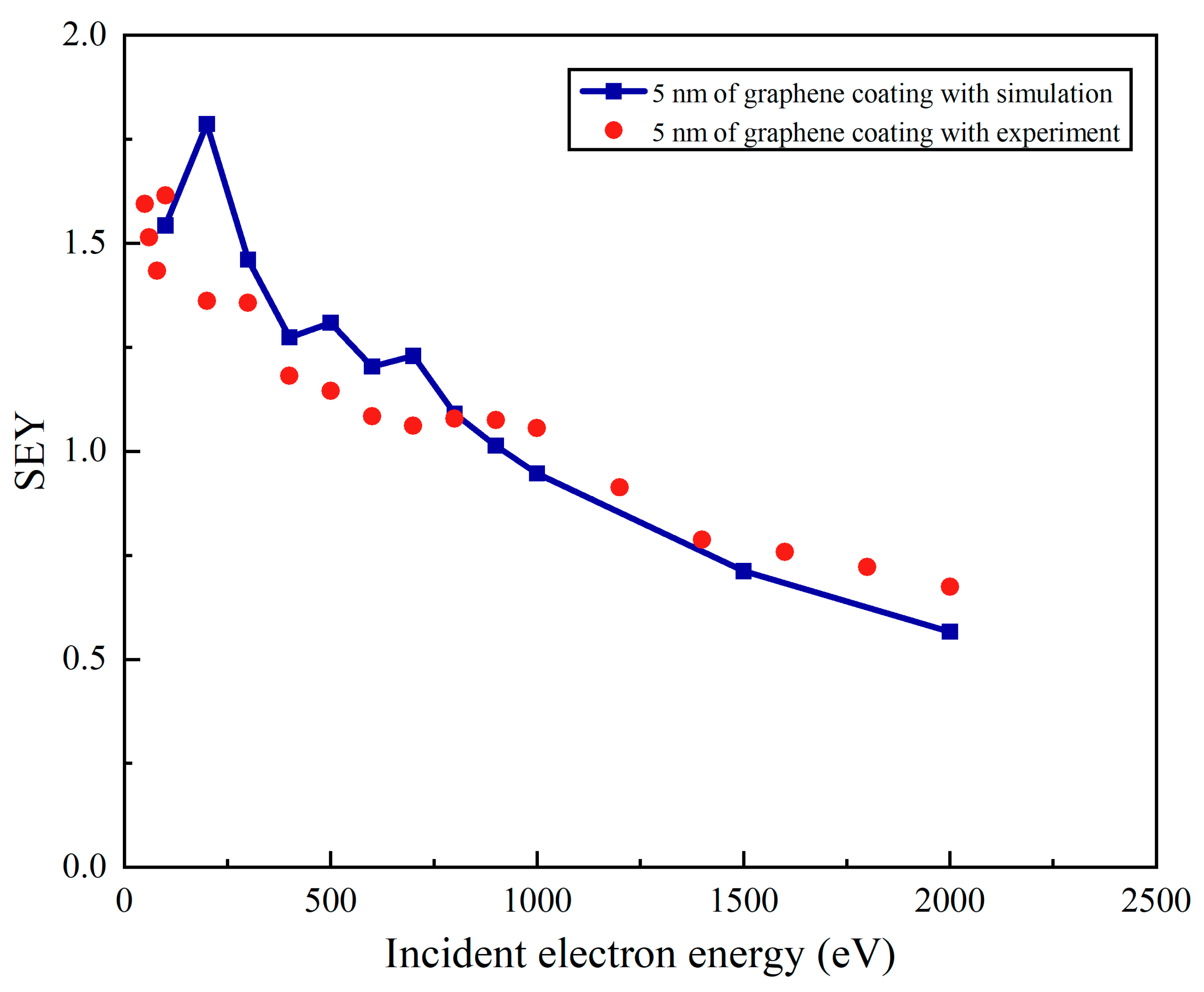
For the experimental verification of the 5 nm thickness, the CVD method was used to prepare five layers of graphene-coated polyimide material. The thickness of the graphene coating was about 5 nm. The verification results and simulation results are shown in Figure 5. The error may be due to the influence of thickness during the preparation process and environmental conditions during the experiment, and they have a good consistency within the allowed range of error. The 5 nm graphene coating reduced the secondary electron emission yield by 6% compared to the polyimide material from an experimental perspective. Therefore, the suppression of polyimide by the graphene coating was verified with the numerical simulation method, and it was concluded that 5 nm is one of the good thicknesses.

Figure 5.
Simulation and experimental SEY comparison of 5 nm of graphene coating.
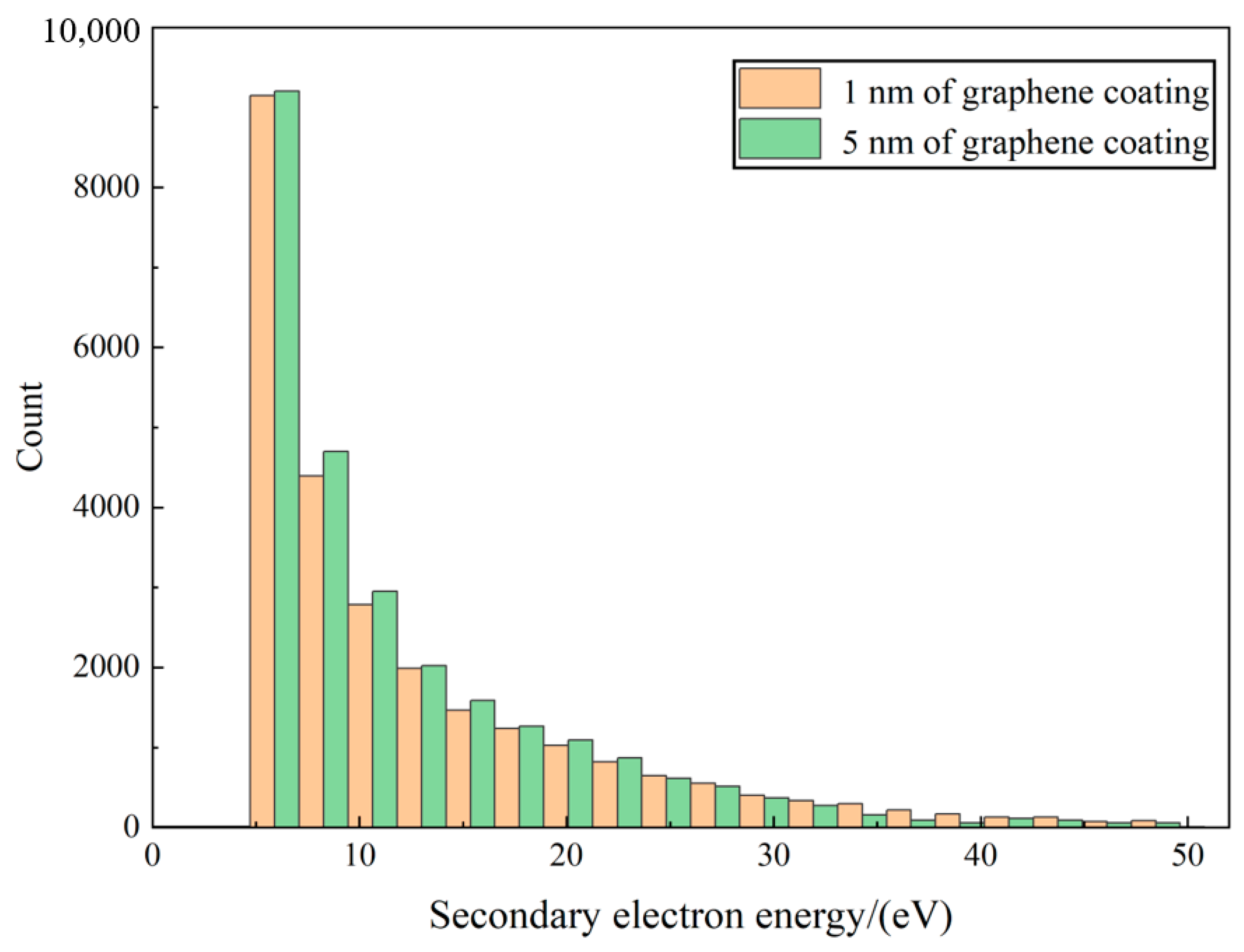
In order to analyze the influence of different thicknesses of graphene coating on the secondary electron emission energy, the 1 nm and 5 nm coatings with a better suppression effect on the secondary electron emission were selected for analysis. As shown in Figure 6, it can be found that the secondary electron emission energy was high when the thickness of the graphene coating was low. When the thickness of the graphene coating increased, the secondary electron emission energy decreased. This may be due to the higher energy consumption required to break through the higher surface barrier during the secondary electron emission as the thickness increased.
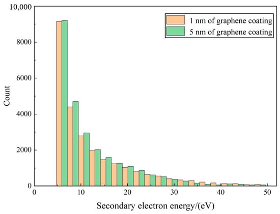
Figure 6.
Secondary electron emission energy of different thicknesses.
4. Conclusions
In this study, the secondary electron emission yields of polyimide and graphene materials were simulated using the GEANT4 numerical simulation method. For polyimide substrate materials, the secondary electron emission yields of graphene-coated materials with different thickness were studied using this method, and the suppression effect of graphene coatings with different thicknesses on the secondary electron emission was analyzed. The optimal graphene coating thicknesses of the lowest secondary electron yield of polyimide material were 1 nm and 5 nm, which can reduce the secondary electron emission yield by 13% from a simulation point of view. The 5 nm graphene coating reduced the secondary electron emission by 6% compared to the polyimide material from an experimental perspective. The 5 nm coating showed a better effect at a higher energy and was verified by the preparation of five layers of graphene coating. The results showed that the simulation was in good agreement with the experiment. At the same time, the displacement change of secondary electron emission on the surface was analyzed. With the increase in coating thickness, the emission displacement range decreased. The influence of different graphene thickness on the energy of secondary electron generation was studied. The research results can provide technical reference for the application of polyimide film materials in space and the simulation of secondary electron emission.
Author Contributions
X.Q.: conceptualization, methodology, formal analysis, and writing—original draft. Y.M.: conceptualization, methodology, project administration, and funding acquisition. S.L.: investigation and validation. T.Z.: resources and supervision. X.N.: resources and supervision. Y.W.: investigation and data curation. W.P.: resources and supervision. G.H.: conceptualization, supervision, and project administration. All authors have read and agreed to the published version of the manuscript.
Funding
This research was funded by the Aerospace Science and Technology Group Applied Innovation Program, grant number 6230114001, and Reliability and Environmental Engineering Technology Key Laboratory Fund Program, grant number 6142004210201.
Institutional Review Board Statement
Not applicable.
Informed Consent Statement
Not applicable.
Data Availability Statement
The data presented in this study are available on request from the corresponding author.
Conflicts of Interest
The authors declare no conflict of interest.
References
- Aguilera, L.; Montero, I.; Davila, M.E.; Ruiz, A.; Galan, L.; Nistor, V.; Raboso, D.; Palomares, J.; Soria, F. CuO nanowires for inhibiting secondary electron emission. J. Phys. D-Appl. Phys. 2013, 46, 165104. [Google Scholar] [CrossRef]
- Xie, A.; Guo, S.; Li, C.; Pei, Y. The measurement of secondary electron emission coefficient of MgO. J. Anhui University. Nat. Sci. 2006, 30, 61–64. [Google Scholar]
- Patino, M.; Raitses, Y.; Wirz, R. Secondary electron emission from plasma-generated nanostructured tungsten fuzz. Appl. Phys. 2016, 109, 201602. [Google Scholar] [CrossRef]
- Cao, W.; Wang, B.; Yang, Y.; Zhu, B.; Guo, J.; Xu, P.; Bai, X.; Qin, J.; Wang, C.; Zhu, J.; et al. Secondary electron emission characteristics of the Al2O3/MgO double-layer structure prepared by atomic layer deposition. Ceram. Int. 2021, 47, 9866–9872. [Google Scholar] [CrossRef]
- Cimino, R.; Commisso, M.; Grosso, D.; Demma, T.; Baglin, V.; Flammini, R.; Larciprete, R. Nature of the Decrease of the Secondary-Electron Yield by Electron Bombardment and its Energy Dependence. Phys. Rev. Lett. 2012, 109, 064801. [Google Scholar] [CrossRef] [PubMed]
- Cui, Y.; Song, B.; Yang, Y.; Huang, Y.; Zhou, R.; Cao, C.; Zhang, G.; Meng, N.; Zhao, S.; Ma, H. Study on Characteristics of Secondary Electron Emission for Spacecraft Surface Materials. Chin. J. Vac. Sci. Technol. 2021, 41, 770–774. [Google Scholar]
- Garcia-Valenzuela, A.; Muñoz-Piña, S.; Alcala, G.; Alvarez, R.; Lacroix, B.; Santos, A.; Cuevas-Maraver, J.; Rico, V.; Gago, R.; Vazquez, L.; et al. Growth of nanocolumnar thin films on patterned substrates at oblique angles. Plasma Process. Polym. 2019, 16, 1800135. [Google Scholar] [CrossRef]
- Li, Y.; Cui, W.-Z.; Wang, H.-G. Simulation investigation of multipactor in metal components for space application with an improved secondary emission model. Phys. Plasmas 2015, 22, 053108. [Google Scholar]
- Zhang, N.; Cao, M.; Cui, W.; Hu, T. Effect of rough surface morphology on secondary electron emission from metal surface. Jpn. J. Appl. Phys. 2017, 56, 075802. [Google Scholar] [CrossRef]
- Pivi, M.T.F.; Collet, G.; King, F.; Kirby, R.E.; Markiewicz, T.; Raubenheimer, T.O.; Seeman, J.; Le Pimpec, F. Experimental observations of in situ secondary electron yield reduction in the PEP-II particle accelerator beam line. Nucl. Inst. Methods Phys. Res. A 2010, 621, 47–56. [Google Scholar] [CrossRef][Green Version]
- Krasnov, A.A. Molecular pumping properties of the LHC arc beam pipe and effective secondary electron emission from Cu surface with artificial roughness. Vacuum 2004, 73, 195–199. [Google Scholar] [CrossRef][Green Version]
- Zhang, W.; Wang, Y.; Wang, S.; Fan, L.; Wei, W.; Fang, J.; Li, W.; Wang, Y. Study on the anisotropy of the secondary electron yield and resistance of the laser-etched copper. Appl. Surf. Sci. 2021, 564, 150419. [Google Scholar] [CrossRef]
- Valizadeh, R.; Malyshev, O.B.; Wang, S.; Zolotovskaya, S.; Gillespie, W.; Abdolvand, A. Low secondary electron yield engineered surface for electron cloud mitigation. Appl. Phys. Lett. 2014, 105, 231605. [Google Scholar] [CrossRef]
- Yamamoto, K.; Shibata, T.; Ogiwara, N.; Kinsho, M. Secondary electron emission yields from the J-PARC RCS vacuum components. Vacuum 2007, 81, 788–792. [Google Scholar] [CrossRef]
- Le Pimpec, F.; Kirby, R.; King, F.; Pivi, M. Properties of TiN and TiZrV thin film as a remedy against electron cloud. Nucl. Instrum. Methods Phys. Research. Sect. A Accel. Spectrometers Detect. Assoc. Equip. 2005, 551, 187–199. [Google Scholar] [CrossRef]
- Luo, J.; Tian, P.; Pan, C.; Robertson, A.; Warner, J.; Hill, E.; Briggs, G. Ultralow Secondary Electron Emission of Graphene. ACS Nano 2011, 5, 1047–1055. [Google Scholar] [CrossRef]
- Pisarra, M.; Riccardi, P.; Cupolillo, A.; Sindona, A.; Caputi, L. Studies of Electron Emission in the Interaction of Electrons with Graphene on Ni(111) Surface. Nanosci. Nanotechnol. Lett. 2012, 4, 1100–1103. [Google Scholar] [CrossRef]
- Zhang, Y.; Wang, Y.; Wang, S.; Wei, W.; Ge, X.; Zhu, B.; Shao, J.; Wang, Y. Comparison of Carbon Thin Films with Low Secondary Electron Yield Deposited in Neon and Argon. Coatings 2020, 10, 884. [Google Scholar] [CrossRef]
- Alvarado, A.; Chang, H.; Nadvornick, W.; Ghoniem, N.; Marian, J. Monte Carlo raytracing method for calculating secondary electron emission from micro-architected surfaces. Appl. Surf. Sci. 2019, 478, 142–149. [Google Scholar] [CrossRef]
- Chang, T.; Zheng, J. Monte-Carlo simulation of secondary electron emission from solid metal. Acta Phys. Sin. 2012, 61, 241401. [Google Scholar] [CrossRef]
- Polak, M.P.; Morgan, D. MAST-SEY: MAterial Simulation Toolkit for Secondary Electron Yield. A monte carlo approach to secondary electron emission based on complex dielectric functions. Comput. Mater. Sci. 2021, 193, 110281. [Google Scholar] [CrossRef]
- Yasuda, M.; Nobuo, T.; Kawata, H. A Monte Carlo calculation of secondary electron emission from organic compounds. Jpn. J. Appl. Phys. Part 1-Regul. Pap. Brief Commun. Rev. Pap. 2004, 43, 4004–4008. [Google Scholar] [CrossRef]
- Pierron, J.; Inguimbert, C.; Belhaj, M.; Gineste, T.; Puech, J.; Raine, M. Electron emission yield for low energy electrons: Monte Carlo simulation and experimental comparison for Al, Ag, and Si. J. Appl. Phys. 2017, 121, 215107. [Google Scholar] [CrossRef]
- Brieda, L.; Pai, S.; Keidar, M. Kinetic Analysis of Electron Transport in a Cylindrical Hall Thruster. IEEE Trans. Plasma Sci. 2011, 39, 2946–2947. [Google Scholar] [CrossRef]
- Hollmann, E.; Doerner, R.; Nishijima, D.; Pigarov, A. Observation of reduction of secondary electron emission from helium ion impact due to plasma-generated nanostructured tungsten fuzz. J. Phys. D-Appl. Phys. 2017, 50, 445203. [Google Scholar] [CrossRef]
- Li, Y.; Yan, Y.; Lin, S.; Wang, H.; Liu, C. A fast single particle Monte-Carlo method of computing the breakdown threshold of multipactor in microwave device. Acta Phys. Sin. 2014, 63, 78–84. [Google Scholar]
- Liu, L.; Liu, D.; Wang, X.; Peng, K.; Yang, C. Implementation of secondary emission in three dimensional PIC numerical simulation. High Power Laser Part. Beams 2012, 24, 1980–1984. [Google Scholar]
- Balcon, N.; Payan, D.; Belhaj, M.; Tondu, T.; Inguimbert, V. Secondary Electron Emission on Space Materials: Evaluation of the Total Secondary Electron Yield From Surface Potential Measurements. IEEE Trans. Plasma Sci. 2012, 40, 282–290. [Google Scholar] [CrossRef]
- Ashley, J.C.; Anderson, V.E. Interaction of low-energy electrons with silicon dioxide. J. Electron Spectrosc. Relat. Phenom. 1981, 24, 127–148. [Google Scholar] [CrossRef]
- Ashley, J.C. Interaction of low-energy electrons with condensed matter: Stopping powers and inelastic mean free paths from optical data. J. Electron Spectrosc. Relat. Phenom. 1988, 46, 199–214. [Google Scholar] [CrossRef]
- Ashley, J.C. Energy-loss probabilities for electrons, positrons, and protons in condensed matter. J. Appl. Phys. 1991, 69, 674–678. [Google Scholar] [CrossRef]
- Nguyen, H.; Mankowski, J.; Dickens, J.; Neuber, A.; Joshi, R. Calculations of secondary electron yield of graphene coated copper for vacuum electronic applications. Aip Adv. 2018, 8, 015325. [Google Scholar] [CrossRef]
- Pivi, M.; King, F.; Kirby, R.; Raubenheimer, T.; Stupakov, G.; Le Pimpec, F. Sharp reduction of the secondary electron emission yield from grooved surfaces. J. Appl. Phys. 2008, 104, 104904. [Google Scholar] [CrossRef]
- Ran, M.; Jia, L.; Cheng, C.; Wu, Q. Temperature-variable raman scattering study on micromechanical properties of the carbon fiber reinforced polyimide composite film. Carbon 2019, 150, 555. [Google Scholar] [CrossRef]
- Ruzic, D.; Moore, R.; Mans, D.; Cohen, S. Secondary-electron yields of carbon-coated and polished stainless-steel. J. Vac. Sci. Technol. 1982, 20, 1313–1316. [Google Scholar] [CrossRef]
- Allison, J.; Amako, K.; Apostolakis, J.; Arce, P.; Asai, M.; Aso, T.; Baglih, E.; Bagulyai, A.; Banerjee, S.; Barrand, G.; et al. Recent developments in Geant4. Nucl. Instrum. Methods Phys. Res. Sect. A 2016, 835, 186–225. [Google Scholar] [CrossRef]
- Röpke, G.; Selchow, A.; Wierling, A.; Reinholz, H. Lindhard dielectric function in the relaxation-time approximation and generalized linear response theory. Phys. Lett. A 1999, 260, 365–369. [Google Scholar] [CrossRef]
- Xie, A.; Pei, Y.; Wang, R.; Sun, H. Discussion of the improving secondary electron emission coefficient. High Power Laser Part. Beams 2005, 17, 279–282. [Google Scholar]
- Ye, M.; He, Y.; Hu, S.; Wang, R.; Hu, T.; Yang, J.; Cui, W. Suppression of secondary electron yield by micro-porous array structure. J. Appl. Phys. 2013, 113, 074904. [Google Scholar] [CrossRef]
- Llacer, J.; Garwin, E.L. Electron-Phonon Interaction in Alkali Halides. I. The Transport of Secondary Electrons with Energies between 0.25 and 7.5 eV. J. Appl. Phys. 1969, 40, 2766–2775. [Google Scholar] [CrossRef]
- Gibaru, Q.; Inguimbert, C.; Caron, P.; Raine, M.; Lambert, D.; Puech, J. Geant4 physics processes for microdosimetry and secondary electron emission simulation: Extension of MicroElec to very low energies and 11 materials (C, Al, Si, Ti, Ni, Cu, Ge, Ag, W, Kapton and SiO2). Nucl. Instrum. Methods Phys. Res. Sect. B-Beam Interact. Mater. At. 2021, 487, 66–77. [Google Scholar] [CrossRef]
- Sun, Y.; Xu, H.; Da, B.; Mao, S.; Ding, Z. Calculations of Energy-Loss Function for 26 Materials. Chin. J. Chem. Phys. 2016, 29, 663–667. [Google Scholar] [CrossRef]
- Da, B.; Shinotsuka, H.; Yoshikawa, H.; Ding, Z.; Tanuma, S. Extended Mermin Method for Calculating the Electron Inelastic Mean Free Path. Phys. Rev. Lett. 2014, 113, 063201. [Google Scholar] [CrossRef] [PubMed]
- Qi, X.; Ma, Y.; Liu, S.; Nie, X.; Zhang, T.; Wu, Y.; Peng, W.; Hu, G. Suppression of Secondary Electron Emissions on the Graphene-Coated Polyimide Materials Prepared by Chemical Vapor Deposition. Coatings 2023, 13, 1805. [Google Scholar] [CrossRef]
- Pinto, P.; Calatroni, S.; Neupert, H.; Letant-Delrieux, D.; Lucas, S. Carbon coatings with low secondary electron yield. Vacuum 2013, 98, 29–36. [Google Scholar] [CrossRef]
- Wang, J.; Wang, Y.; Xu, Y.; Zhang, Y.; Zhang, B.; Wei, W. Secondary electron emission characteristics of graphene films with copper substrate. Chin. Phys. C 2016, 40, 117003. [Google Scholar] [CrossRef]
- Zhang, N.; Cao, M.; Cui, W.; Hu, T.; Wang, R.; Li, Y. Analytical model of secondary electron yield from metal surface with regular structures. Acta Phys. Sin. 2015, 64, 207901. [Google Scholar] [CrossRef]
- Inguimbert, C.; Gibaru, Q.; Caron, P.; Angelucci, M.; Spallino, L.; Cimino, R. Modelling the impact on the secondary electron yield of carbon layers of various thicknesses on copper substrate. Nucl. Instrum. Methods Phys. Res. Sect. B-Beam Interact. Mater. At. 2022, 526, 1–8. [Google Scholar] [CrossRef]
- Zhang, H.; Ge, Y.; Pan, P.; Du, Y.; Fu, H.; Yan, M.; Li, P.; Long, H.; Zhang, C.; Cai, J.; et al. Suppression of secondary electron emission on oxygen-free copper surface of reduced graphene oxide coatings prepared by electrophoretic deposition. Appl. Surf. Sci. 2022, 603, 154490. [Google Scholar] [CrossRef]
- Gibaru, Q.; Inguimbert, C.; Caron, P.; Belhaj, M.; Raine, M.; Lambert, D. Surface ionizing dose deposited by low energy electrons (10 eV–10 keV) in eleven monoatomic materials: Monte Carlo calculations and analytical expressions. Appl. Surf. Sci. 2022, 576, 151813. [Google Scholar] [CrossRef]
Disclaimer/Publisher’s Note: The statements, opinions and data contained in all publications are solely those of the individual author(s) and contributor(s) and not of MDPI and/or the editor(s). MDPI and/or the editor(s) disclaim responsibility for any injury to people or property resulting from any ideas, methods, instructions or products referred to in the content. |
© 2023 by the authors. Licensee MDPI, Basel, Switzerland. This article is an open access article distributed under the terms and conditions of the Creative Commons Attribution (CC BY) license (https://creativecommons.org/licenses/by/4.0/).

