Article

Effect of Low-Energy Implantation of In+ Ions on the Composition and Electronic Structure of Single-Crystal GaP(111)

by
Sardor Donaev
1,2,*,
Ganjimurod Shirinov
1,
Baltokhodja Umirzakov
1,3,
Burkhan Donayev
4 and
Shenghao Wang
5,*
1
Department of Electronic Equipment Production Technology, Faculty of Electronics and Automation, Tashkent State Technical University Named after Islam Karimov, Tashkent 100095, Uzbekistan
2
Department of Theoretical and Experimental Physics, Faculty of Physics, Karshi State University, Karshi 180119, Uzbekistan
3
Institute of Ion-Plasma and Laser Technologies, Uzbekistan Academy of Sciences, Tashkent 100125, Uzbekistan
4
Karshi Engineering-Economical Institute, Karshi 180100, Uzbekistan
5
Materials Genome Institute, Shanghai University, Shanghai 200444, China
*
Authors to whom correspondence should be addressed.
Coatings 2024, 14(10), 1231; https://doi.org/10.3390/coatings14101231
Submission received: 14 March 2024 / Revised: 11 September 2024 / Accepted: 18 September 2024 / Published: 24 September 2024

Abstract

:
Using a complex of secondary and photoelectron spectroscopy methods, the effects of the implantation of In+ ions with an energy of E0 = 1 keV at different doses and subsequent annealing on the composition, electronic, and crystal structure of the GaP(111) surface were studied. It is shown that in the dose range D ≈ 5 × 10¹⁴–5 × 1015 cm−2 after annealing, nanocrystalline phases Ga0.6In0.4P are formed with surface dimensions d ≈ 10–30 nm, and at D ≥ 6 × 1016 cm−2 nanofilm–Ga0.6In0.4P with a thickness of 30–35 nm. It has been found that the band gap of nanophases (Eg ≈ 2–2.3 eV) is much larger than Eg of the film (~1.85 eV). For the first time, information was obtained on the density of state of electrons in the valence band of nanophases and nanofilm GaInP.

1. Introduction

Interest in nanosized structures grown on the basis of GaP is due to their wide use and their promise in the creation of a monolithic optoelectronic integrated circuit (MOEIC), photoelectric generators (solar cells), optical and electronic pumping lasers, and microwave technology devices [1,2,3,4,5,6]. Therefore, electronic, optical, emission, and electrophysical properties and the influence of various effects on these properties are currently being intensively studied. In particular, to create an MOEIC on a Si substrate, it will be necessary to grow an epitaxial film with a direct gap transition on its surface [1,7]. GaP lattice constants and Si practically coincide with each other, so it is possible to obtain a heteroepitaxial GaP/Si system.
Methods of molecular beam epitaxy [1,2,3,4,5,6,7,8,9], liquid phase and vapor phase epitaxy [10,11,12,13,14,15,16], MOCVD [5,17,18,19], and high-energy ion implantation [20,21,22] are widely used to obtain three- and four-component layers on the GaP surface. In recent years, low-energy ion implantation is often used to obtain nanosized structures on the surface and in the near-surface region of materials [23,24,25,26,27,28,29,30,31,32].
In [20], GaAlA nanophases and nanofilms were obtained by implanting Al ions into GaP(111) and GaAs(111). It has been established that in the case of GaAlP nanophases with surface sizes less than 35–40 nm and a thickness of 3.5–4 nm, quantum size effects appear. However, to date, nanoscale structures of the GaInP type have not been obtained by low-energy ion implantation.
The results of such studies are very important for elucidating the basic mechanisms of the formation of nanofilm heteroepitaxial systems based on A3B5 binary semiconductors, as well as for the development of new opto- and nanoelectronic devices.
In this work, the composition, electronic, and crystal structure of GaInP nanostructures obtained by implanting In+ ions into GaP(111) with E0 = 1 keV with different doses of D were studied for the first time. For comparison, the surface morphology of the GaInP/GaP(111) MBE film was also studied.

2. Experimental Method

Standard single-crystal samples of n-type GaP(111) (n = 3∙1017 cm−3) grown by the Czochralski method with a diameter of ~10 mm and a thickness of 1 mm were chosen as objects of study (samples were obtained from the Institute of Crystallography, Russia). Before ion implantation, GaP(111) was degassed under ultra-high vacuum conditions (P = 10−7 Pa) at T = 900 K for ~4 h. An ultra-high vacuum in the device was created by an oil-free pumping system: two zeolite sorption pumps and a cooled titanium getter pump. The experimental device consists of two chambers. In the first chamber, all technological operations (thermal heating, ion implantation) were carried out, and in the second chamber, the composition and electronic structure of the materials under research were studied using the methods of Auger electron spectroscopy (AES) (A.F.Ioffe Physical-Technical Institute, Russia) and ultraviolet photoelectron spectroscopy (UVES) (UV-1280, Shimadzu, Japan). The spectra of Auger electrons and photoelectrons were recorded using a four-grid electron analyzer. To determine the depth distribution profile of the atoms, a layer-by-layer Auger analysis was carried out by sputtering the sample surface with Ar+ ions with an energy of 1 keV at an incidence angle of ∼80–85° relative to the normal; the etching rate was ∼(5 ± 1) Å/min. Ultraviolet photoelectron spectra were recorded at photon energy hν ≈ 10.8 eV. The photon source was a standard gas-discharge hydrogen lamp. Studies of the morphology of the crystalline structure of the surface of the samples were carried out in standard installations of scanning electron microscopy (SEM) (JSM-7200F), atomic force microscopy AFM (XE-100), and high-energy electron diffraction RHEED (EMR-2). The width of the forbidden zone was determined by a UV-1280 spectrophotometer.

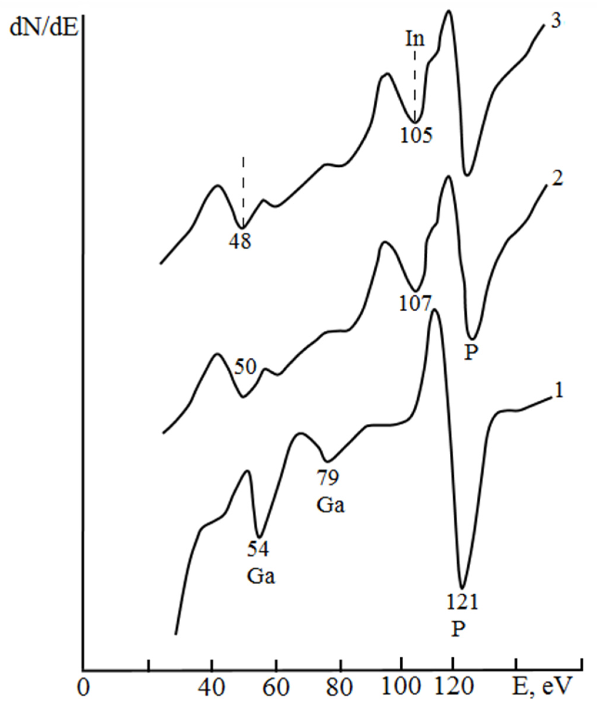
3. Experimental Results
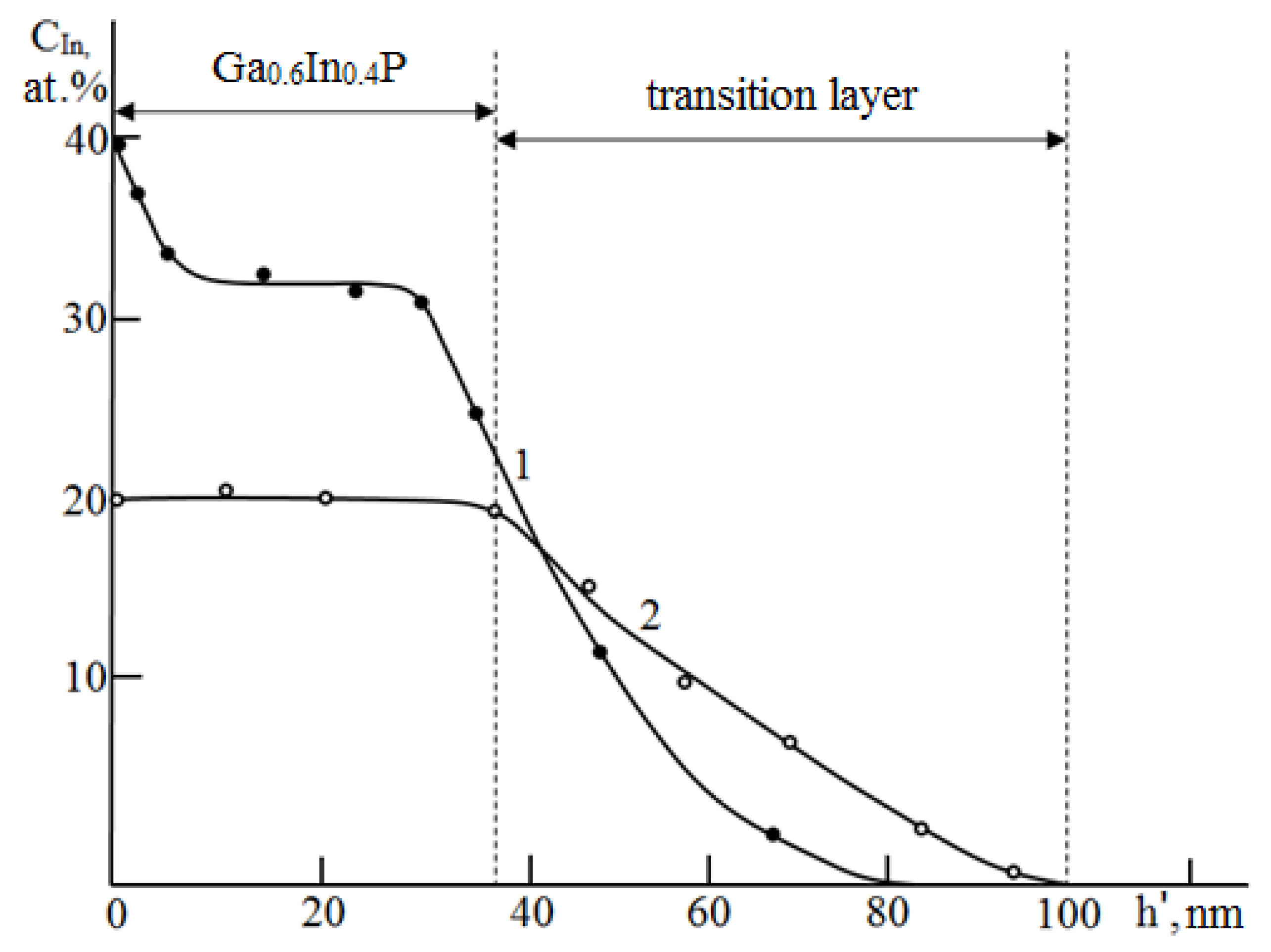
Figure 1 shows the initial part of the Auger spectra of pure GaP(111) and GaP implanted with In+ ions with an energy of 1 keV at D = Dsat ≈ 6∙1016 cm−2 before and after heating at a temperature T = 950 K (where Dsat—In ion saturation dose). Warm-up time ~30 min. It can be seen that after implantation of In+ ions, the intensity of the Ga and P Auger peaks in the spectrum decreases significantly and intense peaks characteristic of In appear. Ion-implanted layers are highly disordered up to amorphization. Calculations based on the full spectrum of Auger electrons of an ion-implanted sample using the formula [25] C x = I x / S x I i / S i showed that the surface concentrations of In, Ga, and P are, respectively, 40–45 at.%, 30–35 at.%, and 25–30 at.%. After heating this system at T = 950 K, the surface concentration of these atoms changes sharply: CGa ≈ 28–33 at.%, CIn ≈ 20–22 at.%, CP ≈ 48–52 at.%, i.e., a single-crystal film with an approximate composition of Ga0.6In0.4P with a thickness of ~30–35 Å was formed.
Figure 2 shows the concentration profiles of the distribution of In atoms over the depth h′ for GaP(111) implanted with In+ ions with E0 = 1 keV at D = 6 × 1016 cm−2, obtained before and after heating. It can be seen that after ion implantation, the surface concentration of In atoms is ~40–45 at.%. With an increase in h′ to ~8–10 Å, the CIn value sharply decreases by ~8–10 at.%. In the range h ≈ 10–25 nm, the In concentration does not change noticeably, and in the range h′ ≈ 25–80 Å, it decreases to a bullet. After heating at T = 950 K, the value of CIn on the surface decreases to 20–22 at.%, and it practically does not change until a depth of 35–40 Å. In the range h′ ≈ 40–100 Å, CIn monotonically decreases to 0, i.e., after heating, the concentration of atoms in the transition layer increases slightly.
Figure 1. Auger spectra: 1—pure GaP(111); 2—GaP(111), implanted with In+ ions with E0 = 1 keV at D = 6 × 1016 cm−2; 3—after annealing at T = 950 K. Annealing time 40 min.
Coatings 14 01231 g001
A comparison of the areas under the CIn(h′) curves shows that after heating it noticeably decreases. Apparently, during the heating process, along with some diffusion of In atoms into the depths of GaP, their evaporation from the surface layers occurs.
Figure 2. Profiles of the distribution of In atoms over the depth h′ for GaP(111) implanted with In+ ions with E0 = 1 keV at D = 6 × 1016 cm−2 before (curve 1) and after heating at T = 950 K (curve 2).
Coatings 14 01231 g002
Figure 3 shows SEM and AFM images of the surface of pure GaP(111) and GaP(111) with Ga0.6In0.4P surface films, obtained by MBE (h = 50 nm) and ion implantation (h = 0.35–0.4 nm) methods. From Figure 3, it is clear that the surface of single-crystal GaP(111) is atomically smooth. The estimated value of surface roughness, which was determined by AFM, is ~1 nm. Analysis of picture 3b shows that the MBE of the Ga0.6In0.4P film consists of individual blocks. In this case, the surface roughness increases to 5–6 nm (Figure 3d). The surface of Ga0.6In0.4P obtained by ion implantation in combination with heating is highly smooth, and the roughness is ~2 nm (Figure 3e).
Figure 4 shows HSED images of the surface of a pure GaP and GaP sample with a Ga0.6In0.4P film with a thickness of 3–3.5 nm. The images clearly reveal reflections characteristic of cubic lattices. However, in the case of a three-component film, the reflections are bolder and blurrier. This is apparently due to some discrepancy between the lattice parameters of GaP and GaInP (see Table 1).
Figure 5 shows the photoelectron spectra obtained after heating at T = 950 K (heating time 40 min) of GaP implanted with In+ ions with E0 = 1 keV at doses of 1015 (curve 2) and 6 × 1016 cm−2 (curve 3) [29,32]. In the first case, nanocrystalline phases with surface diameters d = 15–20 nm were formed, and in the second case, a Ga0.6In0.4P film was formed. These spectra well reflect the distribution of the density of the state of the valence band electrons. It can be seen that the spectrum of pure GaP exhibits maxima at binding energies of Ecb ≈–0.8 eV; –2.2 eV; and 4 eV, probably due to the excitation of electrons from the 4p and 4p + 4s states of Ga, as well as the hybridization of the 4s states of Ga with the 3s states of P (Figure 5, curve 1) [29,32]. In the case of the Ga0.6In0.4P film, the spectrum (Figure 5, curve 3) contains intense peaks with Ecb = −1.2; −3.3; and −5.6 eV, apparently associated with the excitation of electrons from the hybridized states of electrons 4s(Ga) + 5p(In), 4s(Ga) + 5p(In) + 3d(P), and 4s (Ga) + 5s(In) + 3d(P). The spectrum of GaP with Ga0.6In0.4P nanocrystals reveals some features characteristic of both GaP and Ga0.6In0.4P (Figure 5, curve 2).
To estimate the band gap of these samples, light absorption spectra were recorded (Figure 6), where K is the light absorption coefficient. It is known that at medium doses (5 × 10¹⁴–5∙1015 cm−2), the ion-implanted surface consists of two phases: the ion-doped phase and the undoped portions of the semiconductor [29]. In our case, at D = 1015 cm−2, the average surface diameters of the nanophases were d ~ 15–20 nm, and at D = 6 × 1016 cm−2 they were 25-30 nm. The distance between the centers of the phases is ~50–60 nm. In the case of D ≈ 6 × 1016 cm−2, after heating, a continuous homogeneous layer (film) of Ga0.6In0.4P with h = 35–40 Å is formed. Figure 6 shows that in all dependences K(hν), first with increasing hν, the value of K practically does not change, and then K sharply decreases, where
K = I0/In
I0 is the intensity of light passing through GaP, and In is the intensity of light passing through GaP with a GaInP nanostructure.
Figure 6. Spectra of light transmission through GaP(111) (curve 1) and GaP(111) with nanophases with surface diameters d ≈ 15–20 nm (2), d = 25–30 nm (3), and Ga0.6In0.4P nanofilm (4).
Coatings 14 01231 g006
In the case of GaP and GaP with a Ga0.6In0.4P film, a decrease in K is observed starting from hν ≈ 2.2 eV (curve 1) and hν ≈ 1.7 eV (curve 4), respectively, and in the case of GaP with Ga0.6In0.4P nanocrystals, a sharp decrease in K is observed in two values of hν [33]. The first decrease is associated with light absorption in areas coated with GaInP nanocrystals, and the second-in areas of GaP are not coated with nanocrystals. The extrapolation of a sharply decreasing part of the curves to the hν axis gives a value of Eg for a given material. It can be seen that Eg for GaP(111) is approximately equal to 2.36 eV, for a Ga0.6In0.4P film ~1.85 eV, and for nanocrystalline Ga0.6In0.4P phases with d = 25 nm ~2.3 eV and d = 25–30 nm ~2.3 eV. With increasing surface diameters d nanotimes, the K(hν) curves shift towards lower energies, i.e., Eg decreases (Table 1). Based on curve 2 (Figure 6), one can estimate the degree of coverage of the GaP(111) surface with GaInP Ѳ nanophases using the following formula [33]:
Ѳ = 1 − K.
In the case of GaP with GaInP nanocrystals, the value of Ѳ ≈ 0.40. Table 1 shows the values of Eg and Ѳ for the samples under study.
Table 1. Dimensions of nanostructures (thickness h and surface diameter d) and values of Eg and Ѳ of nanophases and GaInP films.
Studied Samplesh, nmd, nmEg, eVѲ, %
GaP(111)Monocrystal sample2.360
Ga0.6In0.4P/GaP(111)3–3.515–202.340
3–3.525–302.070
3–3.5continuous film1.85100
From Figure 5 and the table, it can be seen that, at the same thicknesses, the values of Eg for nanocrystalline phases are greater than for the film. These results show that in nanocrystalline phases, starting from a diameter of ≈ 25–30 nm, the value of Eg increases with decreasing d.

4. Conclusions

For the first time, nanocrystalline phases and Ga0.6In0.4P films with a thickness of 30–35 Å were obtained by the implantation of In+ ions in combination with annealing on the GaP(111) surface. Their parameters of energy bands and density of valence band electrons, as well as the degree of coverage of the GaP surface with Ga0.6In0.4P nanophases, were determined. It has been shown that in GaInP nanocrystals, the Eg value is greater than the Eg of the nanofilm.

Author Contributions

Conceptualization, B.U.; Validation, B.U.; Formal analysis, S.W.; Investigation, S.D., G.S., B.U., B.D. and S.W.; Resources, G.S.; Writing—original draft, B.U.; Writing—review & editing, G.S. and B.U.; Supervision, S.D., B.U. and S.W.; Project administration, S.D. All authors have read and agreed to the published version of the manuscript.

Funding

This research received no external funding.

Institutional Review Board Statement

Not applicable.

Informed Consent Statement

Not applicable.

Data Availability Statement

The data that support the findings of this study are available from the corresponding author on reasonable request.

Conflicts of Interest

The authors declare no competing interests.

References

  1. Lazarenko, A.A.; Nikitina, E.V.; Pirogov, E.V.; Sobolev, M.S.; Egorov, A.Y. Molecular beam epitaxy of GaPN, GaPAsN, and InGaPN nitride solid solutions. Semiconductors 2014, 48, 392–396. [Google Scholar] [CrossRef]
  2. Abramkin, D.S.; Petrushkov, M.O.; Emelyanov, E.A.; Nenashev, A.V.; Yesin, M.Y.; Vasev, A.V.; Putyato, M.A.; Bogomolov, D.B.; Gutakovskiy, A.K.; Preobrazhenskiy, V.V. Formation of InAs/GaP Quantum-Well Heterostructures on Silicon Substrates by Molecular-Beam Epitaxy. Semiconductors 2021, 55, 139–146. [Google Scholar] [CrossRef]
  3. Sun, C.; Wade, M.T.; Lee, Y.; Orcutt, J.S.; Alloatti, L.; Georgas, M.S.; Waterman, A.S.; Shainline, J.M.; Avizienis, R.R.; Lin, S.; et al. Single-chip microprocessor that communicates directly using light. Nature 2015, 528, 534–538. [Google Scholar] [CrossRef] [PubMed]
  4. Uvarova, A.V.; Baranova, A.I.; Vyacheslavovaa, E.A.; Kalyuzhnyic, N.A.; Kudryashova, D.A.; Maksimovaa, A.A.; Morozova, I.A.; Mintairovc, S.A.; Saliic, R.A.; Gudovskikha, A.S. Formation of Heterostructures of GaP/Si Photoconverters by the Combined Method of MOVPE and PEALD. Tech. Phys. Lett. 2021, 47, 730–733. [Google Scholar] [CrossRef]
  5. Ladugin, M.A.; Andreev, A.Y.; Yarotskaya, I.V.; Ryaboshtan, Y.L.; Bagaev, T.A.; Padalitsa, A.A.; Marmalyuk, A.A.; Vasilev, M.G. Comparative Study of GaAs/GaInP and GaAs/AlGaAs Quantum Wells Grown by Metalorganic Vapor Phase Epitaxy. Inorg. Mater. 2019, 55, 315–319. [Google Scholar] [CrossRef]
  6. Razeghi, M. Technology of Quantum Devices; Springer: Boston, MA, USA, 2010; 560p. [Google Scholar]
  7. Gudovskikh, A.S.; Uvarov, A.V.; Morozov, I.A.; Bukatin, A.S.; Baranov, A.I.; Kudryashov, D.A.; Kalyuzhnyy, N.A.; Mintairov, S.A.; Zubkov, V.I. Study of GaP Nucleation Layers Grown on Si by Plasma-Enhanced Atomic Layer Deposition. Phys. Status Solidi A 2019, 217, 1900532. [Google Scholar] [CrossRef]
  8. Kunert, B.; Reinhard, S.; Koch, J.; Lampalzer, M.; Volz, K.; Stolz, W. First demonstration of electrical injection lasing in the novel dilute nitride Ga (NAsP)/GaP-material system. Phys. Status Solidi C 2006, 3, 614. [Google Scholar] [CrossRef]
  9. Sobolev, M.S.; Lazarenko, A.A.; Nikitina, E.V.; Pirogov, E.V.; Gudovskikh, A.S.; Egorov, A.Y. MBE Growth of GaP on a Si Substrate. Semiconductors 2015, 49, 559–562. [Google Scholar] [CrossRef]
  10. Gudovskikh, A.S.; Kalyuzhnyy, N.A.; Lantratov, V.M.; Mintairov, S.A.; Shvarts, M.Z.; Andreev, V.M. Properties of interfaces in GaInP solar cells. Semiconductors 2009, 43, 1363–1368. [Google Scholar] [CrossRef]
  11. Baranov, A.I.; Uvarov, A.V.; Maksimova, A.A.; Vyacheslavova, E.A.; Kalyuzhnyy, N.A.; Mintairov, S.A.; Salii, R.A.; Yakovlev, G.E.; Zubkov, V.I.; Gudovskikh, A.S. Study of InP/GaP quantum wells grown by vapor phase epitaxy. Tech. Phys. Lett. 2023, 49, 163–167. [Google Scholar]
  12. Dvoretckaia, L.N.; Bolshakov, A.D.; Mozharov, A.M.; Sobolev, M.S.; Kirilenko, D.A.; Baranov, A.I.; Mikhailovskii, V.Y.; Neplokh, V.V.; Morozov, I.A.; Fedorov, V.V.; et al. GaNP-based photovoltaic device integrated on Si substrate. Sol. Energy Mater. Sol. Cells 2019, 206, 110282. [Google Scholar] [CrossRef]
  13. Baranov, A.I.; Gudovskikh, A.S.; Egorov, A.Y.; LeGall, S.; Kudryashov, D.A.; Kleider, J.P. Defect properties of solar cells with layers of GaP based dilute nitrides grown by molecular beam epitaxy. J. Appl. Phys. 2020, 128, 023105. [Google Scholar] [CrossRef]
  14. Chang, L.L.; Ploog, K. (Eds.) Molecular Beam Epitaxy and Heterostructures; Springer: Dordrecht, The Netherlands, 2012; 728p. [Google Scholar]
  15. Fedorchenko, I.V.; Kushkov, A.R.; Gaev, D.S.; Rabinovich, O.I.; Marenkin, S.F.; Didenko, S.I.; Legotin, S.A.; Orlova, M.N.; Krasnov, A.A. Growth method for AIIIBV and AIVBVI heterostructures. J. Cryst. Growth 2018, 483, 245–250. [Google Scholar] [CrossRef]
  16. Mori, M.J. Lattice Mismatched Epitaxy of Heterostructures for Non-Nitride Green Light Emitting Devices. Ph.D. Thesis, Massachusetts Institute of Technology, Cambridge, MA, USA, June, 2008. [Google Scholar]
  17. Uvarova, A.V.; Sharova, V.A.; Kudryashova, D.A.; Gudovskikha, A.S. Impact of Silicon Wafer Surface Treatment on the Morphology of GaP Layers Produced by Plasma Enhanced Atomic Layer Deposition. Semiconductors 2023, 57, 415–422. [Google Scholar] [CrossRef]
  18. Uvarov, A.V.; Gudovskikh, A.S.; Nevedomskiy, V.N.; Baranov, A.I.; Kudryashov, D.A.; Morozov, I.A. Low temperature epitaxial growth of GaP on Si by atomic-layer deposition with plasma activation. J. Phys. D Appl. Phys. 2020, 53, 345105. [Google Scholar] [CrossRef]
  19. Zhang, X.B.; Ryou, J.H.; Dupius, R.D.; Walter, G.; Holonyak, N. Metalorganic Chemical Vapor Deposition Growth and Characterization of GaInP/GaAs Superlattices. J. Electron. Mater. 2006, 35, 705–710. [Google Scholar] [CrossRef]
  20. Ushakov, V.V.; Dravin, V.A.; Melnik, N.N.; Zavaritskaya, T.V.; Loiko, N.N.; Karavanskii, V.A.; Timoshenko, V.Y. Ion implantation of porous gallium phosphide. Semiconductors 1998, 32, 886–890. [Google Scholar] [CrossRef]
  21. Bhattachar-Yaa, D.; Vinokurov, D.A.; Gusinskii, G.M.; Elyukhin, V.A.; Kovalenkov, O.V.; Kyutt, R.N.; Marsh, J.H.; Naidenov, V.O.; Portnoi, E.L. Low-temperature photoluminescence of heavy-ion-implanted InGaP solid solutions. Tech. Phys. Lett. 1998, 24, 690–691. [Google Scholar] [CrossRef]
  22. Evtushenko, N.G.; Stukalov, S.A. Defect formation in GaP during laser implantation of impurities of groups I and III. Bull. Odesnik State Univ. 2000, 5, 196–201. [Google Scholar]
  23. Donaev, S.B.; Djurabekova, F.; Tashmukhamedova, D.A.; Umirzakov, B.E. Formation of nanodimensional structures on surfaces of GaAs and Si by means of ion implantation. Phys. Status Solidi C 2015, 12, 89–93. [Google Scholar] [CrossRef]
  24. Ergashov, Y.S.; Tashmukhamedova, D.A.; Umirzakov, B.E. On the Synthesis of Nanoscale Phases of Metal Silicides in the Near-Surface Region of Silicon and the Study of Their Electronic Structures by Passing Light. J. Surf. Investig. X-ray Synchrotron Neutron Tech. 2017, 11, 480–484. [Google Scholar] [CrossRef]
  25. Donaev, S.B.; Umirzakov, B.E. Effect of the Implantation of Al+ Ions on the Composition, Electronic and Crystalline Structure of the GaP(111) Surface. Semiconductors 2020, 54, 860–862. [Google Scholar] [CrossRef]
  26. Karimov, M.K.; Kutliev, U.O.; Bobojonova, S.B.; Otabaeva, K.U. Investigation of Angular Spectrum of Scattered Inert Gas Ions from the InGaP (001) Surface. Phys. Chem. Solid State 2021, 22, 742–745. [Google Scholar] [CrossRef]
  27. Kutliev, U.; Karimov, M.; Sadullaeva, B.; Otaboev, M. Investigation of the ion scattering process from the A3B5 semiconductors by the computer simulation method. Compusoft 2018, 7, 2749–2751. [Google Scholar]
  28. Chanda, A.; Lenka, H.P.; Jacob, C. Study of high energy Mn+1 ion implantation in GaAs. Appl. Phys. A 2009, 94, 89–94. [Google Scholar] [CrossRef]
  29. Shirinov, G.M.; Donaev, S.B.; Umirzakov, B.Y.; Loboda, V.V. Emission, optical and electrical properties of GaInP/GaP nanofilms. St. Petersburg State Polytech. Univ. J. Phys. Math. 2023, 16, 89–97. [Google Scholar]
  30. Normurodov, M.T.; Rysbaev, A.S.; Bekpulatov, I.R.; Normurodov, D.A.; Tursunmetova, Z.A. Formation and electronic structure of barium-monosilicide and barium-disilicide films. J. Surf. Investig. 2021, 15, S211–S215. [Google Scholar] [CrossRef]
  31. Rysbaev, A.S.; Khuzhaniyazov, Z.B.; Normuradov, M.T.; Rakhimov, A.M.; Bekpulatov, I.R. Peculiarities of the electron structure of nanosized ion-implanted layers in silicon. Tech. Phys. 2014, 59, 1705–1710. [Google Scholar] [CrossRef]
  32. Donaev, S.B.; Karimova, V.N.; Azimov, A.T.; Boltaboyev, K.; Yakubova, M.M. Using of ion implantation for obtaining nanostructures with the wide band GaP based on GaP. IOP Conf. Ser. Earth Environ. Sci. 2020, 614, 012002. [Google Scholar] [CrossRef]
  33. Altukhov, A.A.; Zhirnov, V.V. Analysis of the morphology and stocsiometry of CoSi2/Si(100) films obtained by SPE and RE methods. In Proceedings of the II All-Union Conference, Moscow, Izhevsk, Russia, 23–25 October 1991; pp. 15–22. [Google Scholar]
Figure 3. SEM (ac) and AFM (d,e) images of the GaP surface with Ga0.6In0.4P surface films obtained by MBE with d ≈ 50 nm (b,d) and ion implantation in combination with heating with d ≈ 3.5–4 nm (c,e).
Coatings 14 01231 g003
Figure 4. HSED images of the surface of GaP (a) and GaP with a Ga0.6In0.4P film (b).
Coatings 14 01231 g004
Figure 5. Photoelectron spectra obtained after heating at T = 950 K of GaP(111) implanted with In+ ions with E0 = 1 keV at doses D, cm−2: 1—0; 2—1015; 3—6 × 10¹⁶. Annealing time t ≈ 40 min [29,32].
Coatings 14 01231 g005
Disclaimer/Publisher’s Note: The statements, opinions and data contained in all publications are solely those of the individual author(s) and contributor(s) and not of MDPI and/or the editor(s). MDPI and/or the editor(s) disclaim responsibility for any injury to people or property resulting from any ideas, methods, instructions or products referred to in the content.

