Article

Extracting the Optical Constants of Partially Absorbing TiO2 ALD Films

by
Nimarta Kaur Chowdhary
and
Theodosia Gougousi
*
Department of Physics, University of Maryland, Baltimore County (UMBC), Baltimore, MD 21250, USA
*
Author to whom correspondence should be addressed.
Coatings 2024, 14(12), 1555; https://doi.org/10.3390/coatings14121555
Submission received: 29 October 2024 / Revised: 9 December 2024 / Accepted: 10 December 2024 / Published: 12 December 2024

Abstract

:
Typical titanium oxide (TiO2) films are transparent in the visible range, allowing for their index of refraction and thickness to be extracted by single-angle spectroscopic ellipsometry (SE) using a Cauchy model. However, TiO2 films grown by atomic layer deposition (ALD) from tetrakis(dimethylamino)titanium (IV) (TDMAT) and H2O at 350 °C absorb in the visible range due to the formation of Ti-O-N/Ti-N bonds. Single-angle SE is inadequate for extracting the optical constants of these films, as there are more unknowns (n, k, d) than measurable parameters (ψ, Δ). To overcome this limitation, we combined SE with transmission (T) measurements, a method known as SE + T. In the process, we developed an approach to prevent backside deposition on quartz substrates during ALD deposition. When applying a B-spline model to SE + T data, the film thicknesses on the quartz substrates closely matched those on companion Si samples measured via standard lithography. The resulting optical constants indicate a reduced refractive index, n, and increased extinction coefficient, k, when compared to purer TiO2 thin films deposited via a physical vapor deposition (PVD) method, reflecting the influence of nitrogen incorporation on the optical properties.

1. Introduction

Coatings with specific optical and electronic properties are critical for many technological applications including optoelectronics, photovoltaics, and sensors [1,2,3,4]. Atomic layer deposition (ALD) is a state-of-the-art technique that yields coatings with precise thickness control and a high degree of conformality. It is based on a self-limiting sequential chemistry in which the surface is exposed to the vapor of two or more reagents, designed to react in a complementary manner, and separated by purge steps to minimize gas-phase reactions [5]. This approach accomplishes good coverage, even in high-aspect-ratio structures and inside porous networks [6]. ALD coatings are widely used in applications such as anti-reflection and anti-glare coatings [7]. Therefore, the ability to characterize the optical properties of such coatings is fundamental to the advancement of the field.
Spectroscopic ellipsometry (SE) is a non-destructive, inexpensive, and efficient technique for characterizing thin films. It provides key properties such as thickness (d) and optical constants, including the index of refraction, n, and extinction coefficient (k) as a function of the wavelength. The ellipsometric parameters, Psi (ψ) and Delta (Δ), are measured as functions of the wavelength. They represent the change in polarization as light reflects from, or is transmitted through, a sample. The complex reflection ratio (Equation (1)) is defined as the ratio of the reflectivity for p-polarized light (rp) to the reflectivity for s-polarized light (rs):
tan ψ e i Δ = ρ = r p r s
For transparent films, where k = 0 in the visible range, the film thickness and n can be extracted using an optical model, such as the Cauchy dispersion model [8,9]. However, for absorbing thin films, the optical characterization is more complex due to a strong correlation between the optical constants and thickness [10]. Various approaches have been used for such cases, including determining the thickness in the region where k = 0, and then solving for n and d in the absorbing region [10]. Alternatively, optical parametrization techniques, such as B-spline [11], or general oscillator-based models (Lorentz, Gaussian, Tauc–Lorentz, Drude, Cody–Lorentz [10,12,13], etc.) may be used. Oscillator models are useful for identifying absorption transitions, but the parameters can become correlated as the number of oscillators increases, resulting in a loss of physical significance. B-spline models provide a more flexible and simpler alternative for absorbing materials with complex absorption [14] but lack the physical insight of oscillator models.
While these models can often provide plausible results, a high mean square error (MSE) and/or overfitting suggest that the solution may not be unique [15], especially when using ψ and Δ from a single-angle measurement. Multiple-angle measurements can resolve this issue but may require appropriate substrate selection [10]. Alternatively, intensity-based transmission (T) measurements can supplement the single-angle data to achieve a fully determined solution.
In this manuscript, we apply the well-established SE + T technique [14,15] to extract the optical functions of a series of absorbing TiO2 films deposited by ALD. Transmission measurements at a normal incidence (90°) supplement the ψ, Δ measurements taken at a fixed angle of 70°, giving three independent parameters (ψ, Δ, T) to solve for the three unknowns (n, k, d). This method requires a transparent substrate, like quartz, and care must be taken to prevent deposition on the sample’s backside, which is challenging for a conformal deposition technique such as ALD. Backside deposition can interfere with the accuracy of SE + T measurements, leading to errors in the extracted optical functions. We present a sample mounting technique that minimizes backside deposition on quartz substrates during the ALD process, ensuring accurate SE + T measurements and yielding physically meaningful optical functions. Reliable optical functions are critical for the design and optimal performance of optical devices, photovoltaics, sensors, and anti-reflection coating applications [1,2,3,4].

2. Experimental Methods

2.1. Film Deposition

Absorbing TiO2 films were grown using ALD, while control TiO2 films were deposited by a physical vapor deposition (PVD) method. Films were grown on double-polished P-type/Boron-doped Si (100) and quartz. The silicon substrates were cleaved from larger 4” wafers to assorted sizes and a mixture of quartz substrates cut from larger quartz sheets and pre-cut 1” by 1” pieces were used. The silicon-based substrates were cleaned sequentially in methanol (5 min) and acetone (5 min), and the quartz-based substrates were cleaned in acetone (10 min) and isopropanol (10 min). All substrates were rinsed in deionized (DI) water (5 min) and blown dry with N2 gas before being loaded into the deposition chambers.
ALD TiO2 thin films were deposited using a custom-built stainless steel hot wall flow tube reactor. The ALD chamber is described by Hackley [16] and is modeled after the reactor described in Ylilammi and Becker et al. [17,18]. The ALD films were deposited at a substrate temperature of 350 °C with a 5 s purge time with a varying number of cycles (thicknesses) using the tetrakis(dimethylamino)titanium (IV) (TDMAT) (Ti[N(CH3)2]4, 99.999%, Sigma-Aldrich, St. Louis, MO, USA) precursor and deionized H2O as the oxidizer. The TDMAT precursor was maintained at approximately 81 °C, and H2O was kept at room temperature. Both reagents were delivered to the system using the fixed-volume approach described by Hausmann et al. [19]. During the ALD process, ultrahigh-purity N2 was the buffer gas at an operating pressure between 260 and 290 mTorr. LabVIEW (National Instruments, Austin, TX, USA) was used to control the total number of cycles, dosage times, temperatures, and purge times. The sample pairs (quartz and silicon) were mounted side by side on the sample holder to ensure the samples were identical. Table 1 provides a summary of the films grown at 350 °C.
Control TiO2 films, referred to as “PVD TiO2” in this work, were grown using nonreactive radio frequency (RF) magnetron sputtering in a Denton Vacuum DV-502A (Denton Vacuum, Moorestown, NJ, USA) system with an Advanced Energy RFX 600 and ATX 600 RF Generator (Advanced Energy, Denver, CO, USA) using a TiO2 target. Cleaned silicon and quartz substrates were mounted to a rotating chuck and kept at room temperature during deposition. The sputtering gas was 25 sccm of argon. Plasma was ignited at a power of 70 W, and the power was slowly increased to its final RF power over 10 min. The target was cleaned with the shutter closed for 10 min before deposition. Films were not subjected to any post-deposition treatment.

2.2. Sample Composition, Morphology, and Transmission

X-ray photoelectron spectroscopy (XPS) was used to study the composition of the resulting films. For this work, high-resolution elemental scans in the Ti 2p, N 1s, C 1s, and O 1s regions were conducted using a Kratos AXIS 165 (Kratos Analytical, Manchester, UK) spectrometer with an Al X-ray source (1486.6 eV) with a 0.1 eV step size. Some samples were scanned in the same regions using a Kratos AXIS ULTRA DLD XPS (Kratos Analytical, Manchester, UK) system equipped with an Al Kα X-ray source and a 165 mm mean radius electron energy hemispherical analyzer. Samples were analyzed as received. Spectra were fitted and the composition was extracted using CASA XPS Software (version 2.3.25). A JASCO V-570 UV/VIS/NIR spectrophotometer (JASCO Inc., Easton, MD, USA) measured the absorbance in the 200–2500 nm wavelength range.
Fourier transform infrared spectroscopy (FTIR) was used to evaluate the film crystallinity and purity in the bulk using a Nicolet 4700 FTIR spectrometer (Thermo Fisher Scientific, Waltham, MA, USA) in transmission mode. Spectra of 512 scans with a resolution of 4 cm−1 for the samples were collected using a deuterated triglycine sulfate (DTGS) detector and potassium bromide (KBr) beam splitter for the spectral range of 4000–400 cm−1 (mid-IR). A DTGS polyethylene (PE) detector with a solid substrate beam splitter was used for the spectral range of 600–50 cm−1 (far-IR). Data collection and analysis were conducted using the vendor-provided OMNIC software (version 8.3), and all spectra were ratioed to a native oxide silicon substrate.

2.3. Spectroscopic Ellipsometry

A J.A. Woollam alpha-SE Ellipsometer (J.A. Woollam, Lincoln, NE, USA) was used to measure ψ, Δ at 70° (“off-sample”) and intensity-based transmission at 90° (“straight-through”) on quartz substrates. Transmission measurements were taken by adjusting the lever arms of the ellipsometer to the marked 90° position and placing the sample in the path of the beam. This combined method on transparent substrates is referred to as SE + T. Only ψ, Δ measurements at 70° were taken for the silicon substrates. All measurements were taken in the 380–900 nm (1.4–3.3 eV) wavelength range at the standard acquisition rate in three different spots.
For the most accurate SE measurements, the backside of the samples was covered with Scotch Magic Tape (cloudy finish), following the index-matching technique established in Ref. [20]. This method suppresses backside reflections from the transparent substrate, as the refractive index of the Scotch tape is nearly equivalent to the refractive index of the quartz substrate; nscotchtape ≈ nquartz ≈ 1.5. The tape was removed using acetone and did not result in permanent damage to the film compared to other methods (i.e., roughening the backside). To minimize any errors related to tape contamination, the transmission measurements were taken before the SE measurements. To ensure the index-matching approach works effectively, the film deposition must be limited only to the top side of the quartz substrate, as any backside coatings will alter the reflections, influencing the SE data and results. The sample mounting approach that we have developed provides at least a region without such backside coatings during the ALD deposition process, making it compatible with the SE + T approach for optical characterization.
The combined SE and T measurements for each sample were then appended and simultaneously modeled [21]. For the ALD film, the “glass with absorbing film (with backside reflections)” model from the vendor-provided software was used. This model uses a “7059_Cauchy” substrate with a 1 mm thickness and a B-spline fitting layer [21]. The optical constants of this substrate layer sufficiently matched the optical constants of the substrates used in this work. Within the B-spline fitting layer, TiO2 was used as the starting material (“starting mat”), and the resolution was set to 0.1 eV. Grading was applied within this layer. The “use KK mode” feature was enabled to ensure Kramers–Kronig consistency, while “surface roughness” and “angle offset” were not used as fitting parameters. This approach provides the wavelength-dependent optical functions (n(λ), k(λ)) and film thickness, d. For the transparent films, the “glass with transparent film” model from the vendor-provided software was used. This model uses a “7059_Cauchy” substrate with a Cauchy model. For the transparent films on silicon, a Cauchy model is used on the Si_jaw substrate with a 1.70 nm native oxide layer. The film thickness is confirmed by creating a step using standard lithography approaches on samples deposited on Si (100) and then using a KLA-Tencor Alpha Step 500 Profilometer (KLA-Tencor, Ann Arbor, MI, USA) for a step height measurement.

3. Results

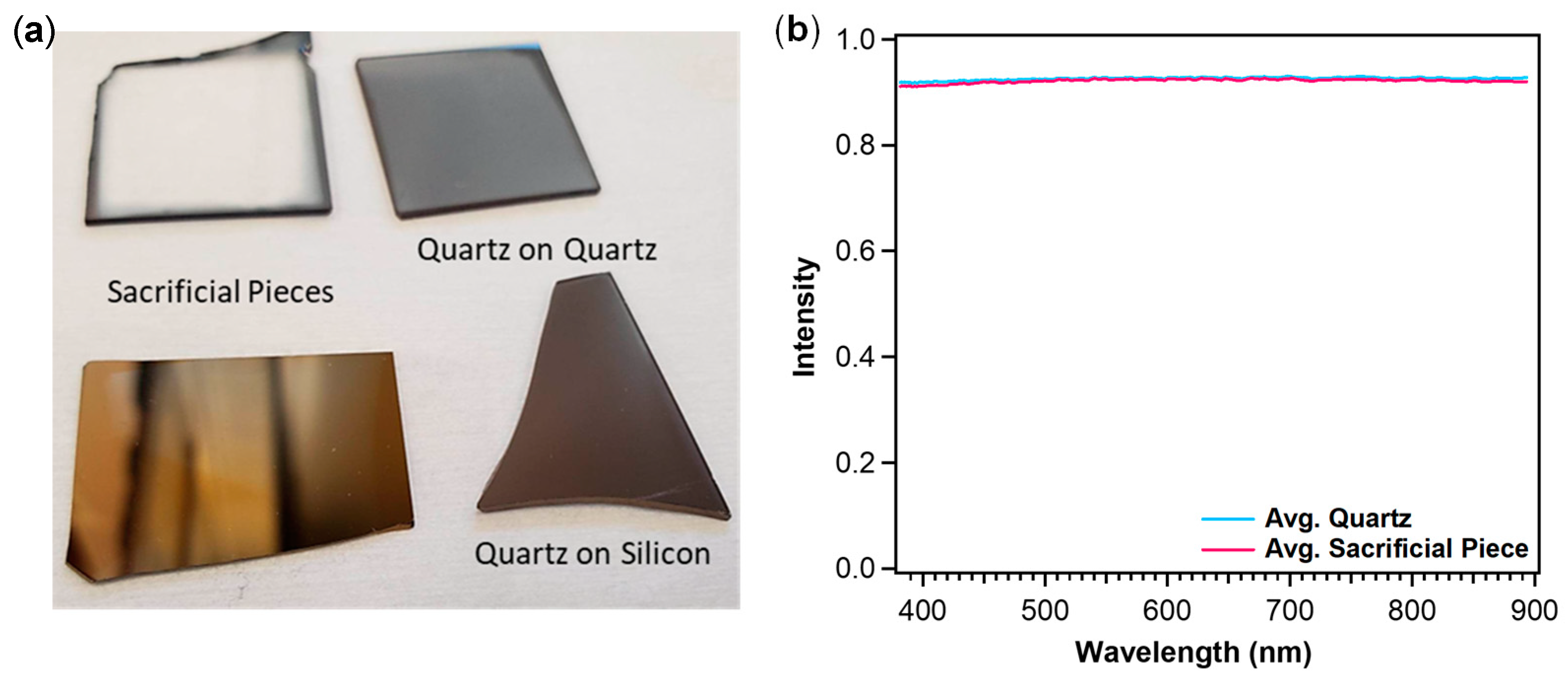
3.1. Producing ALD Films with Single-Side Deposition

The approach we need to use for the extraction of the film’s optical functions requires that deposition be limited to the sample’s top side. One potential method to deal with backside coating is to use Kapton tape. However, adhesive residue is an issue. At temperatures above 300 °C, tape burning and contamination of the films and deposition chamber are major concerns. Instead, a modified sample mounting approach was used, based on the idea of a “sacrificial piece”.
More specifically, target quartz pieces were mounted on top of another quartz piece, or a polished silicon piece, and then the ALD process was executed. The idea behind this approach is that highly polished surfaces in contact limit the free space between the two stacked pieces substantially, which may suppress the conformal nature of the ALD process. Post-deposition, the presence of any backside deposition can be evaluated by performing appropriate measurements on the sacrificial pieces. If backside deposition has been suppressed, then the transmittance of a quartz sacrificial piece should be similar to that of a pristine quartz substrate. Similarly, for a Si sacrificial piece, SE measurements on the contact (top) surface should yield ψ and Δ values similar to those of pristine silicon.
Images and data regarding these samples are shown in Figure 1. Visual inspection (Figure 1a) indicates that there is little to no deposition on the quartz sacrificial piece, except along the edges. The average transmission values of the quartz sacrificial piece match the transmission values of a bare quartz substrate (Figure 1b), suggesting no backside coating on the top quartz piece. In contrast, the Si sacrificial piece shows color variation, indicating the presence of a non-uniform coating. The average ψ and Δ values from the silicon sacrificial piece differ from those of pure silicon at all points on the surface, confirming deposition on the Si sacrificial piece and indicating deposition on the corresponding top quartz piece.
This is further supported by analyzing the respective quartz samples (Figure 1a). The quartz sample mounted on the Si sacrificial piece appears darker, which indicates a larger optical thickness. Transmission measurements confirm this observation: the “quartz on silicon” sample exhibited decreased and non-uniform intensity, which may be due to a greater optical thickness. Based on these observations and measurements, we chose quartz substrates as sacrificial pieces.

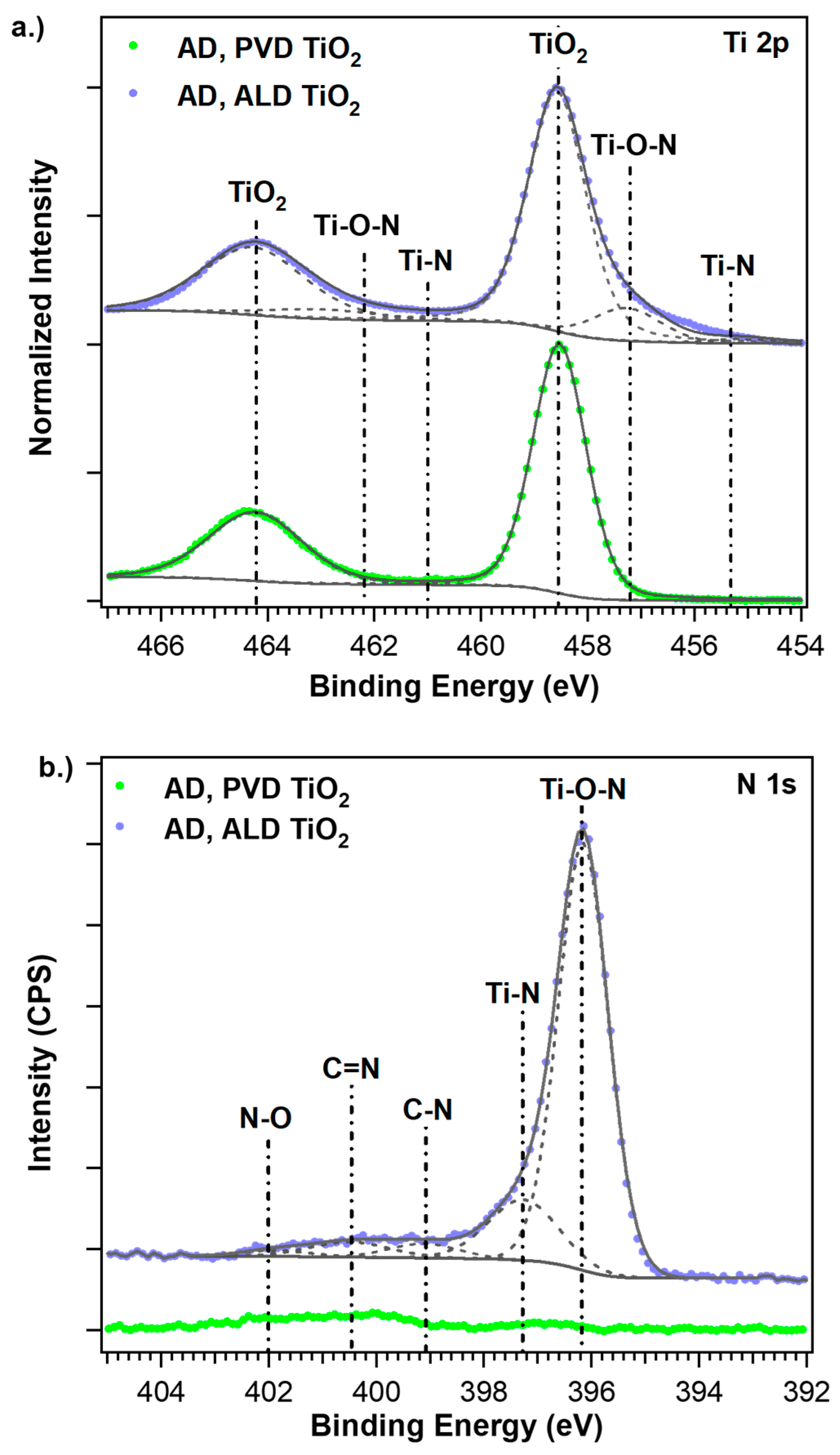
3.2. Composition and Morphology of the Films

The XPS survey scans for a PVD and an ALD sample (Supporting Information, SI, Figure S1) confirm that the films are composed of TiO2 with varying concentrations of carbon and nitrogen-containing impurities. High-resolution spectra (Figure 2) for the Ti 2p region of the PVD TiO2 film (Figure 2a) show the Ti 2p3/2 peak at ~458.5 eV [22] and the Ti 2p1/2 peak at ~464.3 eV, associated with the Ti-O bond in TiO2. ALD films grown at 350 °C with a 5 s purge time are outside the optimal ALD growth window determined for this reactor. These parameters were chosen to further encourage precursor decomposition in a quasi-chemical vapor deposition (CVD) process [23]. With this temperature and purge time, XPS confirmed the presence of Ti-O-N/Ti-N metallic bonding within the films. Specifically, in the Ti 2p region, (Figure 2a), a shoulder is observed in the binding energy range of ~455–457 eV [24] for the as-deposited ALD-grown films. This shoulder is absent in the PVD-grown films. Spectral deconvolution reveals two additional peaks—the feature at ~455 eV is associated with Ti-N bonding, while the peak at 457 eV is associated with TiOxNy [25]. Analysis of the N1s spectral region confirms this assignment.
In the N 1s region (Figure 2b), the corresponding Ti-O-N and Ti-N peaks for the ALD film are observed at 396 and 397 eV, respectively [24], consistent with the peak assignment in the Ti 2p region. The other lower intensity peaks between 399 and 402 eV can be related to chemisorbed nitrogen [24,25] or amine-precursor ligands [26]. The N1s region for the PVD-grown film lacks any spectral features, in agreement with the Ti 2p region.
Composition analysis [27] indicates that the nitrogen (N) content in the films with this type of bonding is ~4.5 atomic percent (at.%) for the 350 °C sample, higher than previously demonstrated [28], and 0% for the PVD TiO2 film. The compositional analysis also shows that the 350 °C film contains 22.8%, 45.9%, and 5.6% of Ti, O, and bonded C, respectively, while the PVD TiO2 film contains 21.3%, 49.6%, and 2.8% of Ti, O, and bonded C, respectively. The remaining atomic percentages in both cases are due to adventitious carbon. The PVD film contains less bonded carbon than the ALD film. This is illustrated by the C 1s region (SI Figure S2), which reveals the presence of carbonate species for both films. Metal oxide films are susceptible to post-deposition reactions with atmospheric moisture and carbon dioxide, forming hydroxycarbonate species [29]. The mid-IR spectrum for the PVD film (SI Figure S3) confirms the presence of carbonate species and adsorbed water from the ambient environment. Since XPS is a surface-sensitive technique, and reactions with atmospheric components are usually limited to the film surface, the measured carbon content for the PVD films should be regarded as an upper limit to the true value. Such small abundances of carbon are typical for all coatings, and the measured optical constants reflect this.
Additionally, high ALD deposition temperatures may result in partial or full film crystallization [30,31]. The far-IR region was used to assess crystallinity, revealing that all films analyzed in this work are mainly amorphous, as evidenced by broad peaks in the spectrum (SI Figure S4). When the 350 °C ALD film is annealed at 900 °C for 10 min in an argon environment, distinct peaks are observed at 181 cm−1, 375 cm−1, and 496 cm−1, indicating the formation of the rutile phase of TiO2 [32]. Previous work [33] has shown that FTIR data are consistent with X-ray diffraction (XRD) results when identifying phases in TiO2 films, supporting FTIR’s reliability for phase distinction in these samples. As a result, observed differences in optical functions can be primarily attributed to compositional differences rather than differences in crystallinity.

3.3. UV–Vis Absorption of the Films

Absorbance data from ultraviolet-visible (UV–Vis) spectroscopy were collected for the ALD and control PVD TiO2 films. Transmittance was calculated from the raw absorbance data and the results are presented in Figure 3. Transmittance values of 100% indicate no absorption, while 0% indicates complete absorption. All ALD films deposited at 350 °C show significant absorption in the visible range. In contrast, the PVD TiO2 film exhibits high transmission, as expected [8,34,35,36]. The high absorption of the ALD TiO2 films can be traced to the presence of the oxynitride metallic bonding [37], confirmed by the XPS measurements. These results confirm that the ALD films are absorbing, necessitating additional information for extracting their optical functions.

3.4. Extracting the Optical Functions of the PVD TiO2 Films

To ensure the validity of the SE + T method, the approach was initially tested on the transparent PVD TiO2. A Cauchy model was used to model conventional ellipsometry measurements on Si (100) and for the SE + T approach on quartz. Both techniques returned similar values for the optical functions (Figure 4), with only slight differences at the lower wavelengths. The reported values for the refractive index (Figure 4, green) can vary [38,39] at lower wavelengths due to differences in substrates and film growth [40]. The extinction coefficient (Figure 4, orange) is zero for the visible wavelengths [41,42,43], but nonzero at ~400 nm, which is accurately described with both techniques.
The Cauchy fitting parameters (Table 2) obtained for both methods are similar. The thickness results are consistent with the measured profilometer thickness. For thick samples, such as those in this work, MSE values around 10 are acceptable [21]. This benchmarks the SE + T method and ensures that SE + T can be used to determine accurate optical constants for the absorbing ALD TiO2 films.

3.5. Extracting the Optical Functions of the ALD TiO2 Films

While the SE + T method is compatible with the ALD process and provides reasonable results for transparent films, it must be tested rigorously for absorbing films. This validation can be conducted by preparing samples with varied thicknesses (controlled by the number of ALD cycles) at 350 °C with a 5 s purge and testing the sensitivity across three ALD samples. If there is no backside deposition and the SE + T measurements and modeling can (i) simultaneously fit all ψ, Δ, and T measurements, (ii) accurately map thickness variations when compared to profilometry measurements, and (iii) yield a low MSE, then it is expected to provide reliable optical functions.
When operating outside the optimal ALD conditions, and especially at elevated temperatures, there may be significant precursor decomposition, resulting in thickness variations across the samples. To ensure consistency between the quartz and silicon measurements, we mounted quartz (on quartz SPs) and Si pieces side by side on the sample holder. Samples named “A” have been placed downstream of samples named “B” on the sample holder for each deposition. For samples with no backside deposition, we evaluated the optical properties and thickness across three equivalent “spots” with multiple measurements for each spot. Sample fits of the SE and T experimental data are shown in Figure 5.
The simple graded B-spline optical model can fit the experimental data accurately, as the model-generated data lie on top of the measured data set, reproducing all the structures and features simultaneously. The thickness obtained from the SE + T measurements and the model on quartz can now be cross-checked with profilometer measurements on Si (100), as shown in Table 3.
Considering the uncertainties, the SE + T thickness measurements on quartz and the profilometry thickness measurements on Si (100) are within approximately 5%. Additionally, we observe that the films downstream (ALD 2A) are thinner than the films upstream (ALD 2B), as shown by both profilometer measurements and optical modeling on SE + T data. This consistency supports the reliability of the SE + T method and the optical model used.
The optical functions between 380 and 900 nm for the three ALD samples are presented in Figure 6. The best fit for the data is obtained by assuming that the film is graded, with a non-constant index of refraction throughout the film bulk. Specifically, the film is divided into five sublayers, each with a linearly varying index of refraction. An average extinction coefficient is assumed for all layers, as varying it linearly does not improve the fit quality. Similar ALD films containing oxynitride bonds have been shown to exhibit a depth-varying composition due to ambient oxidation, validating the assumption of a varying index of refraction with film depth [28]. In contrast, grading the film did not change the optical functions of the as-deposited PVD TiO2 films (Figure 6).
Comparing these results to the known physical characteristics of the samples can aid in evaluating the results. The ALD films contain TiO2, TiOxNy, and TiN, as confirmed by XPS, and absorb in the visible range, as confirmed by UV–Vis. This suggests that their optical functions should differ from those of PVD TiO2, which is indeed observed. The PVD TiO2 films (Figure 6a, green) have the highest n of the films in this work and k = 0 in the visible range (Figure 6b, green), consistent with their measured high purity and their high transparency in the visible range.
For the ALD films, n decreases with wavelength until about 600 nm, then increases as a function of wavelength, while k only increases with wavelength. The measured refractive index n is somewhat higher and the extinction coefficient is somewhat lower than those reported for TiN films in the literature. Our films contain only about 4.5 at.% of Ti-N bonding, significantly less than the films in the literature. Thus, overall, the optical functions are consistent with the composition of the films and the literature references [44]. Additionally, a lower n is measured for the bottom layers, which is compatible with a more TiN-like (greater oxynitride concentration) bottom layer, matching experimental observations [28].
These results capture the physical behavior of the ALD films, falling within the expected range between pure TiO2 and pure TiN, as expected for this composition. Furthermore, the resulting MSE values are less than 3, which is reasonable for our experimental data. This further supports the reliability of the mounting approach, optical modeling, and resulting optical functions.

4. Conclusions

Single-angle spectroscopic ellipsometry is inadequate for extracting the optical functions of absorbing films because it provides an insufficient number of measurable parameters. Additionally, absorbing films deposited by ALD may also have backside deposition, which further complicates their optical characterization. To address these challenges, we used the SE + T technique in conjunction with a sample mounting approach that effectively eliminates backside deposition, allowing for the accurate determination of the film’s optical functions and thickness. The method yields realistic optical functions and thickness values, which are validated by independent techniques.

Supplementary Materials

The following supporting information can be downloaded at https://www.mdpi.com/article/10.3390/coatings14121555/s1, Figure S1: Wide survey results for as-deposited ALD and PVD TiO2 films; Figure S2: C 1s results for as-deposited ALD and PVD TiO2 films. Sample fits are shown in grey. The PVD film shows less bonded carbon than the ALD film; Figure S3: Mid-IR results (4000–1200 cm−1) for the as-deposited PVD TiO2 film; Figure S4: Far-IR results (600–75 cm−1) for the as-deposited ALD and PVD TiO2 films and annealed ALD film.

Author Contributions

Conceptualization, N.K.C. and T.G.; formal analysis, N.K.C. and T.G.; funding acquisition, T.G.; methodology, N.K.C. and T.G.; supervision, T.G.; validation, N.K.C.; writing—original draft, N.K.C.; writing—review and editing, T.G. All authors have read and agreed to the published version of the manuscript.

Funding

This research was funded by the National Science Foundation (NSF) grant number DMR-1905305.

Institutional Review Board Statement

Not applicable.

Informed Consent Statement

Not applicable.

Data Availability Statement

The raw data supporting the conclusions of this article may be obtained from the authors upon reasonable request.

Acknowledgments

We thank Andrea Donohue from the Woollam facility for her time and help with the optical models. We also thank Lisa Kelly and her graduate students from the Department of Chemistry and Biochemistry at UMBC for their help in obtaining UV–Vis data; Ilkeun Lee at the University of California, Riverside; and Karen Gaskell at the University of Maryland, College Park, for taking the XPS data. We would also like to thank Erik Crowe in the Physics Department at UMBC for machining the sample holder and transmission mounts. Student support provided by an NIGMS Graduate Research Training Initiative for Student Enhancement (G-RISE) Grant (T32-GM144876) is acknowledged. This material is based upon work supported by the National Science Foundation (NSF) under grant DMR-1905305.

Conflicts of Interest

The authors declare no conflicts of interest.

References

  1. Yu, X.; Marks, T.J.; Facchetti, A. Metal Oxides for Optoelectronic Applications. Nat. Mater. 2016, 15, 383–396. [Google Scholar] [CrossRef] [PubMed]
  2. Choy, K.L. Chemical Vapour Deposition of Coatings. Prog. Mater. Sci. 2003, 48, 57–170. [Google Scholar] [CrossRef]
  3. Kaliyannan, G.V.; Palanisamy, S.V.; Priyanka, E.B.; Thangavel, S.; Sivaraj, S.; Rathanasamy, R. Investigation on Sol-Gel Based Coatings Application in Energy Sector—A Review. Mater. Today Proc. 2021, 45, 1138–1143. [Google Scholar] [CrossRef]
  4. Mozumder, M.S.; Mourad, A.-H.I.; Pervez, H.; Surkatti, R. Recent Developments in Multifunctional Coatings for Solar Panel Applications: A Review. Sol. Energy Mater. Sol. Cells 2019, 189, 75–102. [Google Scholar] [CrossRef]
  5. George, S.M. Atomic Layer Deposition: An Overview. Chem. Rev. 2010, 110, 111–131. [Google Scholar] [CrossRef]
  6. Detavernier, C.; Dendooven, J.; Sree, S.P.; Ludwig, K.F.; Martens, J.A. Tailoring Nanoporous Materials by Atomic Layer Deposition. Chem. Soc. Rev. 2011, 40, 5242–5253. [Google Scholar] [CrossRef]
  7. Ristok, S.; Flad, P.; Giessen, H. Atomic Layer Deposition of Conformal Anti-Reflective Coatings on Complex 3D Printed Micro-Optical Systems. Opt. Mater. Express 2022, 12, 2063. [Google Scholar] [CrossRef]
  8. Wang, X.; Wu, G.; Zhou, B.; Shen, J. Optical Constants of Crystallized TiO2 Coatings Prepared by Sol-Gel Process. Materials 2013, 6, 2819–2830. [Google Scholar] [CrossRef]
  9. Shamma, K.; Aldwayyan, A.; Albrithen, H.; Alodhayb, A. Exploiting the Properties of TiO2 Thin Films as a Sensing Layer on (MEMS)-Based Sensors for Radiation Dosimetry Applications. AIP Adv. 2021, 11, 025209. [Google Scholar] [CrossRef]
  10. Hilfiker, J.N.; Singh, N.; Tiwald, T.; Convey, D.; Smith, S.M.; Baker, J.H.; Tompkins, H.G. Survey of Methods to Characterize Thin Absorbing Films with Spectroscopic Ellipsometry. Thin Solid Films 2008, 516, 7979–7989. [Google Scholar] [CrossRef]
  11. Rafieian, D.; Ogieglo, W.; Savenije, T.; Lammertink, R.G.H. Controlled Formation of Anatase and Rutile TiO2 Thin Films by Reactive Magnetron Sputtering. AIP Adv. 2015, 5, 097168. [Google Scholar] [CrossRef]
  12. Zeiss, C. Application of the Tauc-Lorentz Formulation to the Interband Absorption of Optical Coating Materials. Appl. Opt. 2001, 41, 3137–3141. [Google Scholar]
  13. Wang, L.; Liu, H.; Li, S.; Jiang, C.; Ji, Y.; Chen, D. Study on the Composite Dispersion Model of Optical Constants of Metal-Oxide Films in the Range from Ultraviolet to near Infrared. Optik 2018, 168, 892–900. [Google Scholar] [CrossRef]
  14. Hilfiker, J.N.; Linford, M.R. Fitting the Spectroscopic Ellipsometry Data from a Rather Thick (Organic?) Film on Fused Silica. Vac. Technol. Coat. 2021, 22, 34–38. [Google Scholar]
  15. Hilfiker, J.N.; Linford, M.R. Combining Spectroscopic Ellipsometry and Transmission Spectrophotometric Data for the Analysis of Thin Metal Films. Vac. Technol. Coat. 2022, 23, 33–37. [Google Scholar]
  16. Hackley, J.C.; Gougousi, T.; Demaree, J.D. Nucleation of HfO2 Atomic Layer Deposition Films on Chemical Oxide and H-Terminated Si. J. Appl. Phys. 2007, 102, 034101. [Google Scholar] [CrossRef]
  17. Ylilammi, M. Monolayer Thickness in Atomic Layer Deposition. Thin Solid Films 1996, 279, 124–130. [Google Scholar] [CrossRef]
  18. Becker, J.S.; Kim, E.; Gordon, R.G. Atomic Layer Deposition of Insulating Hafnium and Zirconium Nitrides. Chem. Mater. 2004, 16, 3497–3501. [Google Scholar] [CrossRef]
  19. Hausmann, D.M.; de Rouffignac, P.; Smith, A.; Gordon, R.; Monsma, D. Highly Conformal Atomic Layer Deposition of Tantalum Oxide Using Alkylamide Precursors. Thin Solid Films 2003, 443, 1–4. [Google Scholar] [CrossRef]
  20. Synowicki, R.A. Suppression of Backside Reflections from Transparent Substrates. Phys. Status Solidi C 2008, 5, 1085–1088. [Google Scholar] [CrossRef]
  21. J.A. Woollam Co., Inc. CompleteEASE Data Analysis Manual 2011; J.A. Woollam Co., Inc.: Lincoln, NE, USA, 2011. [Google Scholar]
  22. Stefanov, P.; Shipochka, M.; Stefchev, P.; Raicheva, Z.; Lazarova, V.; Spassov, L. XPS Characterization of TiO2 Layers Deposited on Quartz Plates. J. Phys. Conf. Ser. 2008, 100, 012039. [Google Scholar] [CrossRef]
  23. Driessen, J.P.A.M.; Schoonman, J.; Jensen, K.F. Infrared Spectroscopic Study of Decomposition of Ti(N(CH3)2)4. J. Electrochem. Soc. 2001, 148, G178–G184. [Google Scholar] [CrossRef]
  24. Song, X.; Gopireddy, D.; Takoudis, C.G. Characterization of Titanium Oxynitride Films Deposited by Low Pressure Chemical Vapor Deposition Using Amide Ti Precursor. Thin Solid Films 2008, 516, 6330–6335. [Google Scholar] [CrossRef]
  25. Khwansungnoen, P.; Chaiyakun, S.; Rattana, T. Room Temperature Sputtered Titanium Oxynitride Thin Films: The Influence of Oxygen Addition. Thin Solid Films 2020, 711, 138269. [Google Scholar] [CrossRef]
  26. Olayo, M.G.; Alvarado, E.J.; González-Torres, M.; Gómez, L.M.; Cruz, G.J. Quantifying Amines in Polymers by XPS. Polym. Bull. 2024, 81, 2319–2328. [Google Scholar] [CrossRef]
  27. Shard, A.G. Practical Guides for X-Ray Photoelectron Spectroscopy: Quantitative XPS. J. Vac. Sci. Technol. A 2020, 38, 041201. [Google Scholar] [CrossRef]
  28. Kuis, R.; Gougousi, T.; Basaldua, I.; Burkins, P.; Kropp, J.A.; Johnson, A.M. Engineering of Large Third-Order Nonlinearities in Atomic Layer Deposition Grown Nitrogen-Enriched TiO2. ACS Photonics 2019, 6, 2966–2973. [Google Scholar] [CrossRef]
  29. Gougousi, T.; Parsons, G. Postdeposition Reactivity of Sputter-Deposited High-Dielectric-Constant Films with Ambient H2O and Carbon-Containing Species. J. Appl. Phys. 2004, 95, 1391–1396. [Google Scholar] [CrossRef]
  30. Aarik, J.; Aidla, A.; Uustare, T.; Sammelselg, V. Morphology and Structure of TiO2 Thin Films Grown by Atomic Layer Deposition. J. Cryst. Growth 1995, 148, 268–275. [Google Scholar] [CrossRef]
  31. Kim, S.K.; Hoffmann-Eifert, S.; Reiners, M.; Waser, R. Relation Between Enhancement in Growth and Thickness-Dependent Crystallization in ALD TiO2 Thin Films. J. Electrochem. Soc. 2010, 158, D6. [Google Scholar] [CrossRef]
  32. Schöche, S.; Hofmann, T.; Korlacki, R.; Tiwald, T.E.; Schubert, M. Infrared Dielectric Anisotropy and Phonon Modes of Rutile TiO2. J. Appl. Phys. 2013, 113, 164102. [Google Scholar] [CrossRef]
  33. Henegar, A.J.; Gougousi, T. Stability and Surface Reactivity of Anatase TiO2 Films. ECS J. Solid State Sci. Technol. 2015, 4, P298–P304. [Google Scholar] [CrossRef]
  34. Abdel-Aziz, M.M.; Yahia, I.S.; Wahab, L.A.; Fadel, M.; Afifi, M.A. Determination and Analysis of Dispersive Optical Constant of TiO2 and Ti2O3 Thin Films. Appl. Surf. Sci. 2006, 252, 8163–8170. [Google Scholar] [CrossRef]
  35. Ghrairi, N.; Bouaicha, M. Structural, Morphological, and Optical Properties of TiO2 Thin Films Synthesized by the Electro Phoretic Deposition Technique. Nanoscale Res. Lett. 2012, 7, 357. [Google Scholar] [CrossRef] [PubMed]
  36. Sreemany, M.; Sen, S. A Simple Spectrophotometric Method for Determination of the Optical Constants and Band Gap Energy of Multiple Layer TiO2 Thin Films. Mater. Chem. Phys. 2004, 83, 169–177. [Google Scholar] [CrossRef]
  37. Demeter, A.; Samoila, F.; Tiron, V.; Stanescu, D.; Magnan, H.; Straticiuc, M.; Burducea, I.; Sirghi, L. Visible-Light Photocatalytic Activity of TiOxNy Thin Films Obtained by Reactive Multi-Pulse High Power Impulse Magnetron Sputtering. Surf. Coat. Technol. 2017, 324, 614–619. [Google Scholar] [CrossRef]
  38. Mosaddeq-ur-Rahman, M.; Yu, G.; Soga, T.; Jimbo, T.; Ebisu, H. Umeno Refractive Index and Degree of Inhomogeneity of Nanocrystalline TiO2 Thin Films: Effects of Substrate and Annealing Temperature. J. Appl. Phys. 2000, 88, 9. [Google Scholar] [CrossRef]
  39. Kasikov, A.; Aarik, J.; Mändar, H.; Moppel, M.; Pärs, M.; Uustare, T. Refractive Index Gradients in TiO2 Thin Films Grown by Atomic Layer Deposition. J. Phys. Appl. Phys. 2006, 39, 54–60. [Google Scholar] [CrossRef]
  40. Jolivet, A.; Labbé, C.; Frilay, C.; Debieu, O.; Marie, P.; Horcholle, B.; Lemarié, F.; Portier, X.; Grygiel, C.; Duprey, S.; et al. Structural, Optical, and Electrical Properties of TiO2 Thin Films Deposited by ALD: Impact of the Substrate, the Deposited Thickness and the Deposition Temperature. Appl. Surf. Sci. 2023, 608, 155214. [Google Scholar] [CrossRef]
  41. Saha, D.; Ajimsha, R.S.; Rajiv, K.; Mukherjee, C.; Gupta, M.; Misra, P.; Kukreja, L.M. Spectroscopic Ellipsometry Characterization of Amorphous and Crystalline TiO2 Thin Films Grown by Atomic Layer Deposition at Different Temperatures. Appl. Surf. Sci. 2014, 315, 116–123. [Google Scholar] [CrossRef]
  42. Kim, S.Y. Simultaneous Determination of Refractive Index, Extinction Coefficient, and Void Distribution of Titanium Dioxide Thin Film by Optical Methods. Appl. Opt. 1996, 35, 6703–6707. [Google Scholar] [CrossRef] [PubMed]
  43. Mardare, D.; Stancu, A. On the Optical Constants of TiO2 Thin Films. Ellipsometric Studies. Mater. Res. Bull. 2000, 35, 2017–2025. [Google Scholar] [CrossRef]
  44. Ali, S.; Magnusson, R.; Pshyk, O.; Birch, J.; Eklund, P.; Le Febvrier, A. Effect of O/N Content on the Phase, Morphology, and Optical Properties of Titanium Oxynitride Thin Films. J. Mater. Sci. 2023, 58, 10975–10985. [Google Scholar] [CrossRef]
Figure 1. (a) Image of post-deposition samples and sacrificial pieces. (b) Average transmission measurement through a quartz sacrificial piece compared with average quartz substrate transmission intensity.
Coatings 14 01555 g001
Figure 2. (a) Ti 2p region and (b) N 1s region for as-deposited ALD (350 °C) and PVD-grown TiO2 samples. Sample fits are included for the peaks in gray.
Coatings 14 01555 g002
Figure 3. UV–Vis data for a series of TiO2 films. The data for a quartz substrate are shown for reference.
Coatings 14 01555 g003
Figure 4. The optical functions for the PVD TiO2 films on Si and quartz.
Coatings 14 01555 g004
Figure 5. Simultaneously fitted (a) SE transmission (T) data and (b) SE Psi/Delta (ψ, Δ) data for the samples ALD 1 and ALD 2. The colored solid and dashed lines show the measured experimental data, and the black dashed lines show the model fit.
Coatings 14 01555 g005
Figure 6. Optical functions: (a) refractive index n, and (b) extinction coefficient k obtained using the SE + T approach with a graded B-spline model for the absorbing ALD TiO2 films and a Cauchy model for the transparent PVD TiO2 film. The top layer is represented by a solid line while the bottom layer is shown by a dashed line of the same color for each sample.
Coatings 14 01555 g006
Table 1. Summary of ALD-deposited samples. Samples marked “A” are downstream and samples marked “B” are upstream.
Sample NameNumber of CyclesTemperature (°C)Purge (s)
ALD 12853505
ALD 2A, B3503505
Table 2. Summary of fit parameters for PVD TiO2 films using the Cauchy model.
Sample SubstrateABCModel Thickness (nm)Surface Roughness (nm)n @ 632.8 nmMSEThickness (Profilometer) (nm)
Silicon2.270.0310.005891.1 ± 0.1 2.6 ± 0.12.387.996.0 ± 3.8
Quartz2.280.0150.007192.7 ± 0.1 4.0 ± 0.12.368.3
Table 3. SE + T on quartz and profilometry on Si (100) results for ALD TiO2 film at 350 °C.
Sample NameSE + T
Spot 1 (nm)
Profilometer Spot 1 (nm)SE + T
Spot 2 (nm)
Profilometer Spot 2 (nm)SE + T
Spot 3 (nm)
Profilometer Spot 3 (nm)
ALD 139.1 ± 0.3 41.8 ± 0.8 40.0 ± 0.1 41.2 ± 1.4 N/AN/A
ALD 2A49.9 ± 0.1 49.6 ± 0.9 49.1 ± 0.1 49.0 ± 0.4 48.2 ± 0.1 50.1 ± 0.6
ALD 2B65.1 ± 0.1 67.7 ± 1.3 64.5 ± 0.1 62.2 ± 1.0 62.6 ± 0.1 61.6 ± 0.8
Disclaimer/Publisher’s Note: The statements, opinions and data contained in all publications are solely those of the individual author(s) and contributor(s) and not of MDPI and/or the editor(s). MDPI and/or the editor(s) disclaim responsibility for any injury to people or property resulting from any ideas, methods, instructions or products referred to in the content.

