3.1. Chemical Compositions and Phase Structures of ZrBSiTa and (ZrBSiTa)Nx Films
Table 1 lists the chemical compositions of as-deposited ZrBSiTa and (ZrBSiTa)N
x films. The Si content revealed an increasing trend with increasing P
Si. In contrast, the Zr, B, and Ta contents demonstrated a decreasing trend with increasing P
Si for each batch sample, which implied that the sputtering yield of these sputter guns in the cosputtering apparatus was independent. The N content of batch B films decreased from 59.4 at.% to 54.5, 54.6, and 51.4 at.% as increasing P
Si from 0 to 50, 100, and 150 W, whereas the N content of the batch C and D samples remained constant at 61.4–64.6 and 63.0–63.5 at.%, respectively. For example, the batch D samples exhibited chemical compositions of Zr
10B
9Ta
18N
63, Zr
7B
6Si
10Ta
13N
64, Zr
5B
6Si
17Ta
9N
63, and Zr
4B
4Si
21Ta
8N
63 when the applied P
Si was 0, 50, 100, and 150 W, respectively, which were accompanied by a deposition rate increasing from 4.7 to 5.7, 6.9, and 8.1 nm/min, respectively. The stoichiometric ratio (
x) was higher than 1 for all the (ZrBSiTa)N
x films. However, in a previous study [
36], the value of
x was less than 0.5 for (NbTaMoW)N
x films, even for the sample fabricated under a high R
N2 value of 0.4. This variation was attributed to the evident difference in affinity between N and the other elements. Mo
2N and W
2N are the preferentially formed Mo–N and W–N compounds during sputtering. The standard formation enthalpies for BN, TaN, ZrN, Si
3N
4, TaB
2, and ZrB
2 at 298 K are −254.4, −252.3, −365.3, −744.8, −209.2, and −322.6 kJ/mol [
37], respectively. N should preferentially bond to Zr and then bond to B, Ta, and Si, whereas B should preferentially bond to N, Zr, and Ta. Moreover, the ZrN, BN, and TaN had a stoichiometric ratio of 1, whereas the
x value is 1.33 for Si
3N
4. Therefore, the
x values were >1 for all the (ZrBSiTa)N
x films. ZrB
y, as well as TiB
y [
38], tended to form overstoichiometric diboride thin films through sputtering [
26]. In our previous study [
39], a ZrB
2.5 (28.4% Zr–70.5% B–1.1% O) film was fabricated using a ZrB
2 target. However, all the ZrBSiTa and (ZrBSiTa)N
x films had understoichiometric B/Zr ratios of 0.9–1.6, which could be attributed to scattering and resputtering of light B atoms during cosputtering [
26].
Table 2 lists the thicknesses and deposition rates of the fabricated ZrBSiTa and (ZrBSiTa)N
x films. The deposition rate increased with the increasing P
Si level for all the films. The deposition rate decreased with increasing R
N2, which was attributed to the target poisoning effect [
40] and the low sputtering efficiency of N correlated to that of Ar ions [
41,
42]. For example, the deposition rates for the Zr
10B
11Ta
19N
60 (B1), Zr
9B
12Ta
14N
65 (C1), and Zr
10B
9Ta
18N
63 (D1) samples decreased from 10.7 to 6.6 and 4.7 nm/min as R
N2 increased from 0.1 to 0.2 and 0.4.
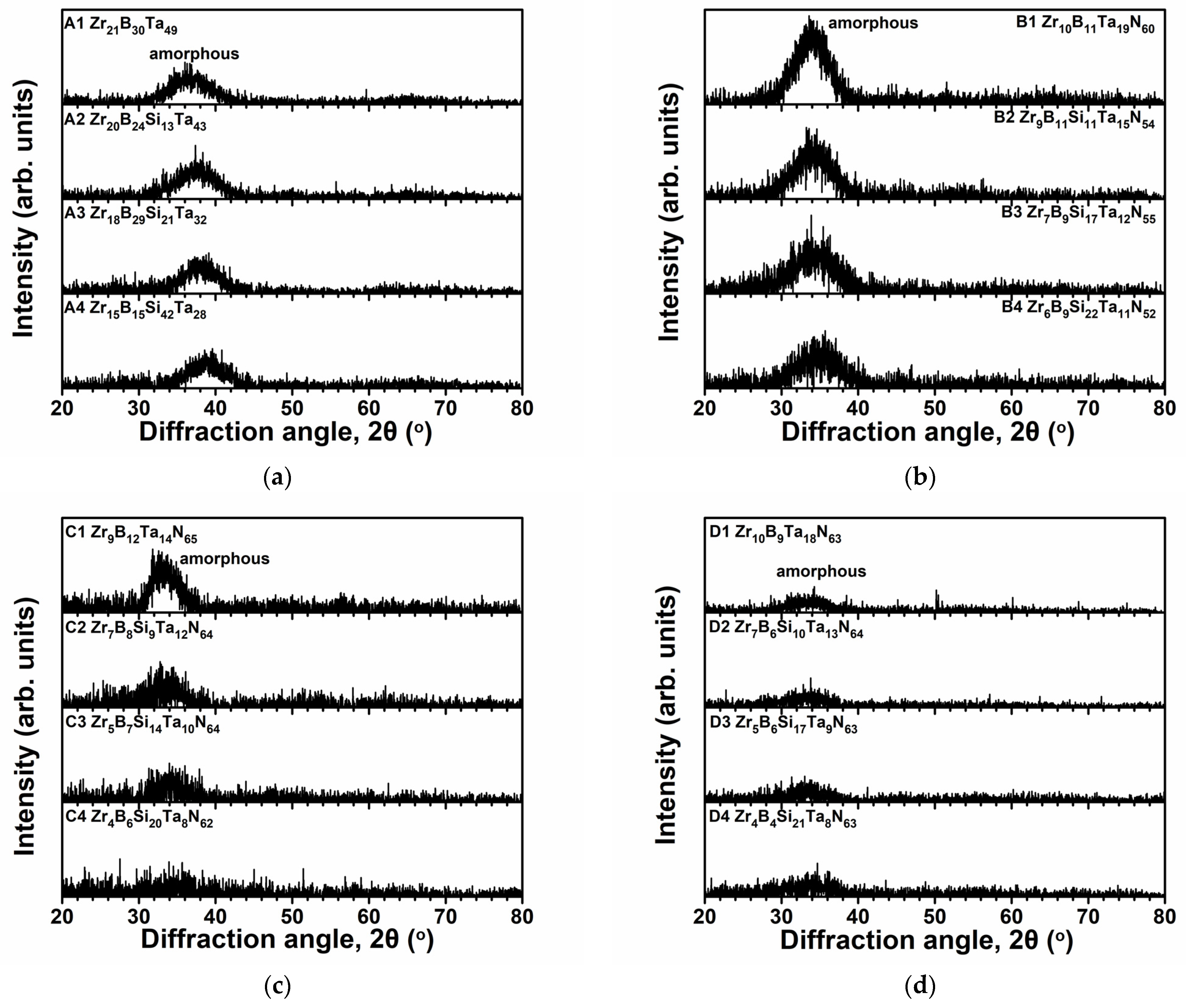
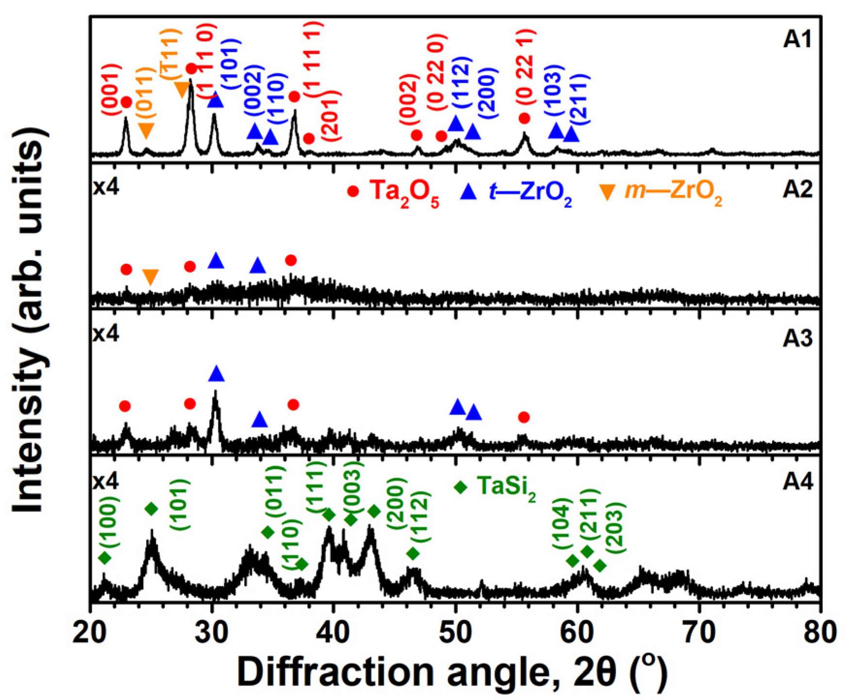
Figure 1 displays the GIXRD patterns of the as-fabricated ZrBSiTa and (ZrBSiTa)N
x Films. The broad peaks observed at 2θ of 36–38° for ZrBSiTa films and at 2θ of 34° for (ZrBSiTa)N
x films indicated that all the as-fabricated ZrBSiTa and (ZrBSiTa)N
x films formed amorphous structures. In our previous study [
43], TaZrN films crystallized into a face-centered cubic phase and revealed a columnar structure. The addition of B and Si into TaZrN films affected the phase structures. Multicomponent alloys could form distinct structures (solid solution, intermediate phase, and bulk metallic glasses) depending on their atomic size difference (
δ), mixing enthalpy (Δ
Hmix), and mixing entropy (Δ
Smix) [
44]. Multicomponent bulk metallic glasses have larger
δ (6%–18%) and more negative Δ
Hmix (−25–−37 kJ/mol) [
44]. The batch A (ZrBSiTa) samples exhibited high
δ values of 24.0%, 22.6%, 24.2%, and 19.6%, significant and negative Δ
Hmix values of −48, −58, −65, and −66 kJ/mol, and medium mixing entropy values of 8.6, 10.7, 11.3, and 10.7 J/K.mol for Zr
21B
30Ta
49 (A1), Zr
20B
24Si
13Ta
43 (A2), Zr
18B
29Si
21Ta
32 (A3), and Zr
15B
15Si
42Ta
28 (A4), respectively, which resulted in forming amorphous structures. Moreover, sputtered BN [
28,
29] and SiN
x films tended to be amorphous, which resulted in the formation of amorphous structures for the (ZrBSiTa)N
x films.
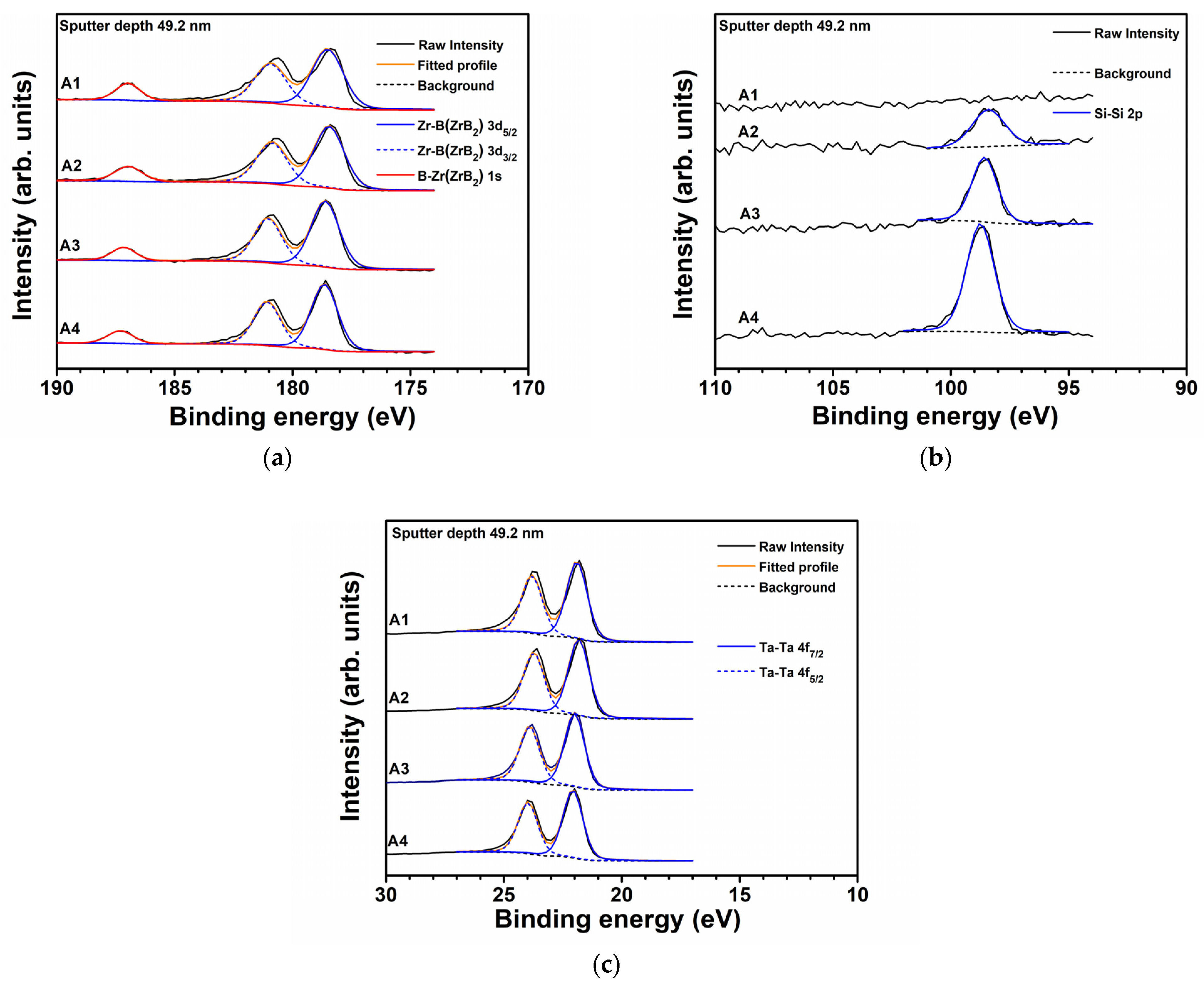
Figure 2 displays the XPS spectra and curve fitting of Zr 3d, B 1s, Si 2p, and Ta 4f for the batch A samples at a sputter depth of 49.2 nm. The XPS analysis results of batch A samples at sputter depths of 16.4–49.2 nm are listed in
Table 3. The binding energies of Zr 3d
5/2 at 178.49–178.70 eV were recognized as Zr–B bonds in a ZrB
2 compound. The B 1s signals were determined at 187.01–187.33 eV, identified as B–Zr bonds. The reported Zr 3d
5/2 and B 1s binding energies for an epitaxial ZrB
2 film were 178.9 and 187.9 eV [
45], respectively. The binding energy of Si–Si bonds was 98.43–98.77 eV. The binding energy of Ta 4f
7/2 for the Ta–Ta bonds was 21.88–22.08 eV, comparable to metallic Ta at 21.9 eV [
32]. The Zr 3d
5/2 was also reported to be 178.8 eV in ZrSi
2 [
46]. However, the standard formation enthalpy of ZrSi
2 at 298 K is −159.4 kJ/mol [
32], which is lower than that of ZrB
2. ZrSi
2 should be not the preferentially formed compound.
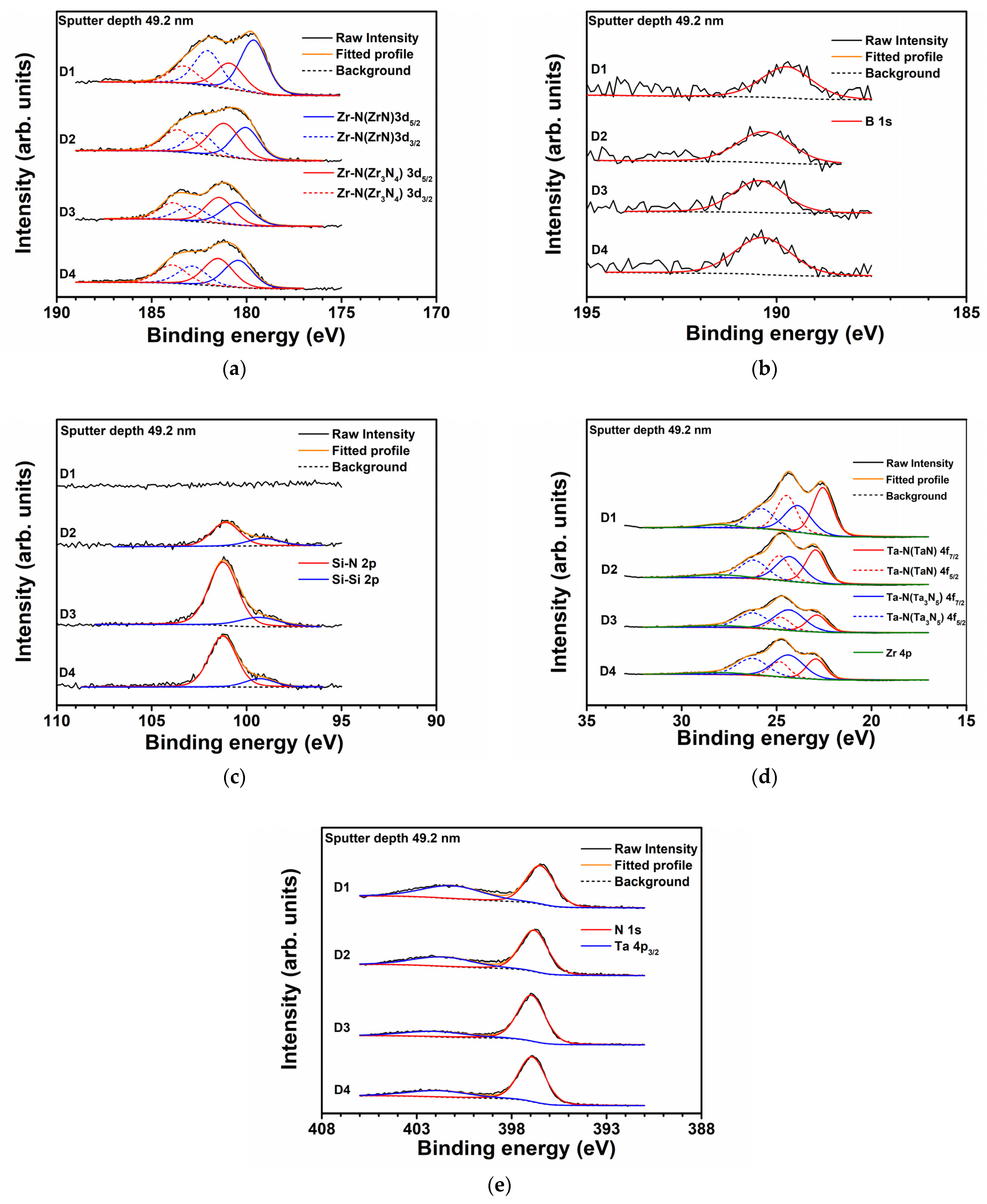
Figure 3 displays the XPS spectra of Zr 3d, B 1s, Si 2p, Ta 4f, and N 1s core levels for batch D films at a depth of 49.2 nm.
Table 4 lists the XPS analysis results of the batch D samples at sputter depths of 16.4–49.2 nm.
Figure 3a shows the curve fitting of the Zr profiles, which were split into two 3d doublets, representing Zr–N bonds for ZrN and Zr
3N
4 components. The average Zr 3d
5/2 values at sputter depths of 16.4–49.2 nm were 179.60–180.52 and 180.84–181.46 eV, respectively. The B 1s signals of 189.74–190.44 eV were identified as B–N bonds comparable with reported values of 190.3 eV [
28,
47]. The Si signals of the Zr
7B
6Si
10Ta
13N
64, Zr
5B
6Si
17Ta
9N
63, and Zr
4B
4Si
21Ta
8N
63 films comprised two components whose binding energies were 99.02–99.34 and 101.15–101.28 eV for the Si–Si and Si–N bonds, respectively. Previous studies [
32,
48,
49] have reported Si 2p signals at 99.2, 101.80, 102.60, and 103–103.50 eV to be Si–Si, Si–N, Si–N–O, and Si–O bonds, respectively. Therefore, only Si–N and Si–Si bonds were detected for the batch D films.
Figure 3d shows the Ta signals, split into two 4f doublets, representing Ta–N bonds for TaN and Ta
3N
5. The Ta 4f
7/2 signals were determined at 22.56–22.95 and 23.89–24.38 eV for TaN and Ta
3N
5, respectively, which were comparable with reported 22.2–23.0 [
50,
51] and 24.2 [
52] eV. All the aforementioned binding energies of the Zr
10B
9Ta
18N
63 (D1) sample were lower than those of the Zr
7B
6Si
10Ta
13N
64, Zr
5B
6Si
17Ta
9N
63, and Zr
4B
4Si
21Ta
8N
63 samples, which could be attributed to a charge effect for the Si-containing films with high resistivity.
3.3. Thermal Stability of ZrBSiTa and ZrBSiTaN Films
The thermal stability tests were performed at 800 and 900 °C within purged Ar gas in an RTA furnace.
Figure 5 shows the GIXRD patterns of the ZrBSiTa films after 10 min annealing at 800 °C, which exhibits the formation of tetragonal ZrO
2 (
t-ZrO
2) (ICDD 00-042-1164); monoclinic ZrO
2 (
m-ZrO
2) (ICDD 00-037-1484); and orthorhombic Ta
2O
5 (ICDD 00-025-0922) phases for the annealed Zr
21B
30Ta
49 (A1), Zr
20B
24Si
13Ta
43 (A2), and Zr
18B
29Si
21Ta
32 (A3) films. A TaSi
2 (ICDD 00-038-0483) phase was observed for the annealed Zr
15B
15Si
42Ta
28 (A4) film with a high Si content. The O originated from the residual contamination in the chamber. The SiO
2 and B
2O
3 which was possibly present should be amorphous and not shown in these XRD patterns. The aforementioned four ZrBSiTa films were annealed at the same time, which implied that Zr
15B
15Si
42Ta
28 had higher oxidation resistance among the ZrBSiTa films. In contrast, all the (ZrBSiTa)N
x films maintained an amorphous phase in their GIXRD patterns after 10 min annealing at 800 °C. After extending the annealing time to 20 and 30 min, all the (ZrBSiTa)N
x films were amorphous except for the Zr
9B
12Ta
14N
65 (C1) and Zr
10B
9Ta
18N
63 (D1) films. The C1 and D1 samples exhibited ZrO
2 and Ta
2O
5 phases after 30 and 20 min annealing, respectively.
Table 6 lists the XRD analysis results of the ZrBSiTa and (ZrBSiTa)N
x films annealed at 800 and 900 °C in Ar gas.
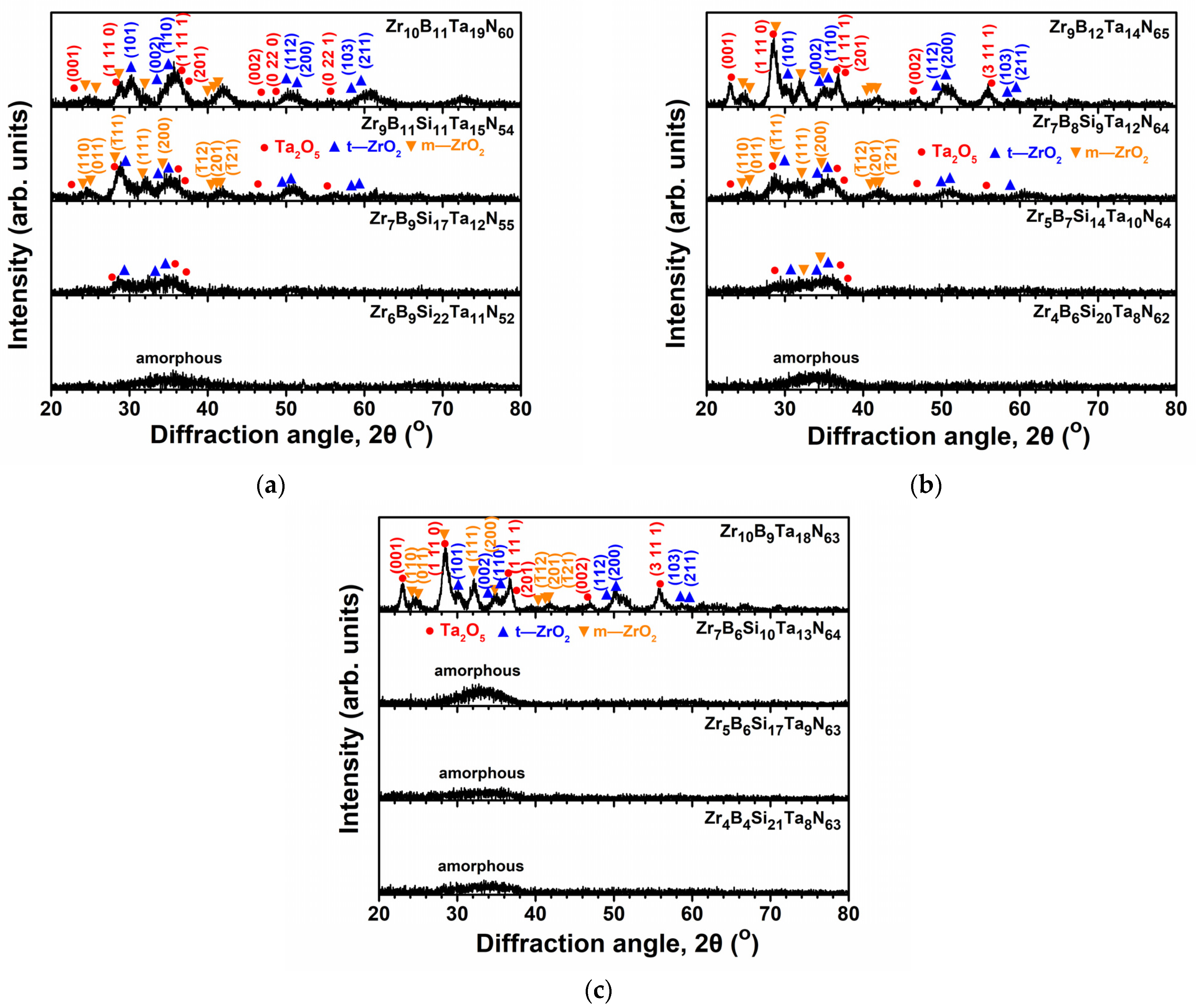
The oxidation and crystallization of the Zr
10B
11Ta
19N
60 (B1) and Zr
9B
11Si
11Ta
15N
54 (B2) films occurred after 10 min annealing at 900 °C. In contrast, crystallization reflections became evident for the Zr
7B
9Si
17Ta
12N
55 (B3) films after 20 min annealing, and the Zr
6B
9Si
22Ta
11N
52 (B4) films maintained an amorphous phase after annealing for up to 30 min, as
Figure 6a shows. The oxide phases of the (ZrBSiTa)N
x films comprised
m-ZrO
2,
t-ZrO
2, and Ta
2O
5. The oxidation and crystallization of the Zr
9B
12Ta
14N
65 (C1) and Zr
7B
8Si
9Ta
12N
64 (C2) films occurred after 10 min annealing at 900 °C. In contrast, crystallization reflections became evident for the Zr
5B
7Si
14Ta
10N
64 (C3) films after 30 min annealing, and the Zr
4B
6Si
20Ta
8N
62 (C4) films maintained an amorphous phase after annealing for up to 30 min. The oxidation and crystallization of the Zr
10B
9Ta
18N
63 (D1) films occurred after 10 min annealing at 900 °C, whereas the Zr
7B
6Si
10Ta
13N
64 (D2), Zr
5B
6Si
17Ta
9N
63 (D3), and Zr
4B
4Si
21Ta
8N
63 (D4) films maintained an amorphous phase after annealing for up to 30 min.
Figure 6b,c display the GIXRD patterns of the 900 °C and 30 min annealed batches C and D samples, respectively.
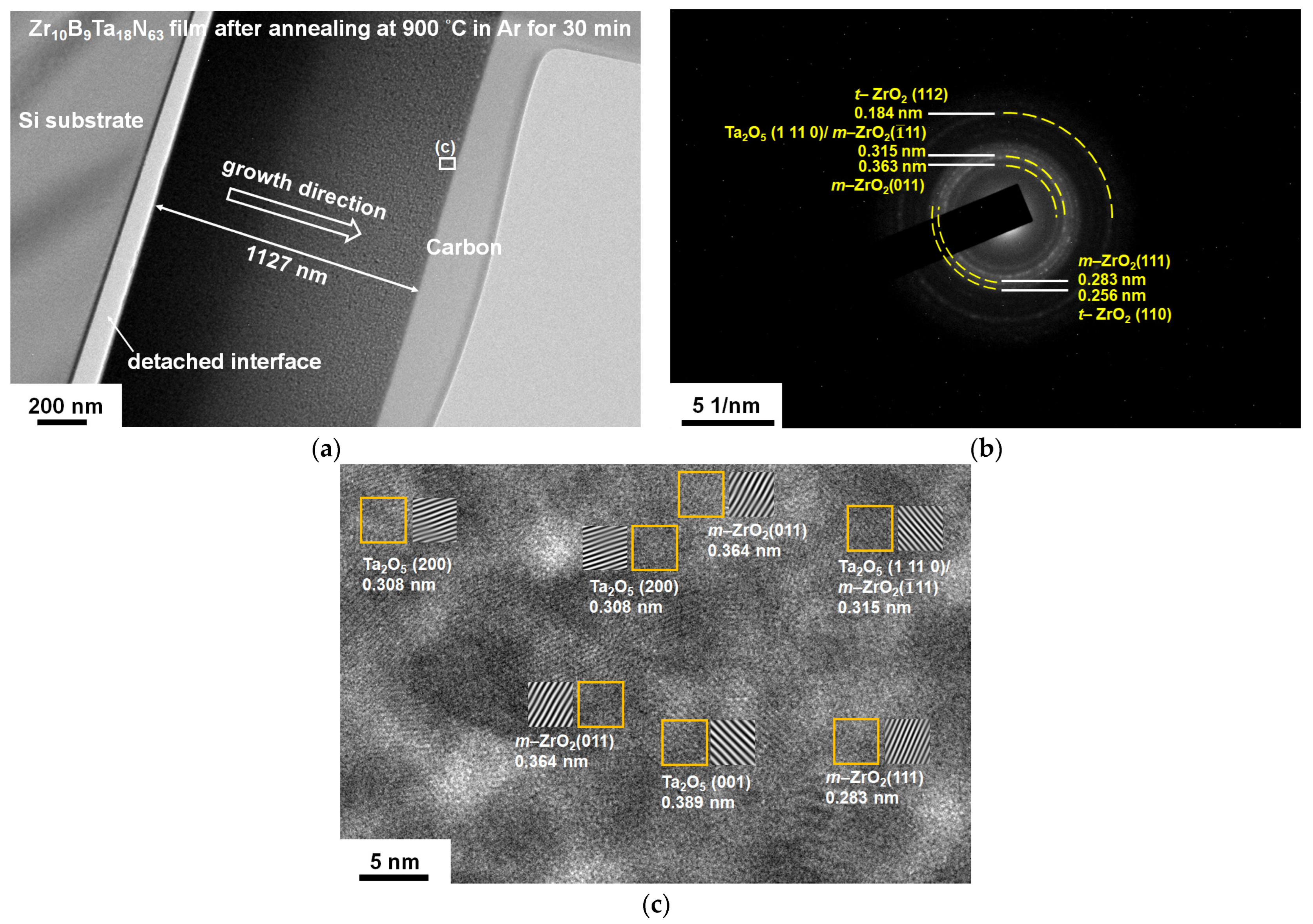
Figure 7a shows a cross-sectional TEM (XTEM) image of the Zr
10B
9Ta
18N
63 (D1) film after 30 min annealing at 900 °C in Ar. The Zr
10B
9Ta
18N
63 film detached from the Si substrate after annealing. The original Zr
10B
9Ta
18N
63 film/Si substrate interface exposed the underlying carbon film on the TEM sample holder.
Figure 7b displays the selected area electron diffraction (SAED) pattern of the annealed Zr
10B
9Ta
18N
63 sample revealing ring patterns of the Ta
2O
5,
m-ZrO
2, and
t-ZrO
2 phases.
Figure 7c displays a high-resolution TEM (HRTEM) image of the annealed Zr
10B
9Ta
18N
63 film, which depicts lattice fringes correlating to
d-spacing values of 0.308, 0.389, 0.364, and 0.283 nm for Ta
2O
5 (200), Ta
2O
5 (001),
m-ZrO
2 (011), and
m-ZrO
2 (111) planes, respectively. The lattice fringes with a
d-spacing of 0.315 nm could represent either Ta
2O
5 (1 11 0) or
m-ZrO
2 (−111) planes.
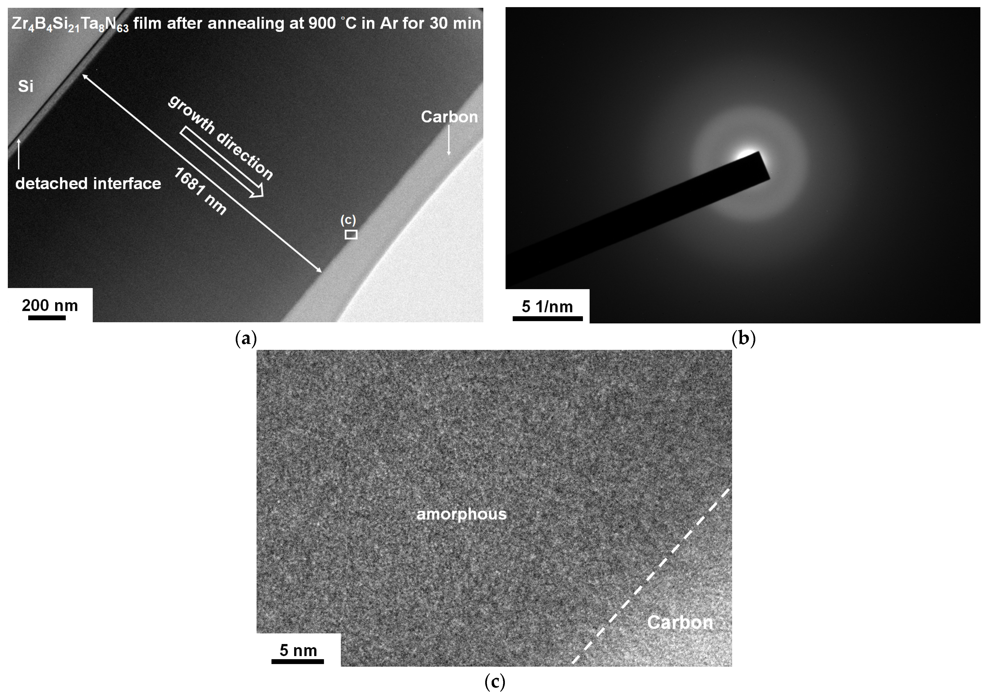
Figure 8a shows the XTEM image of the Zr
4B
4Si
21Ta
8N
63 (D4) film after 30 min annealing at 900 °C in Ar. The Zr
4B
4Si
21Ta
8N
63 film was detached from the Si substrate.
Figure 8b shows an amorphous SAED pattern. The HRTEM image observes no crystalline lattice fringes (
Figure 8c). The Zr
4B
4Si
21Ta
8N
63 film maintained an amorphous phase for up to 30 min as annealed at 900 °C.
3.4. Oxidation Behavior of (ZrBSiTa)Nx Films
The (ZrBSiTa)N
x samples were annealed at 800 °C in air for 0.5, 1, 2, and 12 h.
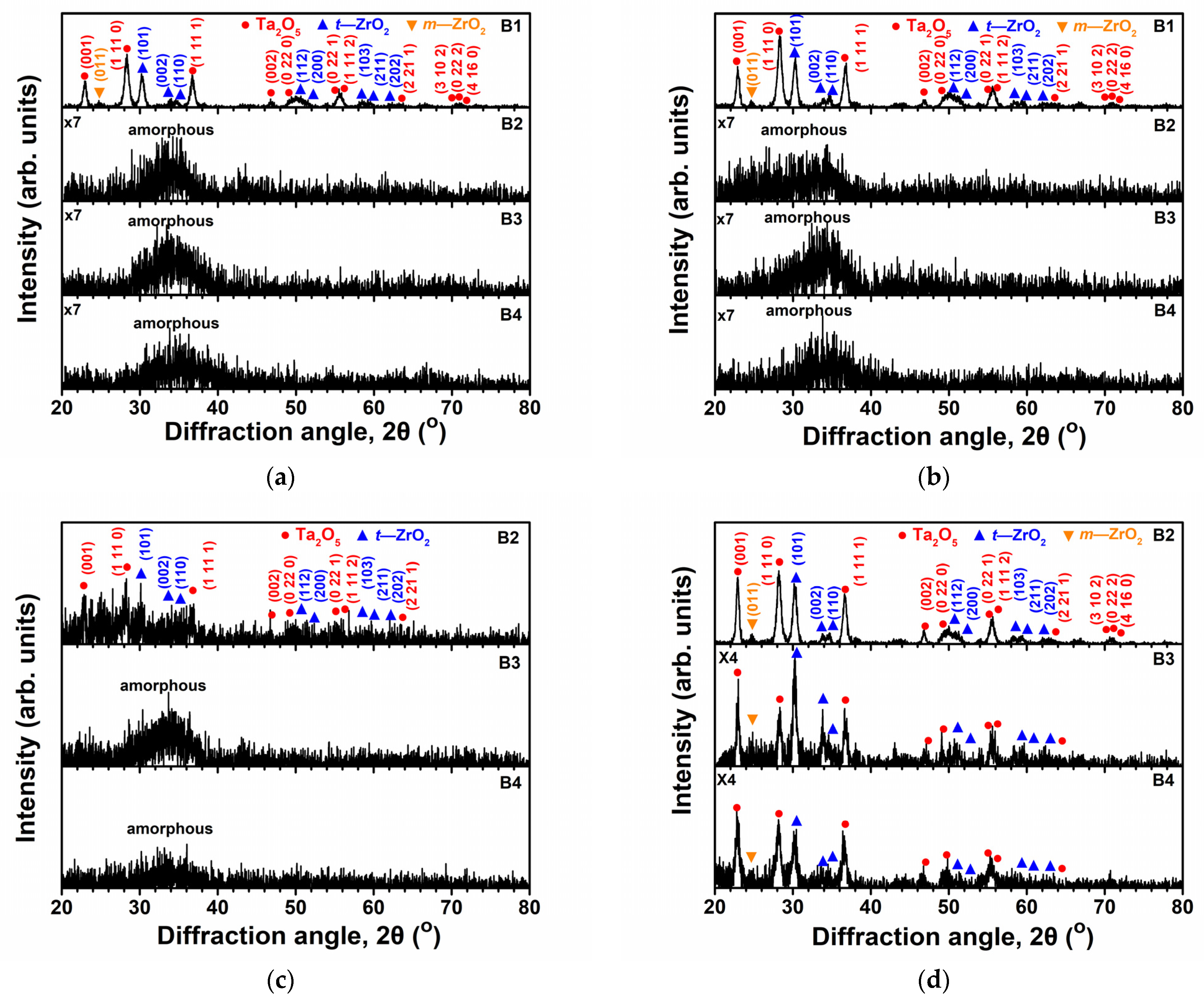
Figure 9 shows the GIXRD patterns of the batch B films after annealing at 800 °C in air. The
t-ZrO
2,
m-ZrO
2, and Ta
2O
5 phases formed for the annealed Zr
10B
11Ta
19N
60 (B1) sample, whereas the Zr
9B
11Si
11Ta
15N
54 (B2), Zr
7B
9Si
17Ta
12N
55 (B3), and Zr
6B
9Si
22Ta
11N
52 (B4) samples maintained an amorphous phase after annealing for 0.5 h. The one h annealed samples revealed XRD patterns similar to those of the 0.5 h annealed samples. After 2 h annealing, the Zr
9B
11Si
11Ta
15N
54 sample crystallized, and the Zr
7B
9Si
17Ta
12N
55 and Zr
6B
9Si
22Ta
11N
52 samples maintained an amorphous phase. The Zr
7B
9Si
17Ta
12N
55 and Zr
6B
9Si
22Ta
11N
52 samples crystallized after 12 h annealing. The oxidation behavior of batches C and D samples was similar to those of the batch B samples. The Si content affected the oxidation resistance of (ZrBSiTa)N
x films. The B1, C1, and D1 samples without Si content oxidized after 0.5 h annealing at 800 °C, whereas the B2, C2, and D2 samples with Si contents of 9–11 at.% oxidized after 2 h annealing. The B3, C3, D3, B4, C4, and D4 samples with Si contents of 14–22 at.% maintained an amorphous phase after 2 h annealing. In this study, B and Si in the (ZrBSiTa)N
x films stabilized the amorphous phase. However, the oxidation resistance of (ZrBSiTa)N
x films was determined by the amorphous Si
3N
4 content, which was comparable with the oxidation behavior of ZrSiN films with a high Si content (≥25 at.%) [
16].
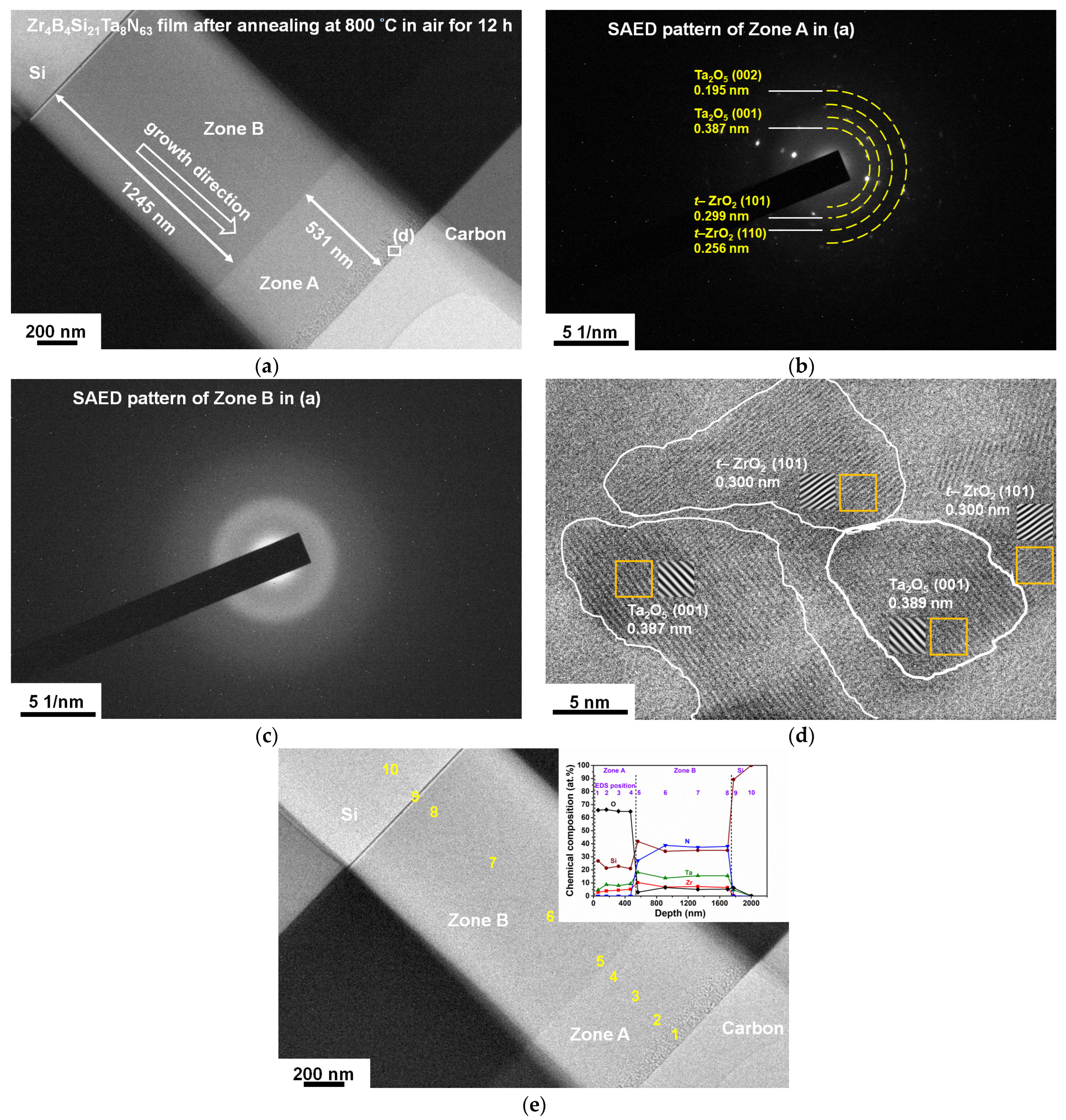
Figure 10a depicts an XTEM image of the Zr
4B
4Si
21Ta
8N
63 (D4) film after 12 h annealing at 800 °C in the air. An oxide scale of 531 nm (zone A) was observed, and the SAED pattern (
Figure 10b) indicated that this scale was crystalline and consisted of
t-ZrO
2 and Ta
2O
5 phases. Beneath the oxide scale, zone B of the annealed Zr
4B
4Si
21Ta
8N
63 film exhibited a dense structure, and its SAED pattern showed an amorphous phase (
Figure 10c).
Figure 10d shows an HRTEM image of the surface oxide scale, and lattice fringes identified for tetragonal ZrO
2 (101) and orthorhombic Ta
2O
5 (001) planes are indicated.
Figure 10e depicts the EDS analysis of the annealed Zr
4B
4Si
21Ta
8N
63 film, which suggests that the Zr
4B
4Si
21Ta
8N
63 film is partially oxidized. Zone A was oxide-dominant, and zone B was amorphous nitride-dominant after 12 h annealing at 800 °C in the air.
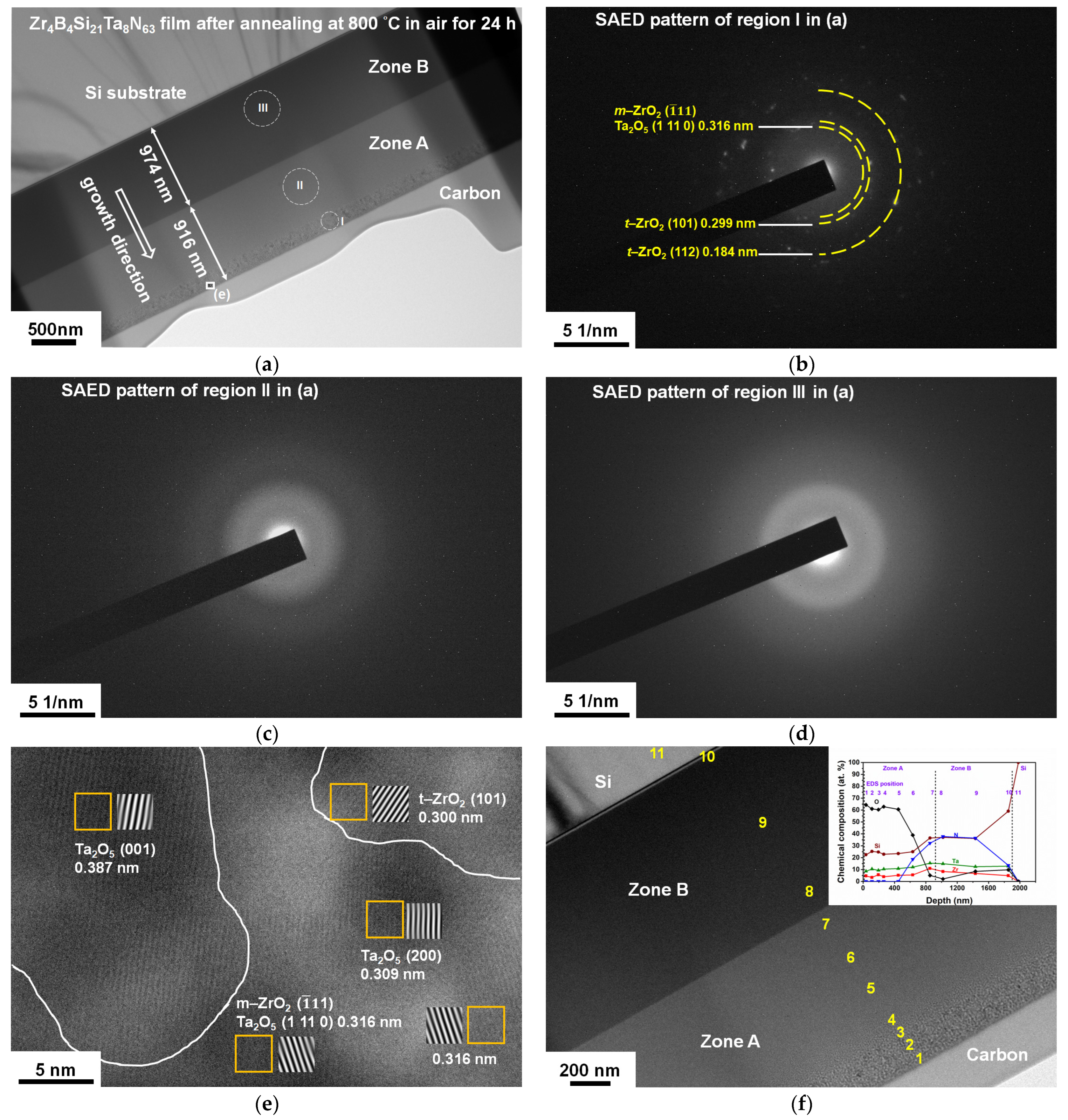
Figure 11a displays an XTEM image of the Zr
4B
4Si
21Ta
8N
63 film after 24 h annealing at 800 °C in the air. The oxide scale (zone A) expanded relative to that of the 12 h annealed Zr
4B
4Si
21Ta
8N
63 film. The SAED patterns of regions I, II, and III indicated in
Figure 11a are shown in
Figure 11b–d, respectively. Region I, the outermost part of the oxide scale, exhibits diffraction rings of
m-ZrO
2,
t-ZrO
2, and Ta
2O
5 phases. In contrast, the inner part of the oxide scale (Region II) and the unoxidized film (Region III) are amorphous.
Figure 11e shows an HRTEM image of region I displaying crystalline lattice fringes.
Figure 11f displays the EDS analysis results of the 24 h annealed Zr
4B
4Si
21Ta
8N
63 sample.


