
Characterization of ZrBSiTaNx Films


Abstract
1. Introduction
2. Materials and Methods
3. Results
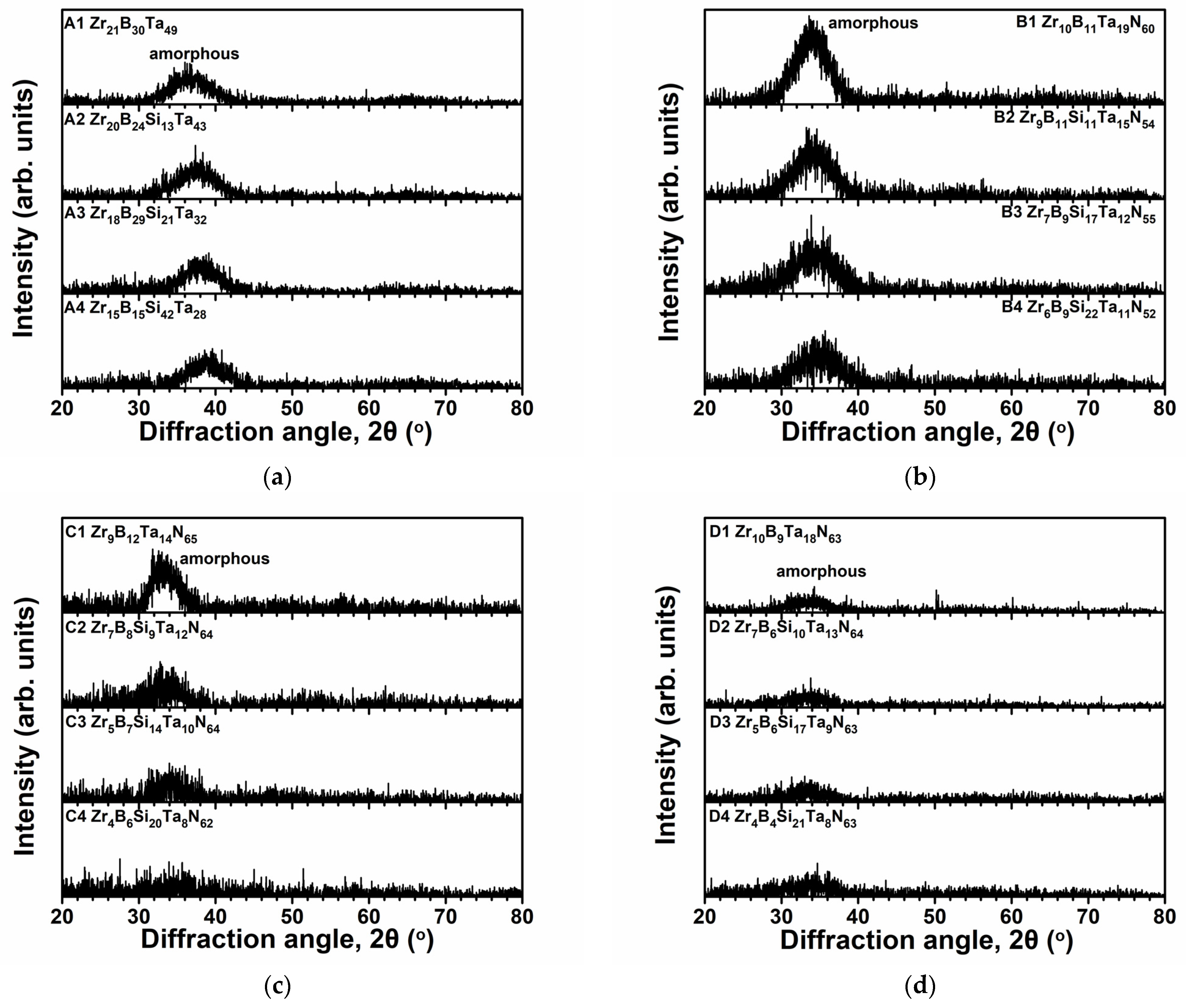
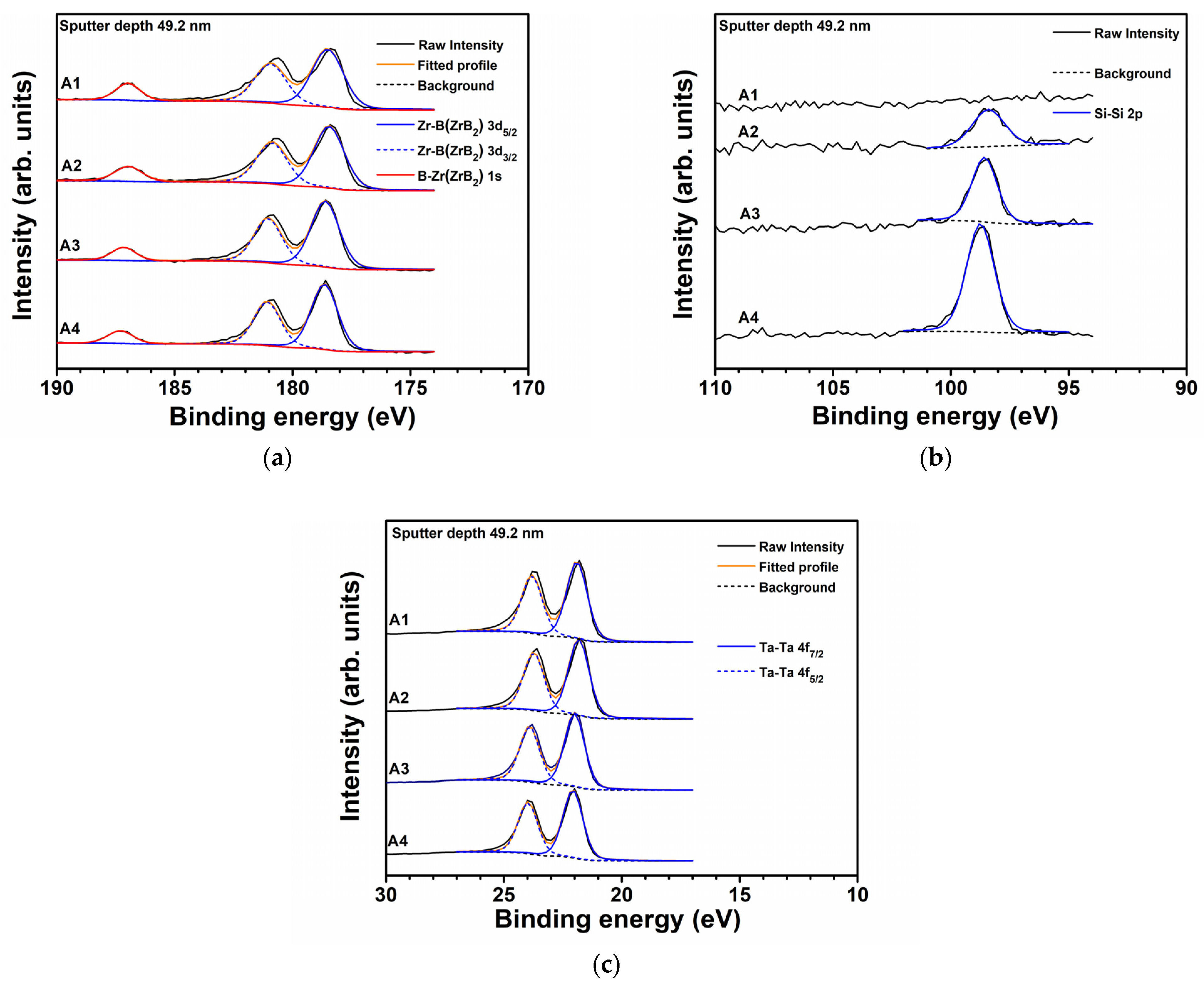
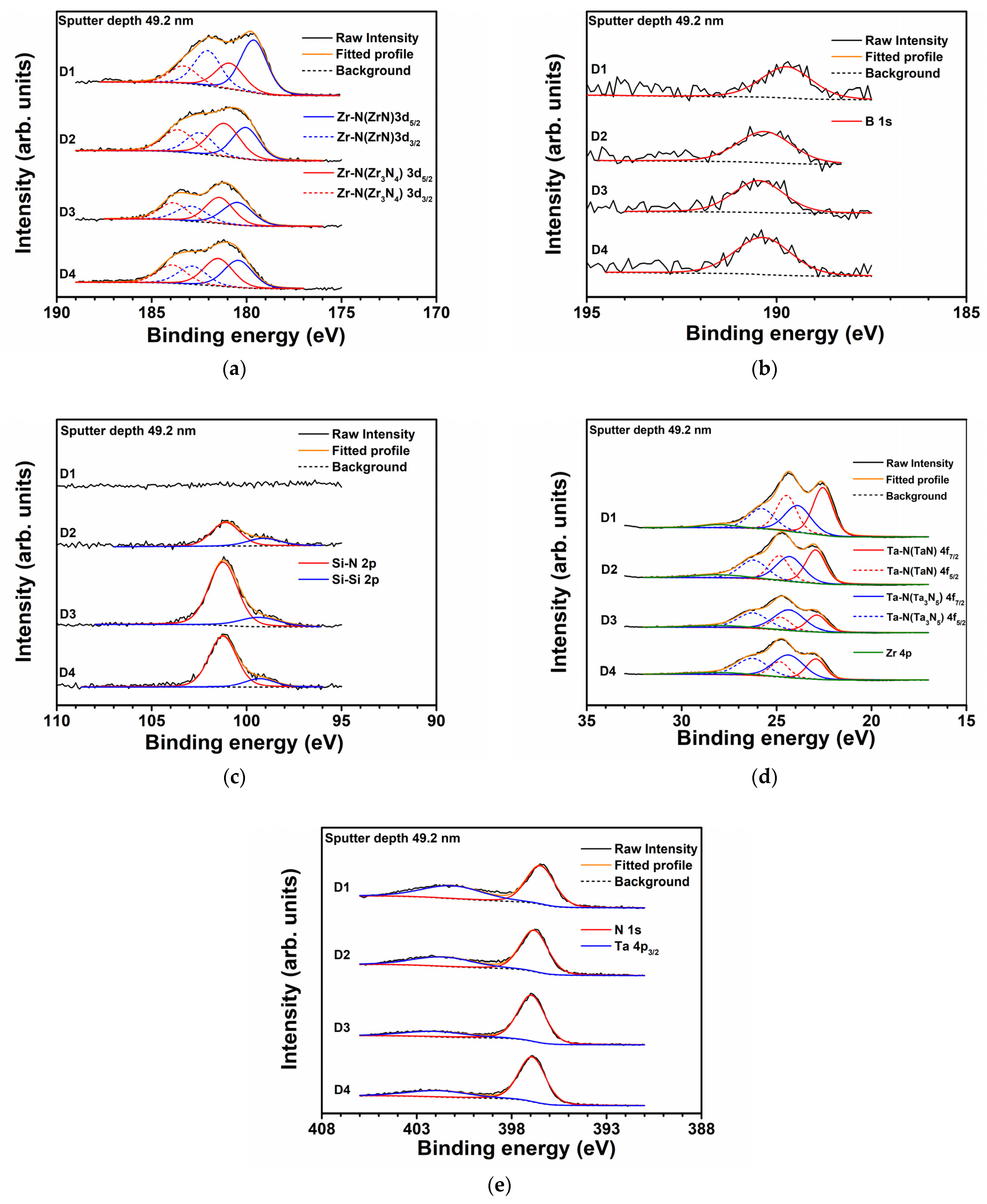
3.1. Chemical Compositions and Phase Structures of ZrBSiTa and (ZrBSiTa)Nx Films
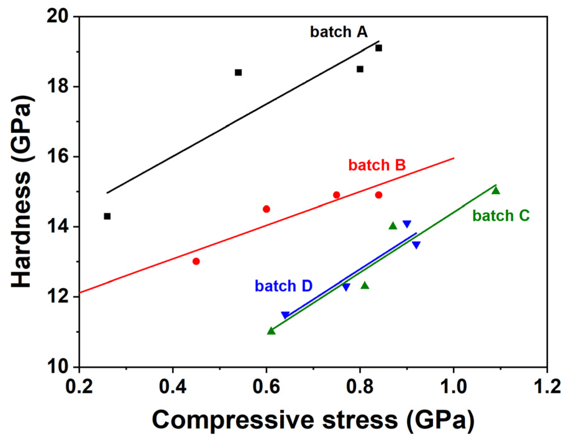
3.2. Mechanical Properties
3.3. Thermal Stability of ZrBSiTa and ZrBSiTaN Films
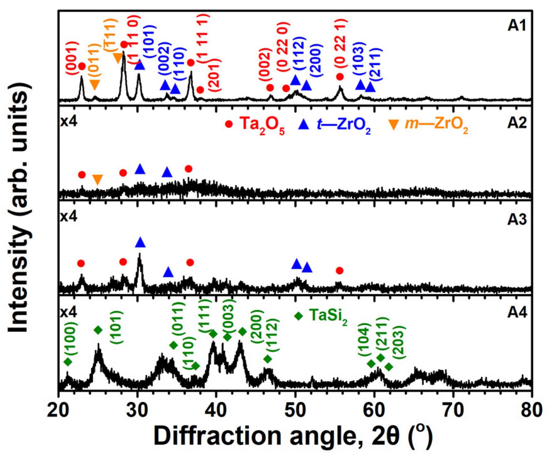
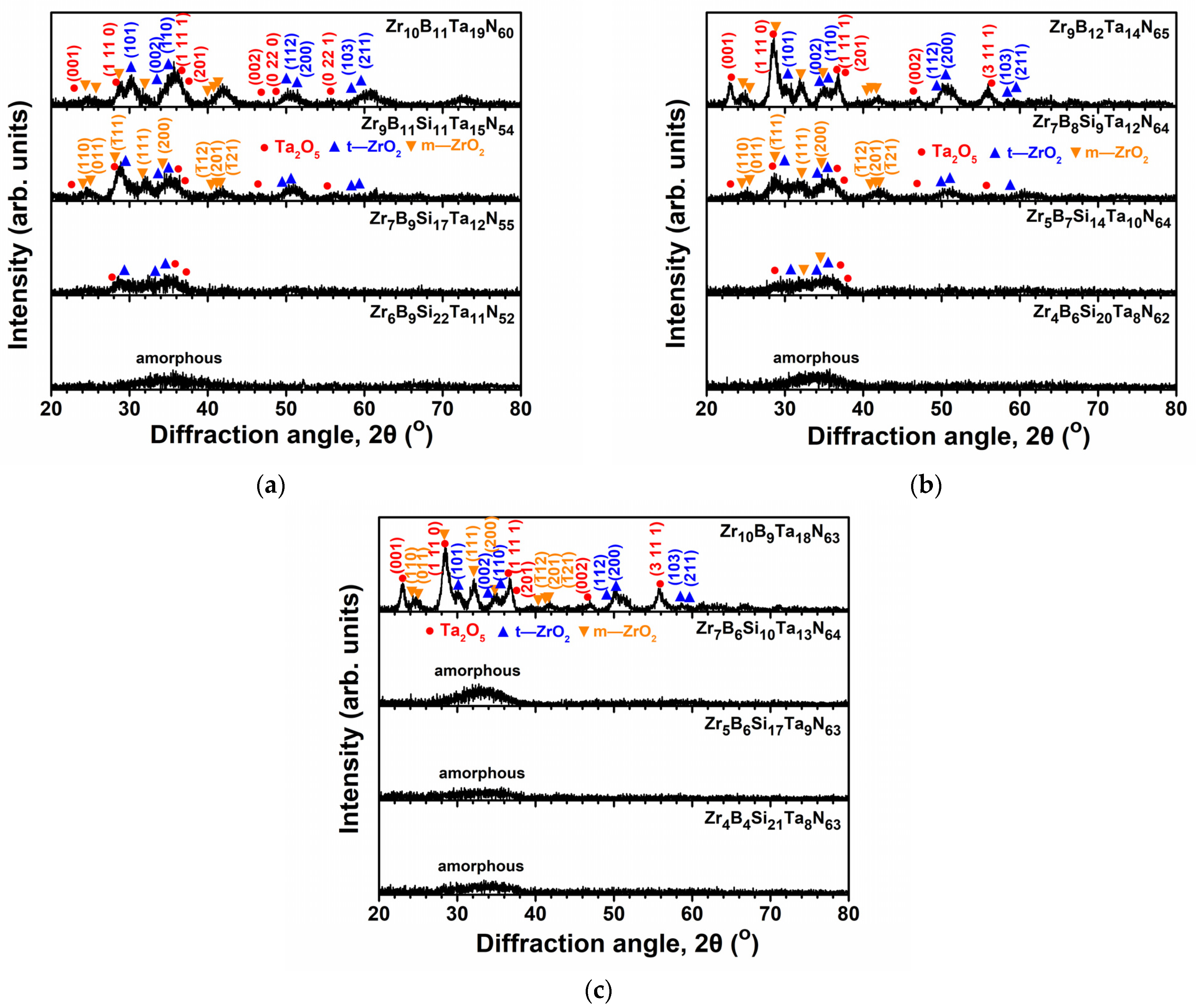
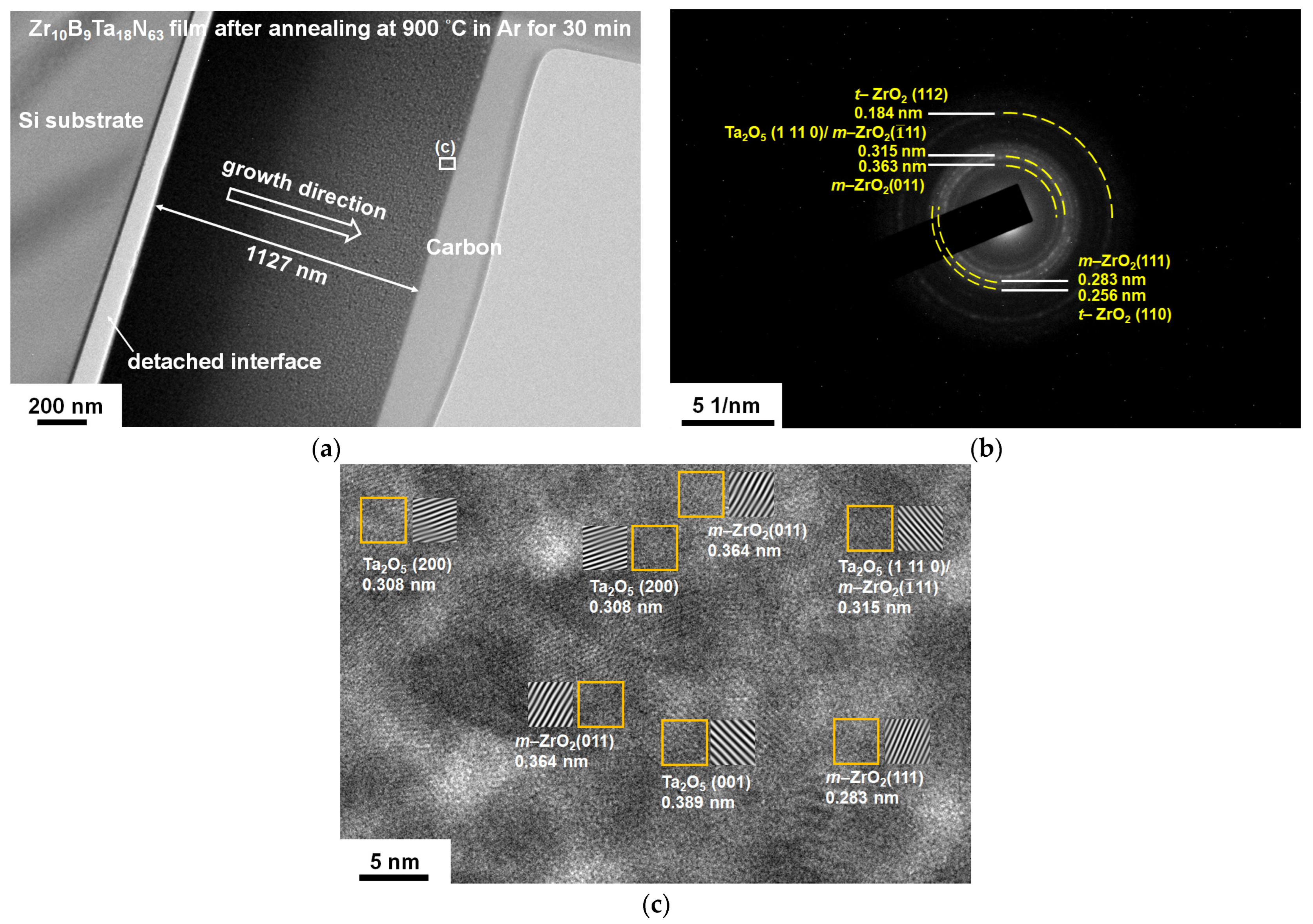
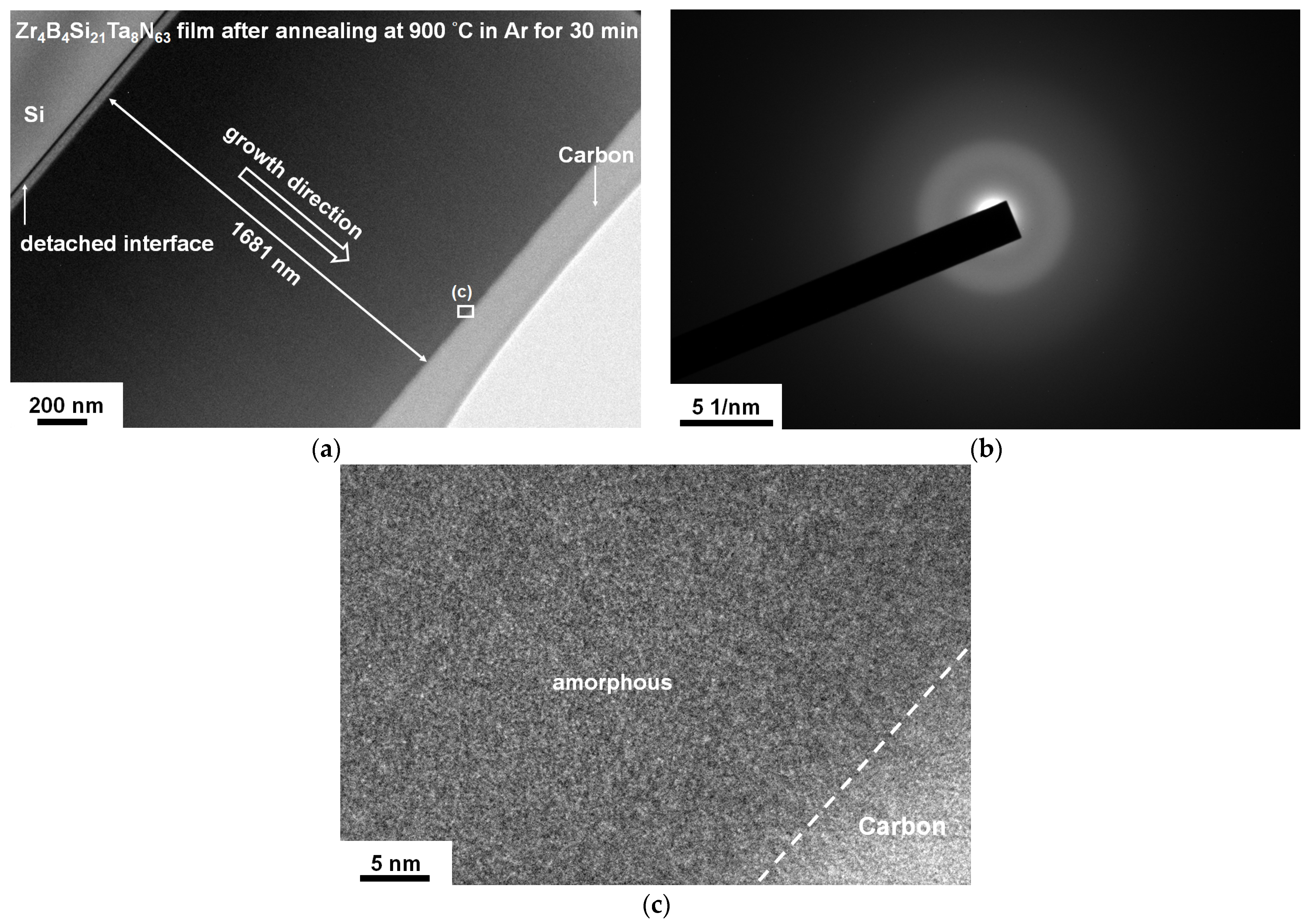
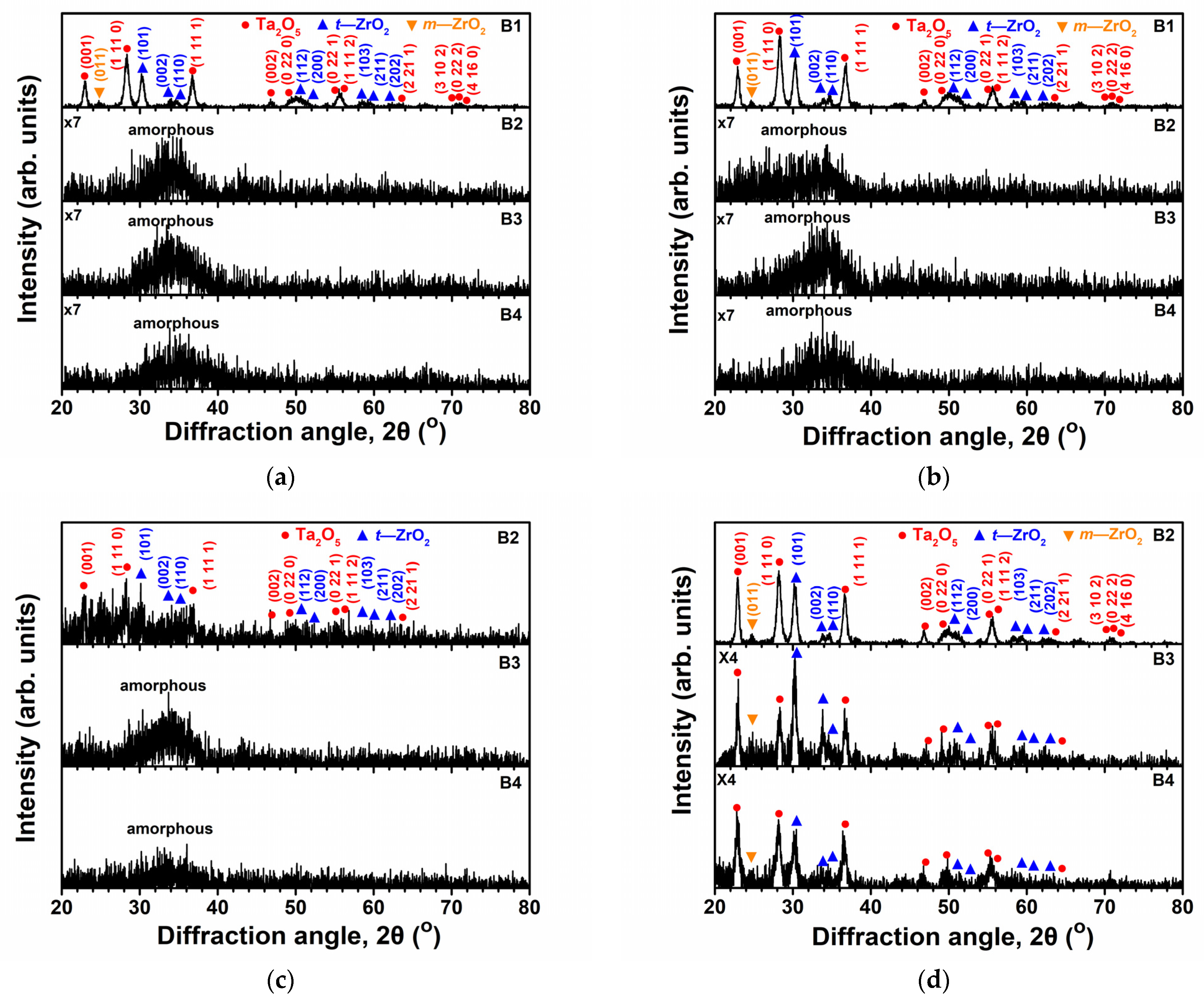
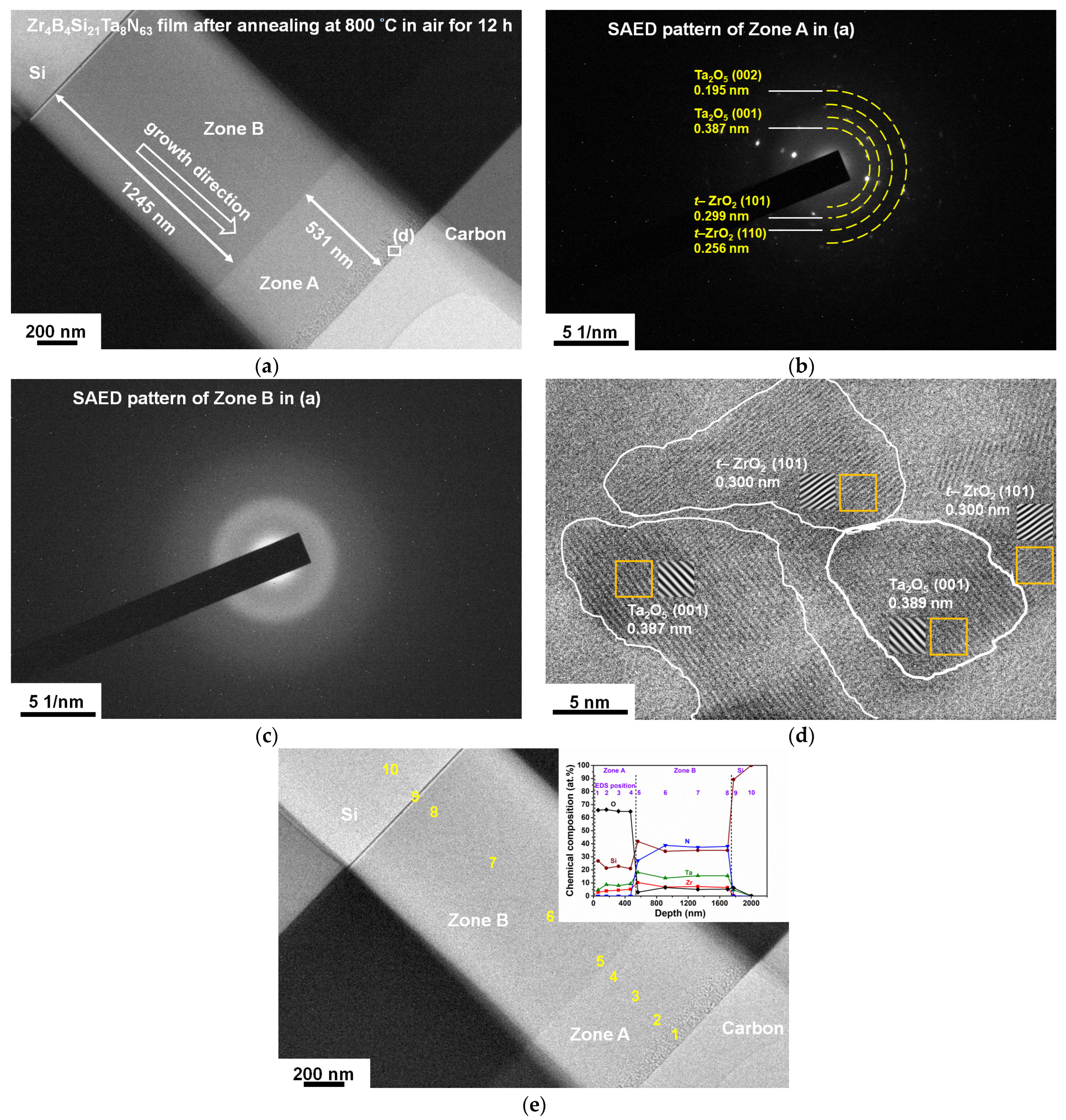
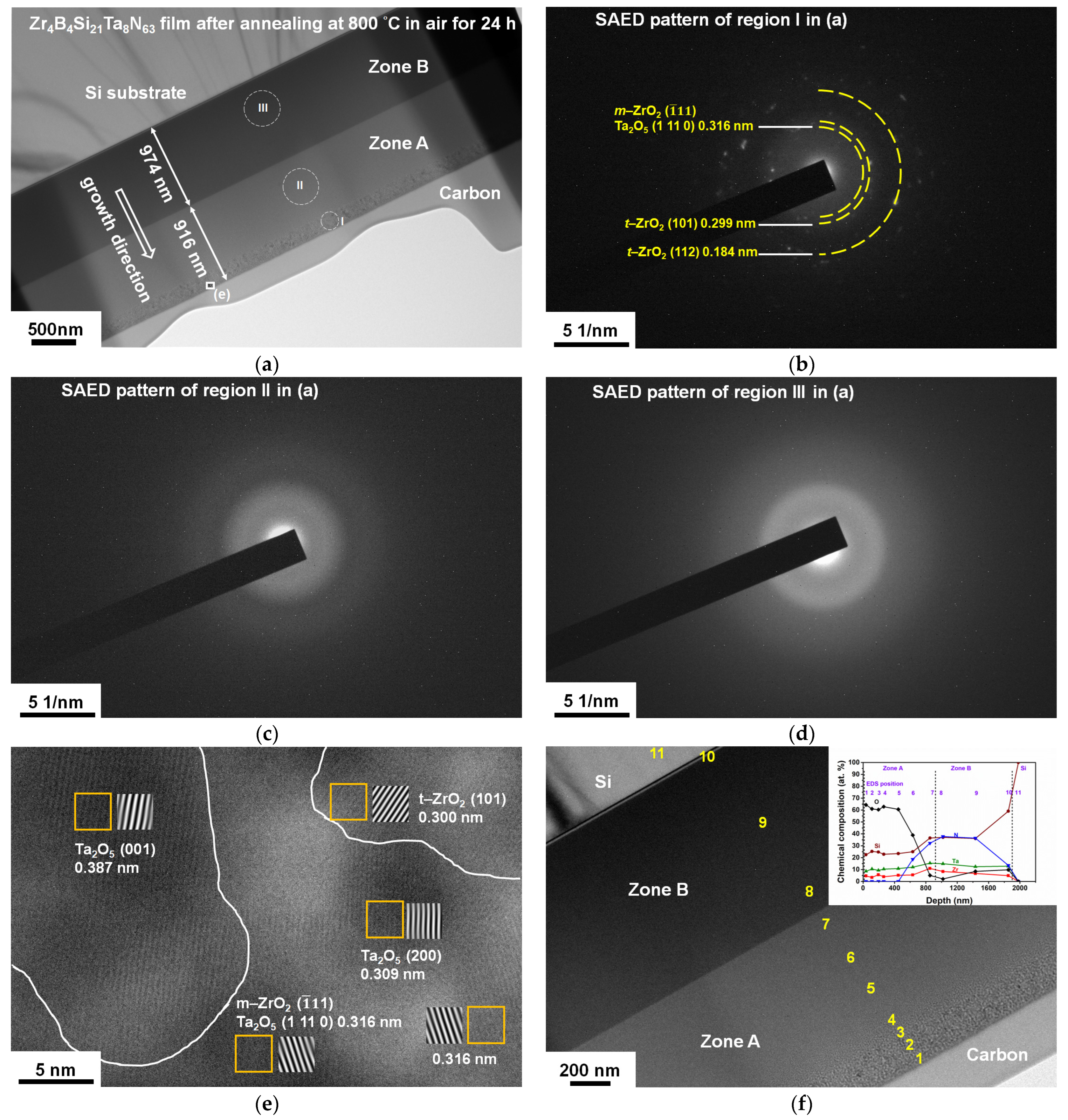
3.4. Oxidation Behavior of (ZrBSiTa)Nx Films
4. Conclusions
- (1)
- All the as-fabricated ZrBSiTa and (ZrBSiTa)Nx films exhibited amorphous structures due to incorporating B and Si. The overstoichiometric ratio (x > 1) was obtained for the (ZrBSiTa)Nx films.
- (2)
- The as-fabricated ZrBSiTa films exhibited hardness values of 14.3–19.1 GPa and Young’s modulus values of 242–264 GPa. The hardness and Young’s modulus values of the (ZrBSiTa)Nx thin films decreased to 11.0–15.0 and 181–223 GPa, respectively.
- (3)
- The amorphous (ZrBSiTa)Nx films with high Si contents exhibited high thermal stability when annealed at 800 and 900 °C for up to 30 min in an Ar-purged atmosphere.
- (4)
- The Si content dominated the oxidation resistance of (ZrBSiTa)Nx films. The (ZrBSiTa)Nx films with Si contents of 14–22 at.% maintained an amorphous phase after 2 h annealing at 800 °C in air. The lower part of the Zr4B4Si21Ta8N63 film held amorphous nitride after extending the annealing time to 24 h.
Author Contributions
Funding
Institutional Review Board Statement
Informed Consent Statement
Data Availability Statement
Acknowledgments
Conflicts of Interest
References
- Chen, H.W.; Chan, Y.C.; Lee, J.W.; Duh, J.G. Oxidation resistance of nanocomposite CrAlSiN under long-time heat treatment. Surf. Coat. Technol. 2011, 206, 1571–1576. [Google Scholar] [CrossRef]
- Dong, Y.; Zhu, H.; Ge, F.; Zhao, G.; Huang, F. Microstructural effects on the high-temperature steam oxidation resistance of magnetron sputtered Cr-Al-Si-N quaternary coatings on zirconium coupons. Surf. Coat. Technol. 2019, 374, 393–401. [Google Scholar] [CrossRef]
- Tzeng, C.H.; Chang, L.C.; Chen, Y.I. Mechanical Properties and Oxidation Behavior of TaWSiN Films. Materials 2022, 15, 8179. [Google Scholar] [CrossRef] [PubMed]
- Chang, L.C.; Sung, M.C.; Chen, Y.I.; Tseng, C.H. Mechanical properties and oxidation behavior of CrWSiN films. Surf. Coat. Technol. 2022, 437, 128368. [Google Scholar] [CrossRef]
- Mejía, V.C.P.; Chellali, M.R.; Garzón, C.M.; Olaya, J.J.; Hahn, H.; Velasco, L. Effect of discharge current on the corrosion resistance and microstructure of ZrTiSiN coatings deposited by magnetron co-sputtering. Mater. Today Commun. 2021, 26, 102151. [Google Scholar] [CrossRef]
- Li, C.L.; Chung, C.Y.; Lou, B.S.; Lee, J.W.; Chu, J.P. Effect of nitrogen content on the corrosion resistance of Zr-Ni-Al-Si thin film metallic glass. Int. J. Electrochem. Sci. 2017, 12, 12074–12083. [Google Scholar] [CrossRef]
- Tang, Q.L.; Wu, Y.C.; Lou, B.S.; Chen, Z.Y.; Lee, J.W. Mechanical property evaluation of ZrSiN films deposited by a hybrid superimposed high power impulse- medium frequency sputtering and RF sputtering system. Surf. Coat. Technol. 2019, 376, 59–67. [Google Scholar] [CrossRef]
- Hsueh, H.T.; Shen, W.J.; Tsai, M.H.; Yeh, J.W. Effect of nitrogen content and substrate bias on mechanical and corrosion properties of high-entropy films (AlCrSiTiZr)100−xNx. Surf. Coat. Technol. 2012, 206, 4106–4112. [Google Scholar] [CrossRef]
- Fréty, N.; Bernard, F.; Nazon, J.; Sarradin, J.; Tedenac, J.C. Copper diffusion Into silicon substrates through TaN and Ta/TaN multilayer barriers. J. Phase Equilibria Diffus. 2006, 27, 590–597. [Google Scholar] [CrossRef]
- Cabral, C., Jr.; Saenger, K.L.; Kotecki, D.E.; Harper, J.M.E. Optimization of Ta–Si–N thin films for use as oxidation-resistant diffusion barriers. J. Mater. Res. 2000, 15, 194–198. [Google Scholar] [CrossRef]
- Musil, J. Hard nanocomposite coatings: Thermal stability, oxidation resistance and toughness. Surf. Coat. Technol. 2012, 207, 50–65. [Google Scholar] [CrossRef]
- Reid, J.S.; Kolawa, E.; Garland, C.M.; Nicolet, M.A.; Cardone, F.; Gupta, D.; Ruiz, R.P. Amorphous (Mo, Ta, or W)–Si–N diffusion barriers for Al metallizations. J. Appl. Phys. 1996, 79, 1109–1115. [Google Scholar] [CrossRef]
- Sun, X.; Reid, J.S.; Kolawa, E.; Nicolet, M.A.; Ruiz, R.P. Reactively sputtered Ti-Si-N films. II. Diffusion barriers for Al and Cu metallizations on Si. J. Appl. Phys. 1997, 81, 664–671. [Google Scholar] [CrossRef]
- Chen, Y.I.; Yeh, K.H.; Ou, T.Y.; Chang, L.C. Diffusion barrier characteristics of WSiN films. Coatings 2022, 12, 811. [Google Scholar] [CrossRef]
- Daniel, R.; Musil, J.; Zeman, P.; Mitterer, C. Thermal stability of magnetron sputtered Zr–Si–N films. Surf. Coat. Technol. 2006, 201, 3368–3376. [Google Scholar] [CrossRef]
- Musil, J.; Daniel, R.; Zeman, P.; Takai, O. Structure and properties of magnetron sputtered ZrSiN films with a high (≥25 at.%) Si content. Thin Solid Films 2005, 478, 238–247. [Google Scholar] [CrossRef]
- Musil, J.; Zeman, P.; Dohnal, P. Ti-Si-N films with a high content of Si. Plasma Process. Polym. 2007, 4, 574–578. [Google Scholar] [CrossRef]
- Mikula, M.; Grančič, B.; Drienovský, M.; Satrapinskyy, L.; Roch, T.; Hájovská, Z.; Gregor, M.; Plecenik, T.; Čička, R.; Plecnik, A.; et al. Thermal stability and high temperature oxidation behavior of Si–Cr–N coatings with high content of silicon. Surf. Coat. Technol. 2013, 232, 349–356. [Google Scholar] [CrossRef]
- Veprek, S.; Veprek-Heijman, M.G.J.; Karvankova, P.; Prochazka, J. Different approaches to superhard coatings and nanocomposites. Thin Solid Films 2005, 476, 1–29. [Google Scholar] [CrossRef]
- Mayrhofer, P.H.; Mitterer, C.; Hultman, L.; Clemens, H. Microstructural design of hard coatings. Prog. Mater. Sci. 2006, 51, 1032–1114. [Google Scholar] [CrossRef]
- Budna, K.P.; Mayrhofer, P.H.; Neidhardt, J.; Hegedũs, É.; Kovács, I.; Tóth, L.; Pécz, B.; Mitterer, C. Effect of nitrogen-incorporation on structure, properties and performance of magnetron sputtered CrB2. Surf. Coat. Technol. 2008, 202, 3088–3093. [Google Scholar] [CrossRef]
- Gu, Q.; Krauss, G.; Steurer, W. Transition metal borides: Superhard versus Ultra-incompressible. Adv. Mater. 2008, 20, 3620–3626. [Google Scholar] [CrossRef]
- Goncharov, A.A.; Dub, S.N.; Agulov, A.V.; Petukhov, V.V. Structure, composition, and mechanical properties of thin films of transition metals diborides. J. Superhard Mater. 2015, 37, 422–428. [Google Scholar] [CrossRef]
- Bazhin, A.I.; Goncharov, A.A.; Pogrebnyak, A.D.; Stupak, V.A.; Goncharova, S.A. Superhardness effect in transition-metal diborides films. Phys. Met. Metallogr. 2016, 117, 594. [Google Scholar] [CrossRef]
- Moraes, V.; Riedl, H.; Fuger, C.; Polcik, P.; Bolvardi, H.; Holec, D.; Mayrhofer, P.H. Ab initio inspired design of ternary boride thin films. Sci. Rep. 2018, 8, 9288. [Google Scholar] [CrossRef] [PubMed]
- Bakhit, B.; Engberg, D.L.J.; Lu, J.; Rosen, J.; Högberg, H.; Hultman, L.; Petrov, I.; Greene, J.E.; Greczynski, G. Strategy for simultaneously increasing both hardness and toughness in ZrB2-rich Zr1−xTaxBy thin films. J. Vac. Sci. Technol. A 2019, 37, 031506. [Google Scholar] [CrossRef]
- Clegg, W.J. Controlling cracks in ceramics. Science 1999, 286, 1097–1099. [Google Scholar] [CrossRef]
- Asempah, I.; Xu, J.; Yu, L.; Ju, H.; Wu, F.; Luo, H. Microstructure, mechanical and tribological properties of magnetron sputtered Ti-B-N films. Surf. Eng. 2019, 35, 701–709. [Google Scholar] [CrossRef]
- Lee, J.W.; Cheng, C.H.; Chen, H.W.; Chan, C.; Duh, J.G.; Ho, L.W. Effects of boron and nitrogen contents on the microstructures and mechanical properties of Cr-B-N nanocomposite thin films. Proc. Eng. 2012, 36, 360–367. [Google Scholar] [CrossRef][Green Version]
- Kiryukhantsev-Korneev, P.V.; Sytchenko, A.D.; Kozlova, N.S.; Zabelina, E.V.; Skryleva, E.A.; Kaplansky, Y.Y.; Vakhrushev, R.A.; Levashov, E.A. Structure and properties of protective amorphous Zr–B–N coating. Surf. Coat. Technol. 2022, 448, 128849. [Google Scholar] [CrossRef]
- Chang, L.C.; Liu, B.W.; Cen, Y.I. Mechanical properties and oxidation behavior of multilayered Hf–Si–N coatings. Coatings 2018, 8, 354. [Google Scholar] [CrossRef]
- Moulder, J.F.; Stickle, W.F.; Sobol, P.E.; Bomben, K.D. Handbook of X-ray Photoelectron Spectroscopy; Chastain, J., King, R.C., Eds.; Physical Electronics: Chanhassen, MN, USA, 1995. [Google Scholar]
- Oliver, W.C.; Pharr, G.M. An improved technique for determining hardness and elastic modulus using load and displacement sensing indentation experiments. J. Mater. Res. 1992, 7, 1564–1583. [Google Scholar] [CrossRef]
- Janssen, G.C.A.M.; Abdalla, M.M.; van Keulen, F.; Pujada, B.R.; van Venrooy, B. Celebrating the 100th anniversary of the Stoney equation for film stress: Developments from polycrystalline steel strips to single crystal silicon wafers. Thin Solid Films 2009, 517, 1858–1867. [Google Scholar] [CrossRef]
- Chang, L.C.; Zheng, Y.Z.; Chen, Y.I.; Chang, S.C.; Liu, B.W. Bonding characteristics and chemical inertness of Zr–Si–N coatings with a high Si content in glass molding. Coatings 2018, 8, 181. [Google Scholar] [CrossRef]
- Lee, J.W.; Chen, C.Y.; Chen, Y.J.; Tzeng, C.H.; Chen, Y.I. Effects of nitrogen flow ratio on the structural, mechanical, and anticorrosive properties of co-sputtered (NbTaMoW)Nxfilms. J. Mater. Res. Technol. 2022, 21, 1890–1902. [Google Scholar] [CrossRef]
- Barin, I. Thermochemical Data of Pure Substances, 3rd ed.; VCH: New York, NY, USA, 1995. [Google Scholar]
- Dorri, S.; Palisaitis, J.; Greczynski, G.; Petrov, I.; Birch, J.; Hultman, L.; Bakhit, B. Oxidation kinetics of overstoichiometric TiB2 thin films grown by DC magnetron sputtering. Corros. Sci. 2022, 206, 110493. [Google Scholar] [CrossRef]
- Chiu, H.S.; Ou, T.Y.; Chen, Y.I. Effects of thickness ratio on phase structures, mechanical properties, and wear behaviors of CrN/ZrB2 bilayer films. Surf. Coat. Technol. 2024, 481, 130694. [Google Scholar] [CrossRef]
- Lou, B.S.; Wang, C.J.; Chen, Y.Y.; Hung, S.B.; Lin, Y.C.; Lee, J.W. Phase, mechanical property and corrosion resistance evaluation of W-Nb-Ta-Ti and W-Nb-Ta-Ti-N medium entropy alloy thin films. Surf. Coat. Technol. 2022, 442, 128339. [Google Scholar] [CrossRef]
- Pogrebnjak, A.D.; Bagdasaryan, A.A.; Yakushchenko, I.V.; Beresnev, V.M. The structure and properties of high-entropy alloys and nitride coatings based on them. Russ. Chem. Rev. 2014, 83, 1027–1061. [Google Scholar] [CrossRef]
- Yang, J.F.; Yuan, Z.G.; Wang, X.P.; Fang, Q.F. Characterization of W–Ta–N hard films synthesized by direct current magnetron sputtering. Surf. Coat. Technol. 2013, 231, 19–23. [Google Scholar] [CrossRef]
- Chang, L.C.; Chang, C.Y.; Chen, Y.I. Mechanical properties and oxidation resistance of reactively sputtered Ta1−xZrxNy thin films. Surf. Coat. Technol. 2015, 280, 27–36. [Google Scholar] [CrossRef]
- Zhang, Y.; Zhou, Y.J.; Lin, J.P.; Chen, G.L.; Liaw, P.K. Solid-solution phase formation rules for multi-component alloys. Adv. Eng. Mater. 2008, 10, 534–538. [Google Scholar] [CrossRef]
- Magnuson, M.; Tengdelius, L.; Greczynski, G.; Hultman, L.; Högberg, H. Chemical bonding in epitaxial ZrB2 studied by X-ray spectroscopy. Thin Solid Films 2018, 649, 89–96. [Google Scholar] [CrossRef]
- Zhu, D.; Shi, M.; Huang, Z.; Qin, Y.; Fu, H.; Deng, Z. Thermal oxidation and compressive failure behavior of ZrSi2–B4C modified phenolic resin-based composite. Polym. Test. 2023, 125, 108128. [Google Scholar] [CrossRef]
- Faussemagne, A.; Delichere, P.; Moncoffre, N.; Benyagoub, A.; Marest, G. Study of BN formation by dual implantation of boron and nitrogen in a 100Cr6 bearing steel. Surf. Coat. Technol. 1996, 83, 70–73. [Google Scholar] [CrossRef]
- Nordberg, R.; Brecht, H.; Albridge, R.G.; Fahlman, A.; Van Wazer, J.R. Binding energy of the “2p” electrons of silicon in various compounds. Inorg. Chem. 1970, 9, 2469–2474. [Google Scholar] [CrossRef]
- Ding, W.; Li, L.; Zhang, L.; Ju, D.; Peng, S.; Chai, W. An XPS study on the chemical bond structure at the interface between SiOxNy and N doped polyethylene terephthalate. J. Chem. Phys. 2013, 138, 104706. [Google Scholar] [CrossRef]
- Li, H.; Li, J.; Yan, C.; Hunag, J.; Wu, Q.; Shi, Y.; Xiong, D. Deposition and mechanical properties of δ-TaNx films with different stoichiometry by DC magnetron sputtering. Surf. Coat. Technol. 2020, 404, 126452. [Google Scholar] [CrossRef]
- Chang, C.C.; Jeng, J.S.; Chen, J.S. Microstructural and electrical characteristics of reactively sputtered Ta-N thin films. Thin Solid Films 2002, 413, 46–51. [Google Scholar] [CrossRef]
- Lin, D.H.; Chnag, K.S. Photocatalytic and photoelectrochemical performance of Ta3N5 microcolumn films fabricated using facile reactive sputtering. J. Appl. Phys. 2016, 120, 075303. [Google Scholar] [CrossRef]


| Sample | Power PSi (W) | RN2 a | Chemical Composition (at.%) | |||||
|---|---|---|---|---|---|---|---|---|
| Zr | B | Si | Ta | N | O | |||
| A1 Zr21B30Ta49 | 0 | 0 | 20.9 ± 0.4 | 29.3 ± 0.3 | – | 48.6 ± 0.7 | – | 1.2 ± 0.9 |
| A2 Zr20B24Si13Ta43 | 50 | 0 | 19.1 ± 0.4 | 24.1 ± 0.4 | 12.9 ± 0.1 | 42.8 ± 0.2 | – | 1.1 ± 0.2 |
| A3 Zr18B29Si21Ta32 | 100 | 0 | 17.7 ± 0.1 | 28.8 ± 0.3 | 20.7 ± 0.2 | 31.0 ± 0.4 | – | 1.8 ± 0.1 |
| A4 Zr15B15Si42Ta28 | 150 | 0 | 14.5 ± 0.1 | 15.0 ± 0.0 | 41.4 ± 0.3 | 26.9 ± 0.4 | – | 2.2 ± 0.1 |
| B1 Zr10B11Ta19N60 | 0 | 0.1 | 10.3 ± 0.2 | 11.3 ± 0.2 | – | 18.7 ± 0.4 | 59.4 ± 0.3 | 0.3 ± 0.5 |
| B2 Zr9B11Si11Ta15N54 | 50 | 0.1 | 8.7 ± 0.1 | 10.9 ± 0.0 | 10.6 ± 0.1 | 14.8 ± 0.3 | 54.5 ± 0.4 | 0.5 ± 0.6 |
| B3 Zr7B9Si17Ta12N55 | 100 | 0.1 | 7.0 ± 0.0 | 8.8 ± 0.3 | 17.4 ± 0.3 | 12.0 ± 0.1 | 54.6 ± 0.5 | 0.2 ± 0.3 |
| B4 Zr6B9Si22Ta11N52 | 150 | 0.1 | 6.4 ± 0.0 | 8.4 ± 0.3 | 22.1 ± 0.4 | 11.3 ± 0.2 | 51.4 ± 0.5 | 0.4 ± 0.1 |
| C1 Zr9B12Ta14N65 | 0 | 0.2 | 8.8 ± 0.1 | 11.9 ± 0.4 | – | 14.3 ± 0.4 | 64.6 ± 0.9 | 0.4 ± 0.4 |
| C2 Zr7B8Si9Ta12N64 | 50 | 0.2 | 6.5 ± 0.1 | 8.0 ± 0.2 | 9.2 ± 0.1 | 12.4 ± 0.1 | 63.4 ± 0.3 | 0.5 ± 0.4 |
| C3 Zr5B7Si14Ta10N64 | 100 | 0.2 | 5.1 ± 0.1 | 6.7 ± 0.1 | 14.3 ± 0.2 | 9.6 ± 0.1 | 64.0 ± 0.2 | 0.3 ± 0.4 |
| C4 Zr4B6Si20Ta8N62 | 150 | 0.2 | 4.4 ± 0.1 | 6.0 ± 0.1 | 19.8 ± 0.1 | 7.5 ± 0.1 | 61.4 ± 0.2 | 0.9 ± 0.1 |
| D1 Zr10B9Ta18N63 | 0 | 0.4 | 9.4 ± 0.1 | 9.1 ± 0.0 | – | 18.2 ± 0.1 | 63.0 ± 0.3 | 0.3 ± 0.4 |
| D2 Zr7B6Si10Ta13N64 | 50 | 0.4 | 6.8 ± 0.0 | 6.2 ± 0.2 | 10.3 ± 0.1 | 13.0 ± 0.2 | 63.5 ± 0.1 | 0.2 ± 0.3 |
| D3 Zr5B6Si17Ta9N63 | 100 | 0.4 | 5.0 ± 0.1 | 5.6 ± 0.1 | 17.1 ± 0.0 | 8.8 ± 0.2 | 63.3 ± 0.1 | 0.2 ± 0.3 |
| D4 Zr4B4Si21Ta8N63 | 150 | 0.4 | 4.2 ± 0.1 | 4.1 ± 0.2 | 20.7 ± 0.1 | 7.5 ± 0.1 | 63.2 ± 0.2 | 0.3 ± 0.1 |
| Sample | Thickness (nm) | Deposition Time (min) | Deposition Rate (nm/min) |
|---|---|---|---|
| A1 | 815 | 120 | 6.8 |
| A2 | 1073 | 120 | 8.9 |
| A3 | 983 | 100 | 9.8 |
| A4 | 881 | 80 | 11.0 |
| B1 | 1608 | 150 | 10.7 |
| B2 | 1530 | 120 | 12.8 |
| B3 | 1684 | 120 | 14.0 |
| B4 | 1536 | 90 | 17.1 |
| C1 | 1189 | 180 | 6.6 |
| C2 | 1593 | 180 | 8.8 |
| C3 | 1377 | 120 | 11.5 |
| C4 | 1547 | 120 | 12.9 |
| D1 | 749 | 160 | 4.7 |
| D2 | 1029 | 180 | 5.7 |
| D3 | 1167 | 170 | 6.9 |
| D4 | 1211 | 150 | 8.1 |
| Sample | Zr 3d5/2 (eV) | B 1s (eV) | Si 2p (eV) | Ta 4f7/2 (eV) |
|---|---|---|---|---|
| A1 | 178.52 ± 0.01 | 187.02 ± 0.02 | — | 21.93 ± 0.02 |
| A2 | 178.49 ± 0.04 | 187.01 ± 0.04 | 98.43 ± 0.02 | 21.88 ± 0.04 |
| A3 | 178.68 ± 0.07 | 187.23 ± 0.06 | 98.75 ± 0.16 | 22.03 ± 0.04 |
| A4 | 178.70 ± 0.06 | 187.33 ± 0.03 | 98.77 ± 0.06 | 22.08 ± 0.02 |
| Sample | Zr 3d5/2 (eV) | B 1s (eV) | Si 2p (eV) | Ta 4f7/2 (eV) | |||
|---|---|---|---|---|---|---|---|
| (ZrN) | (Zr3N4) | (Si) | (Si3N4) | (TaN) | (Ta3N5) | ||
| D1 | 179.60 ± 0.02 | 180.84 ± 0.03 | 189.74 ± 0.04 | — | — | 22.56 ± 0.02 | 23.89 ± 0.03 |
| D2 | 180.06 ± 0.02 | 181.12 ± 0.02 | 190.26 ± 0.04 | 99.02 ± 0.05 | 101.15 ± 0.05 | 22.95 ± 0.02 | 24.34 ± 0.03 |
| D3 | 180.52 ± 0.05 | 181.46 ± 0.03 | 190.44 ± 0.04 | 99.34 ± 0.05 | 101.28 ± 0.05 | 22.91 ± 0.04 | 24.35 ± 0.01 |
| D4 | 180.42 ± 0.02 | 181.46 ± 0.02 | 190.42 ± 0.06 | 99.25 ± 0.07 | 101.28 ± 0.05 | 22.95 ± 0.03 | 24.38 ± 0.02 |
| Sample | H a (GPa) | E b (GPa) | H/E | H3/E2 (GPa) | We c (%) | σ d (GPa) |
|---|---|---|---|---|---|---|
| A1 | 18.5 ± 0.2 | 256 ± 3 | 0.072 | 0.096 | 32 | −0.80 ± 0.15 |
| A2 | 19.1 ± 0.3 | 264 ± 7 | 0.072 | 0.099 | 34 | −0.84 ± 0.01 |
| A3 | 18.4 ± 0.3 | 261 ± 4 | 0.071 | 0.092 | 31 | −0.54 ± 0.08 |
| A4 | 14.3 ± 0.2 | 242 ± 5 | 0.059 | 0.050 | 18 | −0.26 ± 0.05 |
| B1 | 13.0 ± 0.1 | 215 ± 6 | 0.061 | 0.048 | 44 | −0.45 ± 0.05 |
| B2 | 14.5 ± 0.2 | 221 ± 5 | 0.066 | 0.063 | 47 | –0.60 ± 0.03 |
| B3 | 14.9 ± 0.1 | 223 ± 2 | 0.067 | 0.067 | 49 | −0.75 ± 0.23 |
| B4 | 14.9 ± 0.3 | 221 ± 4 | 0.067 | 0.068 | 52 | −0.84 ± 0.05 |
| C1 | 11.0 ± 0.1 | 181 ± 5 | 0.061 | 0.041 | 43 | −0.61 ± 0.12 |
| C2 | 12.3 ± 0.3 | 187 ± 4 | 0.066 | 0.054 | 46 | −0.81 ± 0.08 |
| C3 | 14.0 ± 0.2 | 195 ± 3 | 0.072 | 0.072 | 49 | −0.87 ± 0.16 |
| C4 | 15.0 ± 0.2 | 197 ± 3 | 0.076 | 0.087 | 52 | −1.09 ± 0.10 |
| D1 | 11.5 ± 0.5 | 207 ± 6 | 0.056 | 0.035 | 15 | −0.64 ± 0.03 |
| D2 | 12.3 ± 0.4 | 213 ± 4 | 0.058 | 0.041 | 19 | −0.77 ± 0.01 |
| D3 | 13.5 ± 0.2 | 219 ± 6 | 0.062 | 0.051 | 23 | −0.92 ± 0.08 |
| D4 | 14.1 ± 0.3 | 218 ± 5 | 0.065 | 0.058 | 25 | −0.90 ± 0.12 |
| Sample | Annealing Time (min) | ||
|---|---|---|---|
| 10 | 20 | 30 | |
| annealed at 800 °C | |||
| A1, A2, A3 | ZrO2 a + Ta2O5 | — | — |
| A4 | TaSi2 | — | — |
| B1, B2, B3, B4 | amorphous | amorphous | amorphous |
| C1 | amorphous | amorphous | ZrO2 + Ta2O5 |
| C2, C3, C4 | amorphous | amorphous | amorphous |
| D1 | amorphous | ZrO2 + Ta2O5 | - |
| D2, D3, D4 | amorphous | amorphous | amorphous |
| annealed at 900 °C | |||
| B1, B2 | ZrO2 + Ta2O5 | ZrO2 + Ta2O5 | ZrO2 + Ta2O5 |
| B3 | amorphous | ZrO2 + Ta2O5 | ZrO2 + Ta2O5 |
| B4 | amorphous | amorphous | amorphous |
| C1, C2 | ZrO2 + Ta2O5 | ZrO2 + Ta2O5 | ZrO2 + Ta2O5 |
| C3 | amorphous | ZrO2 + Ta2O5 | ZrO2 + Ta2O5 |
| C4 | amorphous | amorphous | amorphous |
| D1 | ZrO2 + Ta2O5 | ZrO2 + Ta2O5 | ZrO2 + Ta2O5 |
| D2, D3, D4 | amorphous | amorphous | amorphous |
Disclaimer/Publisher’s Note: The statements, opinions and data contained in all publications are solely those of the individual author(s) and contributor(s) and not of MDPI and/or the editor(s). MDPI and/or the editor(s) disclaim responsibility for any injury to people or property resulting from any ideas, methods, instructions or products referred to in the content. |
© 2024 by the authors. Licensee MDPI, Basel, Switzerland. This article is an open access article distributed under the terms and conditions of the Creative Commons Attribution (CC BY) license (https://creativecommons.org/licenses/by/4.0/).
Share and Cite
Yeh, K.-H.; Chang, L.-C.; Chen, Y.-I. Characterization of ZrBSiTaNx Films. Coatings 2024, 14, 487. https://doi.org/10.3390/coatings14040487
Yeh K-H, Chang L-C, Chen Y-I. Characterization of ZrBSiTaNx Films. Coatings. 2024; 14(4):487. https://doi.org/10.3390/coatings14040487
Chicago/Turabian StyleYeh, Kuo-Hong, Li-Chun Chang, and Yung-I Chen. 2024. "Characterization of ZrBSiTaNx Films" Coatings 14, no. 4: 487. https://doi.org/10.3390/coatings14040487
APA StyleYeh, K.-H., Chang, L.-C., & Chen, Y.-I. (2024). Characterization of ZrBSiTaNx Films. Coatings, 14(4), 487. https://doi.org/10.3390/coatings14040487