
Controlling the Superconducting Critical Temperature and Resistance of NbN Films through Thin Film Deposition and Annealing

Institute of Next Generation Semiconductor Materials, Southeast University, Suzhou 215123, China
*
Author to whom correspondence should be addressed.
Coatings 2024, 14(4), 496; https://doi.org/10.3390/coatings14040496
Submission received: 14 March 2024
/
Revised: 13 April 2024
/
Accepted: 15 April 2024
/
Published: 17 April 2024
(This article belongs to the Section Thin Films)
Abstract
:This study investigated the relationship between the superconducting properties, electrical properties, sputtering process parameters, and post-growth annealing of NbN films. Four series of NbN films were deposited by DC magnetron sputtering using different process parameters. With the assistance of a four-probe method, the superconducting performance presented first an increase and then a decreasing trend as the resistance of the prepared films increased, which could be attributed to the variation of the N/Nb ratio in the films. This correlation implied that it is very challenging to fabricate films with both high Tc and high resistance or high Tc and low resistance by adjusting the sputtering process parameters. In order to overcome these bottlenecks, a series of films were deposited on Si, GaN/Si, SiN/Si, AlN/Si, and AlN/sapphire substrates, and the film deposited on Si was annealed at 900 °C. Annealing reduced the stress of the films on the buffer layer and increased the grain size and crystallinity of the films, except for the films on the GaN/Si substrates. This resulted in a significant decrease in the resistivity of the film and a significant increase in the superconducting transition temperature.
1. Introduction
NbN films have a high superconducting critical temperature [1], a short coherence length [2], good chemical stability [3], and an extensive critical current [4]. These unique properties mean that NbN films are widely used in superconducting-related devices, such as Josephson junctions [5], superconducting nanowire single-photon detectors [6], hot electron bolometers [7], and kinetic inductance detectors [8].
For NbN-based devices, it is highly desirable to operate at a higher temperature to reduce the energy consumption, cost, and footprint of the cryogenic system [9]. Therefore, it is crucial to enhance the Tc of thin films, and the most straightforward approach is to improve thin film quality by optimizing fabrication techniques. With high-temperature chemical vapor deposition [10] and RF magnetron sputtering [11], thin films with an extremely high Tc exceeding 17 K have been successfully fabricated, approaching their theoretical limit of 18 K [12]. In addition, the highest Tc of films deposited by pulsed laser deposition [13] and DC magnetron sputtering [14], which is popular for preparing superconducting NbN films, exceeds 16 K. Moreover, similar to other epitaxy or thin film growth technologies, in NbN thin film growth, the choice of substrates and buffer layers plays a critical role in the properties of the film, mainly because there is a large lattice mismatch between NbN films and typical substrates such as Si [15] and SiO2 [16]. Therefore, lattice-matched substrates have been introduced for fabricating NbN, such as III-N material [17], sapphire [18], and MgO [14,19,20]. The highest Tc of NbN prepared by DC magnetron sputtering is achieved on MgO substrates [14]. For substrates that are not lattice-matched with NbN, some buffer layers with more compatible lattice constants have been introduced to enhance the Tc of thin films, such as AlN [9,16,21], TiN [22,23], and AlGaN [24].
In addition, annealing is a common method to increase the grain size of NbN films [25] and thus make the grains denser [26]. However, the effect of annealing on NbN films could be complex. First of all, thermal treatment at an elevated temperature leads to a reduction in the nitrogen content in the film and thus leads to a change in the lattice constant of the film [27]. Secondly, due to the difference in the coefficient of thermal expansion between the NbN film and the substrate material, annealing, especially at a higher temperature, may lead to the degradation of the interface quality between the NbN film and the substrate [28]. Hence, some studies have shown that annealing can increase the Tc of films [25,29], while, in some cases, it has been found to decrease the Tc [30].
Nevertheless, for certain superconducting devices [31,32], a higher Tc of thin films is not necessarily better, and the resistance of thin films also significantly affects the performance of devices. Such demands have made it increasingly necessary to develop schemes for controlling the Tc and resistivity of NbN thin films. In all studies to date, the most mature approach is to control Tc and resistance by adjusting the thickness of the film. As the thickness of the film increases, the resistance of the film decreases, and Tc increases [18,33]. This phenomenon is attributed to reduced defects such as disorders and grain boundaries as the thickness increases [34]. A model has even been proposed to describe the relationship between the Tc and the thickness of a film [35]. However, when the thickness of a film is too high, the Tc hardly changes with the change in thickness [36]. Moreover, in some applications, a specific thickness of film is required and, thus, a thicker thin film is not viable. All of these factors limit the applications of this scheme.
In this work, the relationship between the superconducting properties, electrical properties, and N/Nb ratio of NbN films was studied, which are influenced by nitrogen partial pressures, deposition temperatures, and sputtering power. These factors could potentially be used to control the superconducting and electrical properties of thin films, but they have some drawbacks. We also attempted to broaden the applicability of the controlling scheme by using different substrates and buffer layers and post-growth annealing. A four-probe method was used to measure the electrical resistance of the film at room temperature and XRR was used to measure the thickness of the film. The resistance of the film could be calculated according to the electrical resistance and thickness. With the assistance of a cryocooler and liquid helium, the film’s resistance was tested at liquid He temperatures to ascertain the superconducting critical temperature.
2. Materials and Methods
A Lesker ProlinePVD75 magnetron sputtering system sustained in the DC operation mode was utilized to prepare NbN thin films in a nitrogen and argon gas environment. In this experiment, the vacuum chamber was initially evacuated to a pressure of 5.33 × 10⁻⁸ Pa by a cryogenic pump. Subsequently, the substrate was preheated at 300 °C for 5 min. After introducing gas, the pressure in the chamber was maintained at 0.39 Pa. When the power was increased to 50 W, plasma was generated in the chamber. Following this, 3 min of pre-sputtering at 180 W was performed to remove contaminants from the target material. The shutter was then opened to begin film deposition.
Films with different Tc values were synthesized using five different protocols. The first sets of films (Series 1) were produced by maintaining the sputtering power at 150 W, with the N2/Ar ratios ranging from 7.9% to 30%. All the films in this study were named a-b, where “a” refers to the series number and “b” refers to the specific process parameters in the series, e.g., 17.1%. The second and third sets of films (Series 2 and Series 3) were produced by maintaining the N2/Ar ratio at 17.1% and 7.9%, respectively, with the sputtering power ranging from 120 W to 180 W. In order to ensure a consistent thin film thickness, when the sputtering power was 120 W, 150 W, and 180 W, the magnetron sputtering time was 6.5 min, 5 min, and 4 min, respectively. All the films in Series 1 to Series 3 were deposited at 500 °C. The fourth set of films (Series 4) was fabricated by keeping the sputtering power at 150 W, N2/Ar ratio at 17.1%, and growth time at 5 min, while the growth temperature was varied from 300 °C to 600 °C. The NbN films in Series 1 to Series 4 were deposited onto silicon nitride on silicon substrates.
In order to investigate the impact of different substrates and buffer layers on the NbN deposited on them, the fifth set of films (Series 5) were fabricated on Si (100), GaN/Si (100), SiN/Si (100), AlN/Si (100), and AlN/c-sapphire. AlN and GaN buffer layers were deposited on silicon and sapphire substrates by the Metal–Organic Chemical Vapor Deposition (MOCVD) technique. Low-Pressure Chemical Vapor Deposition (LPCVD) was employed to deposit SiN buffer layers on silicon substrates. In order to observe the crystal structure of the film by XRD, the sputtering time was 25 min to prepare a relatively thick film. Besides this and the growth temperature being 300 °C, the other process parameter of Series 5 was similar to 1–180 W. Finally, all the films in Series 5 were annealed in a nitrogen-filled environment at temperatures of 900 °C.
The crystalline quality and lattice constants of different films were characterized using XRD. A four-probe method was used to measure the sheet resistance of the film at room temperature and XRR was used to measure the thickness of the film. The film’s resistance could be calculated according to the sheet resistance and thickness. AFM and SEM were employed to examine the surface morphology and evaluate the surface smoothness. Subsequently, with the assistance of a cryocooler and liquid helium, the films’ resistance was tested at extremely low temperatures to ascertain the superconducting critical temperature based on the temperature at which the resistance exhibited a sudden change.
3. Results and Discussion
Table 1 summarizes the sputtering power, growth temperature, N2/Ar ratio, Tc, growth rate, and resistance of films in Series 1 to Series 4, which shows the relationship between process parameters and film properties. For films in Series 1, when the N2/Ar ratio in the chamber increased, the Tc maximized at around 10 K, which then decreased when the N2/Ar ratio was further raised. For films in Series 2, the Tc increased from 8.1 K to 11.2 K as the sputtering power rose. However, the Tc of the film deposited with a N2/Ar ratio of 7.9% (Series 3) decreased significantly as the magnetron sputtering power was increased from 120 W to 150 W.
As the N2/Ar ratio in the chamber increased, the deposition rate of the film gradually decreased. However, the deposition rate of the thin films increased with the increase in sputtering power, regardless of the N2/Ar ratio in the chamber. The films’ resistance increased steadily with N2/Ar ratios increasing from 7.9% to 30% and decreased with the increase in the sputtering power. For films in Series 4, the Tc decreased as the growth temperature increased from 300 °C to 600 °C. With the increase in temperature, the films’ resistance first increased and then decreased. In addition, changing the growth temperature did not significantly impact the growth rate.
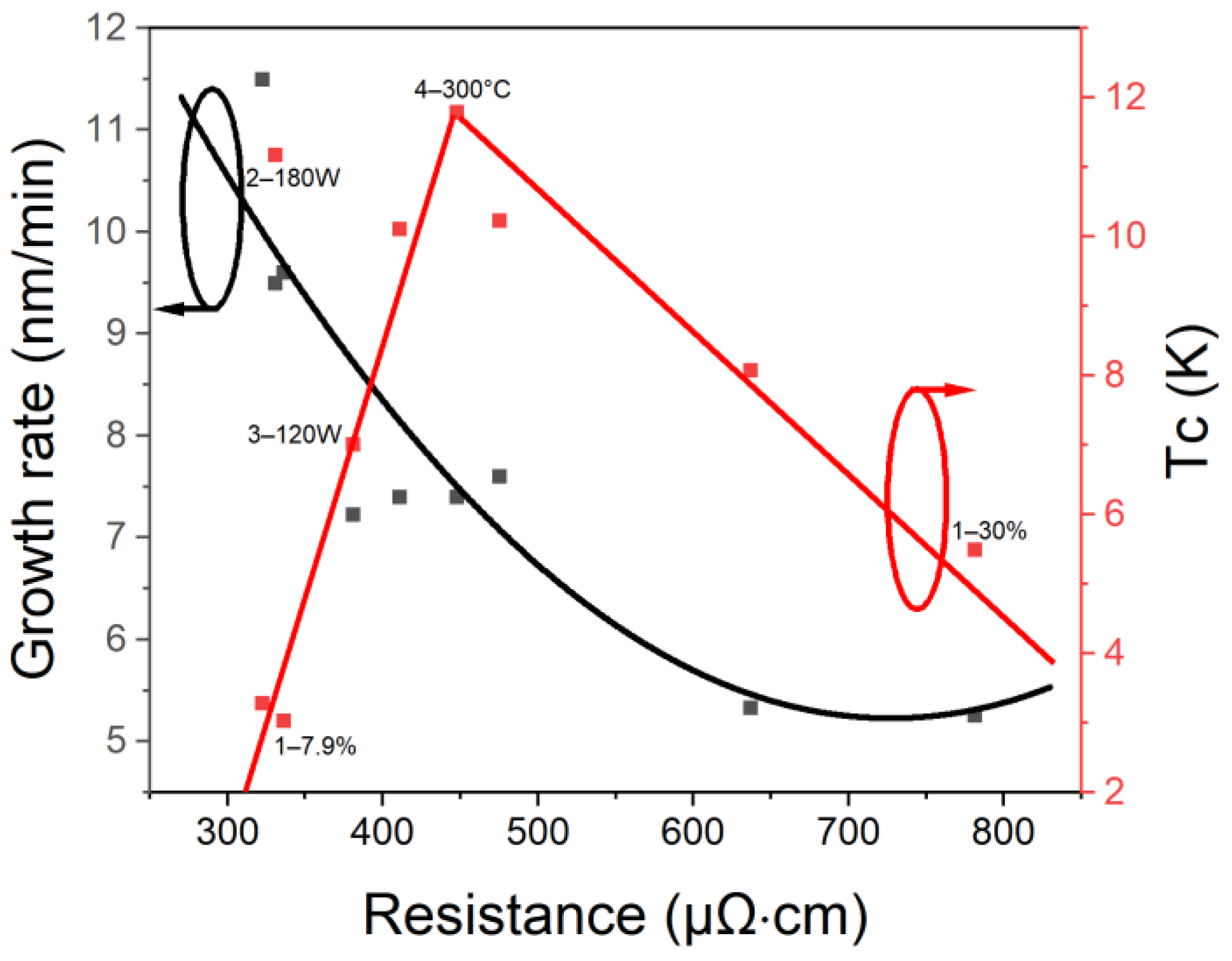
Figure 1 shows the relationship between resistance, growth rate, and Tc for all films from Series 1 to Series 4. As the resistance of the prepared films increased, their growth rate gradually decreased, and the superconducting performance presented first an increase and then a decreasing trend. This result suggests that the electrical resistivity of the sputtered NbN films could preliminarily judge the superconductivity. When the resistance of the thin film was close to 400–500 μΩ·cm, it exhibited a higher Tc.
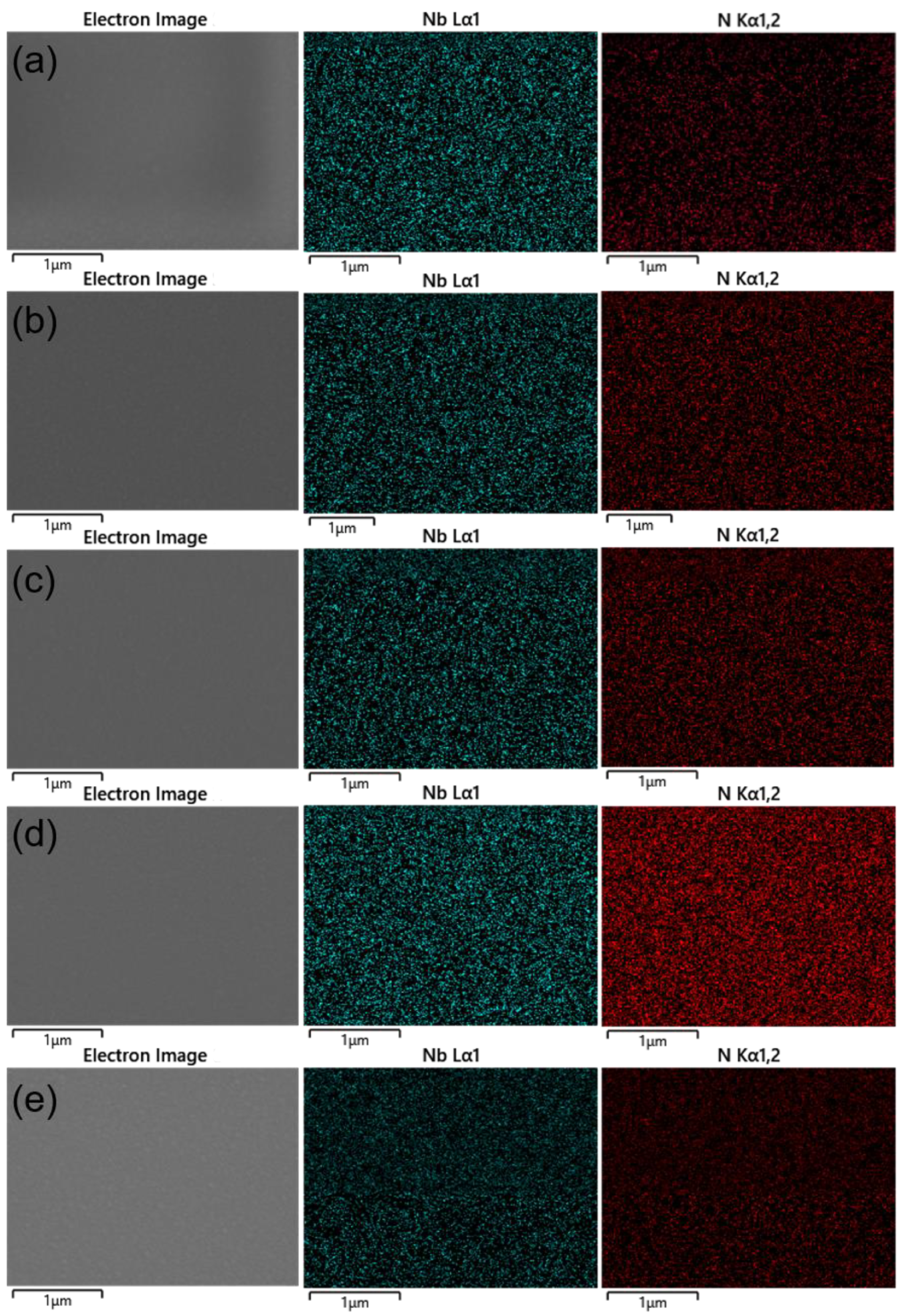
Figure 2 shows the SEM test results of (a) 1%–7.9%, (b) 3–120 W, (c) 4–300 °C, (d) 1–30%, and (e) 2–180 W, which are marked in Figure 1. From the SEM test results, the surface topography of 1%–7.9%, 3–120 W, 4–300 °C, and 1%–30% was similar, and was relatively smooth. However, visible crystalline grains could be observed on the surface of 2–180 W, which may be the reason why 2–180 W deviated from the trend line in Figure 1. The EDS test results revealed the elemental composition of the samples, showing the following sequence of N/Nb ratio in films: x1–7.9% << x3–120 W < x2–180 W < x4–300 °C << x1–30%. This indicated that as the N/Nb ratio in the films increased, their resistivity increased while the growth rate decreased. Increasing the Nb composition in the films possibly made the properties of the film closer to a Nb-rich NbN and, since the resistance of bulk Nb is much smaller than bulk NbN, this may be the reason why the electrical resistance decreased with the Nb-rich NbN thin film. Moreover, only when the N/Nb ratio was within an appropriate range was the superconducting performance of the film optimal, which is consistent with previous research. Among the phases of the NbN, δ-NbN formed when the ratio of nitrogen (N) atoms to niobium (Nb) atoms was close to 0.91 in the films and had the highest Tc [37]. Increasing the nitrogen partial pressure in the chamber led to more nitrogen ions nearing the substrate surface and participating in reactions, which led to an increase in the N/Nb ratio in the films. In addition, increasing the sputtering power led to more Nb atoms reaching the sample surface and participating in reactions by promoting the ionization of argon (Ar) atoms, which, in turn, increased the number of Nb atoms that were ejected from the target and the Nb atoms in films. However, a higher amount of Nb atoms sputtering from the target could also cause an imbalance in the elemental composition of the resulting film, especially in an environment lacking nitrogen, just like the films in Series 2. Increasing the growth temperature was helpful to slightly increase the nitrogen composition in the film, but too high a growth temperature also led to nitrogen desorption, as discussed by Zhang et al. [20].
For the growth rate, increasing the sputtering power boosted the energy and velocity of the ions and atoms in the chamber, which led to more particles reaching the surface of the substrate per minute. As the N2/Ar ratio in the chamber increased, the hysteresis phenomenon [38] occurred, and the deposition rate gradually decreased. Increasing the N2/Ar ratio in the chamber led to a higher N content in the films and a lower growth rate, while raising the power resulted in a higher Nb content in the films and a higher growth rate. This explained the variation in the growth rate of the films with changes in elemental composition.
The above result indicated that it is feasible to control the composition of elements in thin films by adjusting process parameters, thereby controlling the Tc and resistivity of the thin film. However, this method also has some drawbacks, as shown in Figure 1. It could be observed that fabricating high-resistance NbN thin films at high growth rates is difficult. This limitation may restrict the industrial applications of high-resistance NbN thin films. Furthermore, this also implies that it is very challenging to fabricate films with high Tc and high resistance or high Tc and low resistance, which are both useful for different applications, by adjusting the sputtering process parameters. Sample 2–180 W demonstrated that the crystalline quality of the film also affected the superconducting transition temperature and resistivity. The substrates and/or buffer layers used in magnetron sputtering and post-treatment impact the crystalline quality, and thus may also affect the superconducting properties and electrical properties of NbN films, which are potential solutions to overcome the limitations of only adjusting the sputtering process parameters.
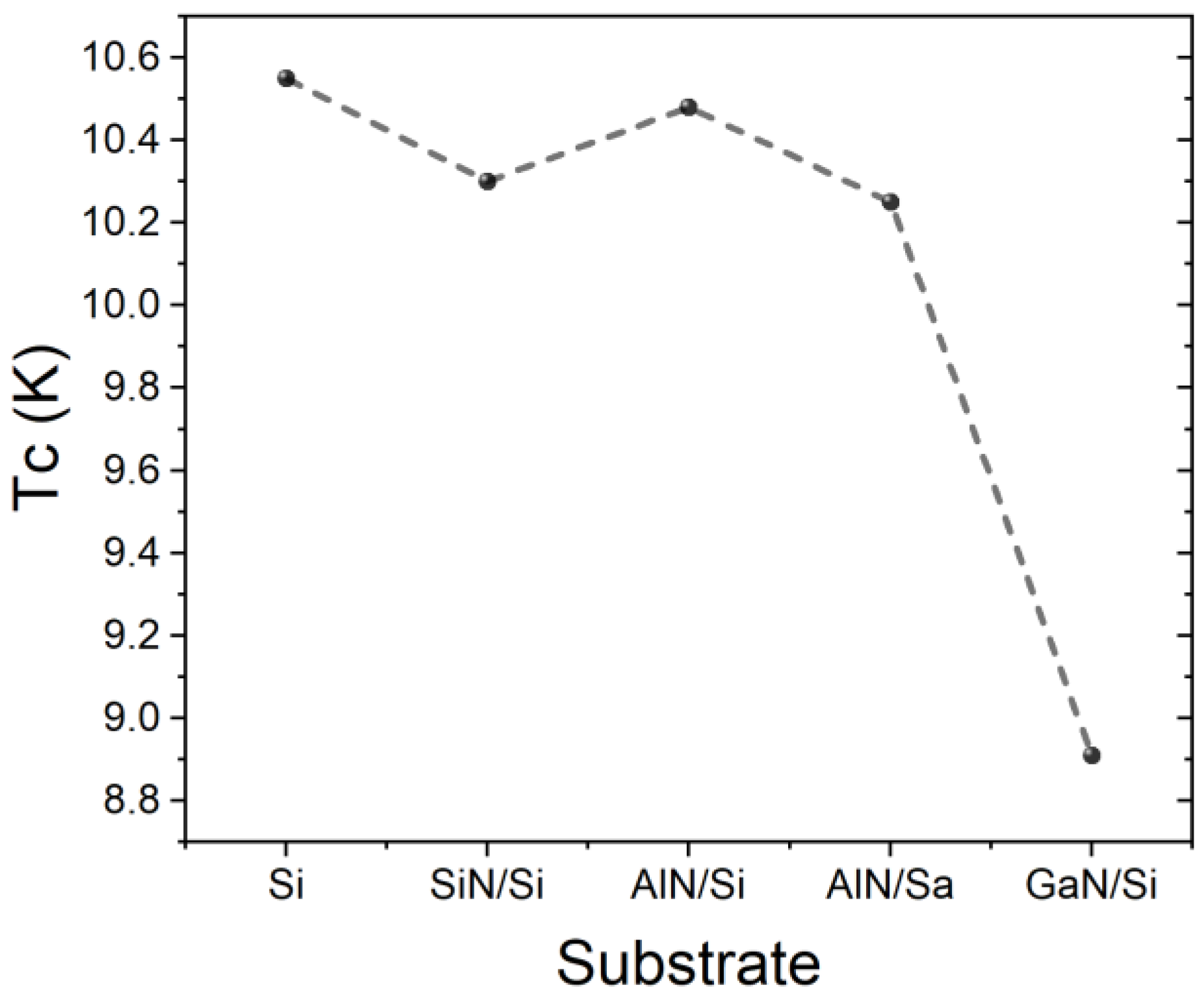
Figure 3 shows the Tc of NbN films in Series 5 and 5-NbN-Si after annealing. Except for the Tc of NbN on GaN being 8.9 K, which was significantly lower than that of films on other substrates, the Tc values of films on other substrates were very close. The Tc values of NbN/Si, NbN/SiN/Si, NbN/AlN/Si, and NbN/AlN/sapphire were 10.55 K, 10.3 K, 10.5 K, and 10.25 K, respectively.
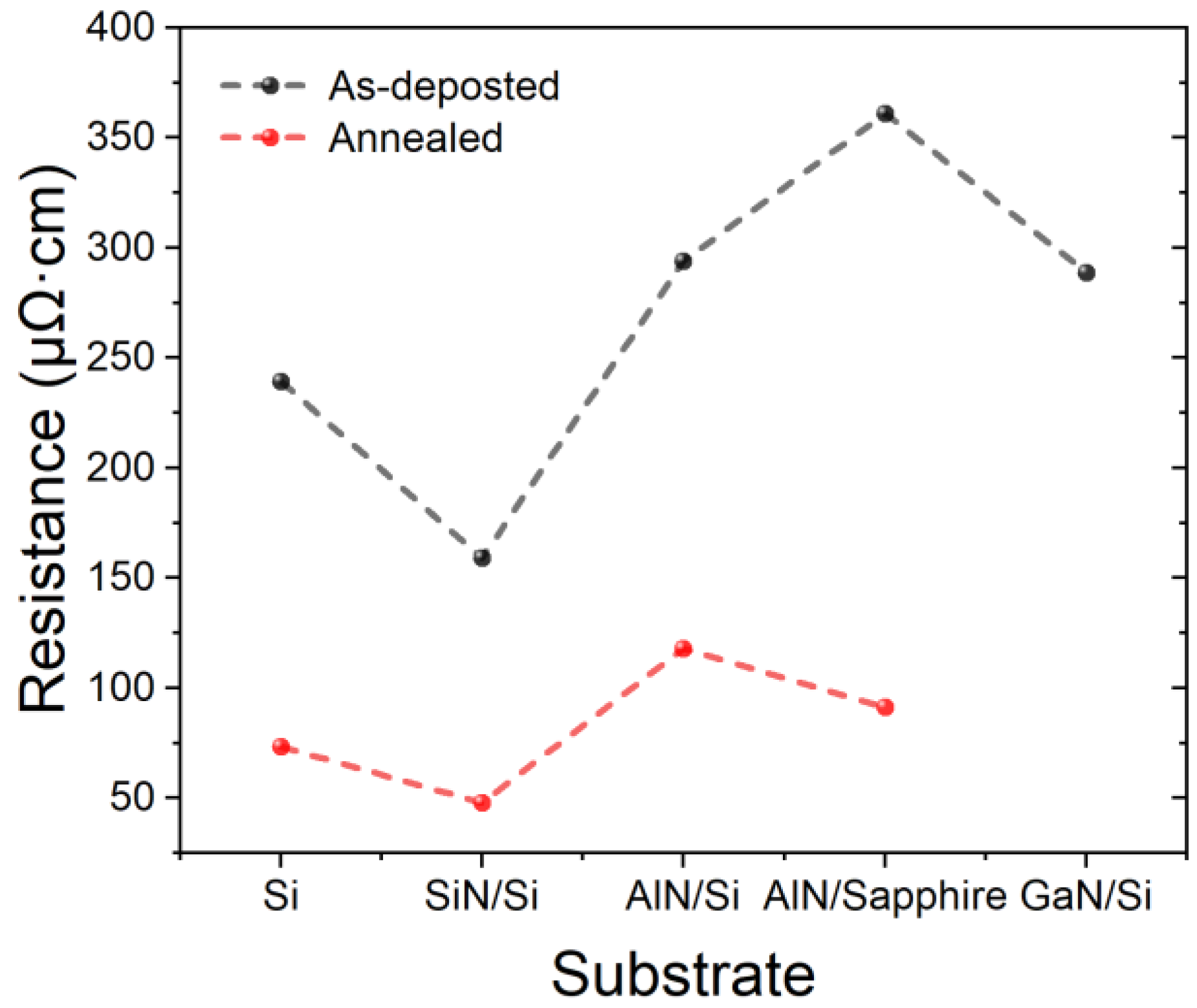
Annealing is the most common post-processing method. Figure 4 shows the electrical resistance of NbN films in Series 5 before and after annealing, which indicates that the substrates and buffer layers significantly influenced the electrical resistance of the NbN films. After annealing at 900 °C, the NbN film on the GaN buffer layer almost completely delaminated from the substrate, revealing a purple GaN buffer layer. This phenomenon may be attributed to the relatively low adhesion on the GaN buffer layer compared to other substrates, which may lead to poor superconductivity. After annealing, the resistivity of the films on all other substrates was significantly reduced, and the Tc of NbN/AlN/Si increased from 10.5 K to 15.5 K, indicating that annealing could significantly increase the superconducting property and reduce the resistance of the films.
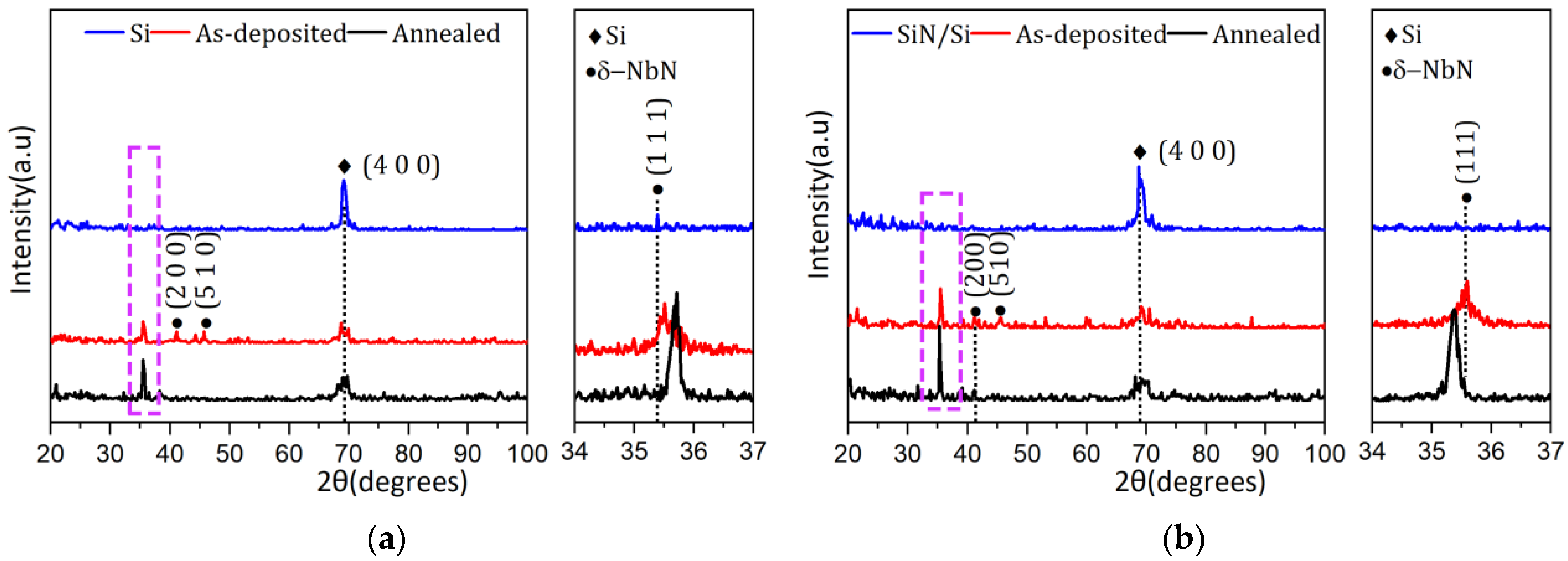
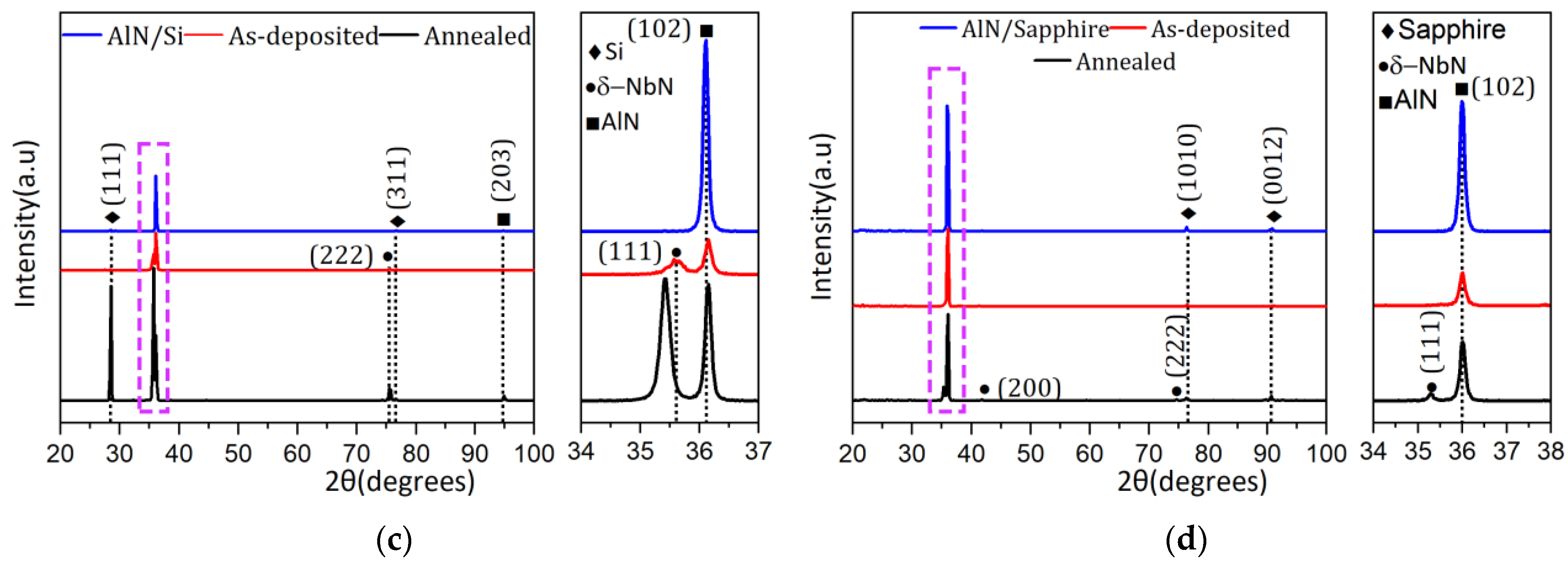
In order to investigate the crystal quality of films on different substrates before and after annealing, all the films in Series 5 were tested by XRD. Figure 5 presents XRD ω–2θ scans of these films and bare substrates. The smaller picture on the right side shows a higher resolution scan of the δ-NbN (111) peak around 36° obtained by decreasing the scan step size. On Si, SiN/Si, and AlN/Si substrates, the NbN film exhibited a peak at 2θ = 35.1°, which matched fairly well with the (111) reflections of δ-NbN (PDF# 00-038-1155). On the AlN/sapphire substrate, there was a very small δ-NbN (111) peak near the AlN(112) peak that was difficult to observe. On Si or SiN/Si substrates, peaks of δ-NbN (200) and (510) (PDF# 00-038-1155) could also be observed, which almost disappeared after annealing. In addition, a peak at around 71.5° could be found for NbN/AlN/Si, which represented (222) crystal planes of δ-NbN (PDF# 00-038-1155). The presence of secondary diffraction peaks, which are typically weak in signal and hard to observe with inferior quality thin films, suggested significantly improved crystalline quality of the film on the AlN buffer layer compared to the direct growth on the Si substrate. In addition, the thickness of the film on the AlN buffer layer was 193 nm, and the FWHM of the rocking curve of the δ-NbN (111) peak was 1.399°, which also suggested that the film on AlN/Si had a high degree of orientation. After annealing, the appearance of δ-NbN (111), δ-NbN (200), and δ-NbN (222) was observed on NbN/AlN/sapphire, which indicated that the crystal quality of the film was significantly improved. Due to the significant peak intensity of GaN itself and the similarity in 2θ angles between GaN and NbN peaks, it was challenging to distinguish the NbN peak in the XRD ω–2θ scans. Therefore, XRD patterns on this substrate are not displayed.
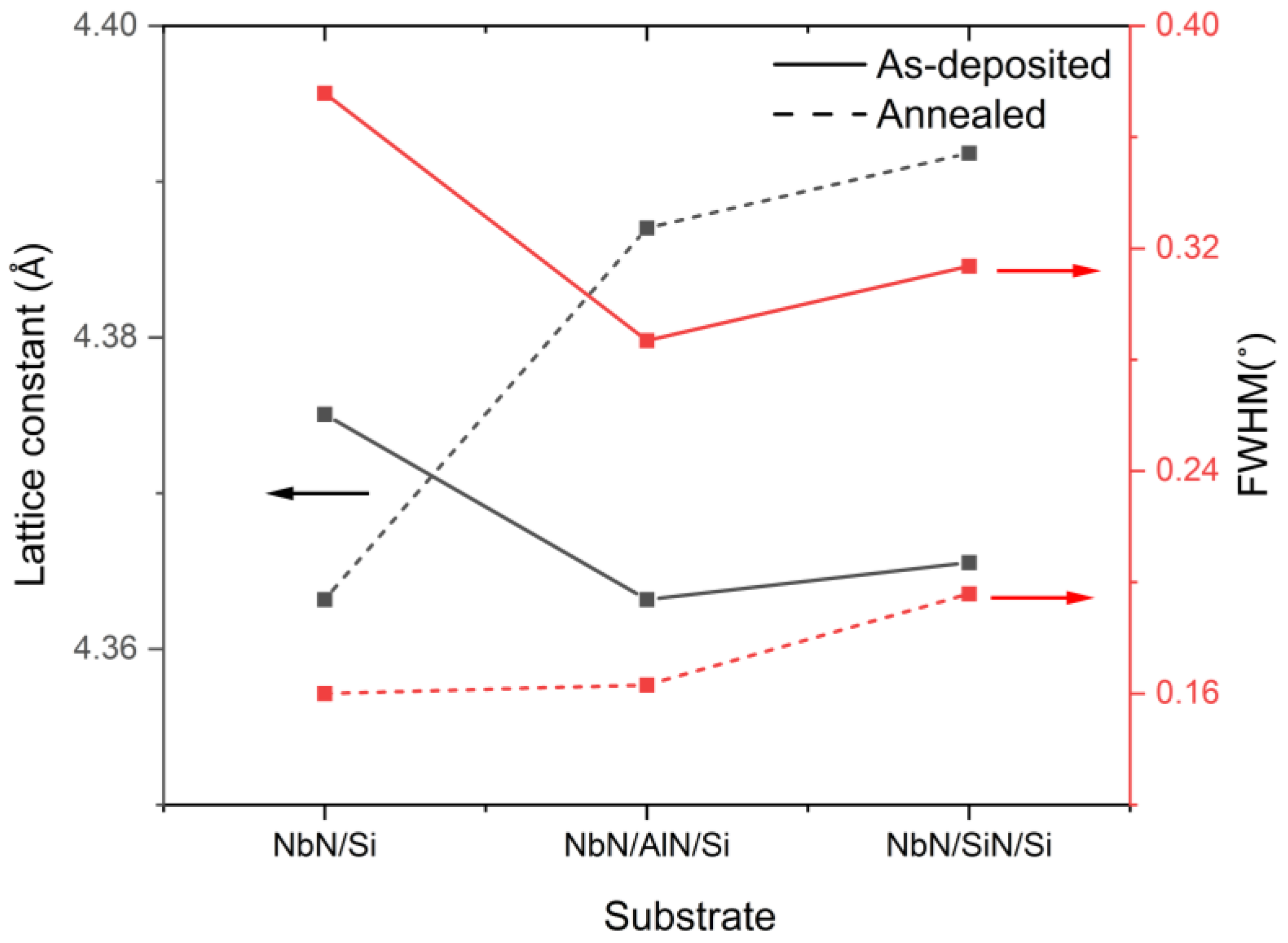
Figure 6 shows the lattice constants calculated by Bragg’s Law and the FWHM of films deposited on Si, AlN/Si, and SiN/Si substrates before and after annealing. Before annealing, using buffer layers significantly reduced the FWHM of NbN films on the Si substrate, which meant that the grain size of the NbN films increased according to the Scherrer equation. The grain size of NbN deposited on the AlN buffer layer seemed to be better than that on the SiN buffer layer. However, when using a buffer layer, there was a peak shift for δ-NbN (111), which meant that the out-of-plane lattice constant gradually deviated from the 4.39 Å of bulk NbN. The variation of the out-of-plane lattice constants may be attributed to the stress between the film and the buffer layer. Films with larger grain sizes should exhibit higher Tc. However, before annealing, the larger the grain size of the film, the more stress it experiences. The Tc values of these films were relatively close, which may be attributed to the significant stress between the film and the buffer layer, leading to the poorer superconducting performance of the films. After annealing, the FWHM of all the films significantly decreased, which meant that the grain size significantly increased. The out-of-plane lattice constant of films on SiN/Si and AlN/Si significantly increased and was close to the value of bulk NbN. However, the out-of-plane lattice constant of film on Si decreased after annealing. In addition, the 2θ angle of the δ-NbN (111) peak on AlN/sapphire also decreased after annealing. Annealing at an appropriate temperature could increase the grain size of thin films on all substrates and relieve stress on films on buffer layers, which may have improved the superconducting performance, which is consistent with the results reported in the literature [39].
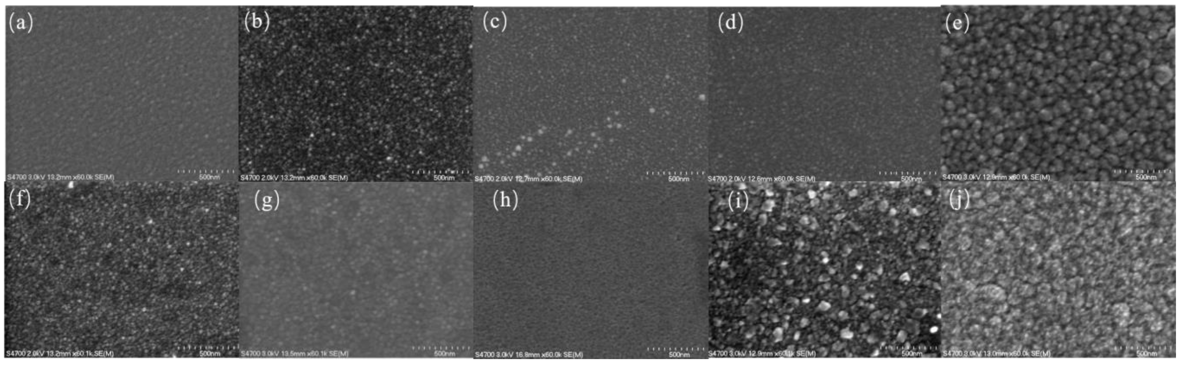
Figure 7 shows the SEM test results of films in Series 5 before and after annealing. The SEM test results shown in Figure 7 were obtained after annealing NbN/GaN/Si at 750 °C, as NbN/GaN/Si tended to peel off after annealing at 900 °C. Before annealing, the grain size of the film on the AlN/sapphire substrate was significantly larger than that on other substrates, indicating partial overlap between the peaks of δ-NbN (111) and AlN (102) before annealing. The larger peak angle of δ-NbN (111) suggested that the film was under greater stress. After annealing, the grain size and crystallinity of all films on the substrate except for the film on the GaN/Si substrate were significantly improved, consistent with the XRD test results. After annealing, it was difficult to observe grains on the surface of NbN/GaN/Si, and even some voids could be observed on its surface.
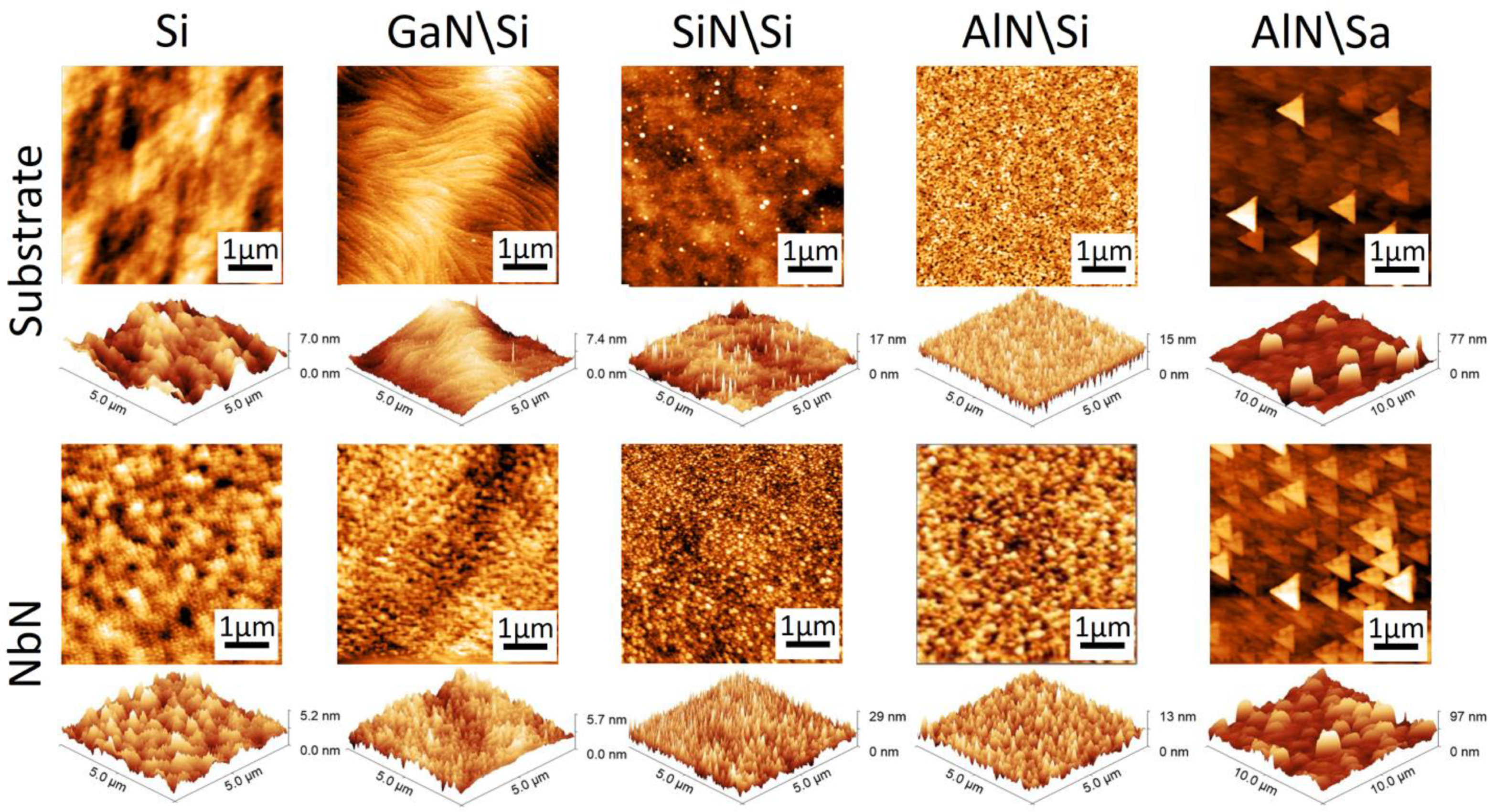
In addition to crystal quality, the surface topography of substrates can also affect the performance of thin films. To facilitate the study of the surface roughness of both the substrates and the thin films, Figure 8 shows the AFM test results of the films and substrates in Series 5. Table 2 summarizes the RMS of the test results. The morphology of the thin films was relatively similar to that of the substrates, with a small density of island structures observed. In addition, the AlN/sapphire substrate exhibited prominent triangular peaks and a significantly higher RMS value compared to other substrates. This may have significantly impacted the coherence and Tc at the bottom of the films, despite their relatively good surface crystal quality.
4. Conclusions
In the range of common process parameters, changes in process parameters have little effect on the crystal properties of films. The composition of the elements in a film will regularly affect the Tc, resistivity, and growth rate of the film. According to the mechanism of magnetron sputtering, the element composition of a film will also be significantly affected by the process parameters, providing a guiding scheme for simultaneously regulating the electrical properties and superconducting properties of films. However, it is difficult to prepare films with high Tc and high resistivity or high Tc and low resistivity by adjusting only the process parameters of films.
After adding a buffer layer, the crystal quality of the films prepared on AlN/sapphire, AlN/Si, and SiN/Si was higher, but the Tc values of the films prepared were similar due to greater stress or a rough substrate surface. After annealing at 900 °C, the stress of the films on the buffer layers was optimized significantly, but the stress of the film on the bare silicon substrate was increased. Annealing could increase the grain size and crystallinity of the films, except for the films on the GaN/Si substrates. This resulted in a significant decrease in the resistivity of the film and a significant increase in the superconducting transition temperature. The Tc of the AlN/Si films reached 15.51 K after annealing, which was close to the theoretical limit. Therefore, it is suggested that the process parameters be adjusted to prepare the film with the appropriate element composition. Subsequently, the crystallographic properties of the film can be refined through annealing to prepare NbN films with specific superconducting and electrical properties. This result provides valuable guidance for the fabrication of NbN films with specific superconducting and electrical properties.
Author Contributions
Conceptualization, Y.P. and X.G.; methodology, Y.P.; validation, X.G., Q.F., and X.N.; investigation, Y.P.; resources, X.G., Q.F., and X.N.; data curation, Y.P. and X.G.; writing—original draft preparation, Y.P.; writing—review and editing, X.G.; supervision, X.G.; project administration, X.G.; funding acquisition, X.G. All authors have read and agreed to the published version of the manuscript.
Funding
This research was funded by the National Nature Science Foundation of China, grant number 62074033.
Institutional Review Board Statement
Not applicable.
Informed Consent Statement
Informed consent was obtained from all subjects involved in the study.
Data Availability Statement
Data are contained within the article.
Conflicts of Interest
The authors declare no conflicts of interest.
References
- Cucciniello, N.; Lee, D.; Feng, H.Y.; Yang, Z.; Zeng, H.; Patibandla, N.; Zhu, M.; Jia, Q. Superconducting Niobium Nitride: A Perspective from Processing, Microstructure, and Superconducting Property for Single Photon Detectors. J. Phys. Condens. Matter 2022, 34, 374003. [Google Scholar] [CrossRef] [PubMed]
- Wei, X.; Roy, P.; Yang, Z.; Zhang, D.; He, Z.; Lu, P.; Licata, O.; Wang, H.; Mazumder, B.; Patibandla, N.; et al. Ultrathin Epitaxial NbN Superconducting Films with High Upper Critical Field Grown at Low Temperature. Mater. Res. Lett. 2021, 9, 336–342. [Google Scholar] [CrossRef]
- Pogrebnjak, A.D.; Bondar, O.V.; Abadias, G.; Ivashchenko, V.; Sobol, O.V.; Jurga, S.; Coy, E. Structural and Mechanical Properties of NbN and Nb-Si-N Films: Experiment and Molecular Dynamics Simulations. Ceram. Int. 2016, 42, 11743–11756. [Google Scholar] [CrossRef]
- Jia, X.Q.; Kang, L.; Gu, M.; Yang, X.Z.; Chen, C.; Tu, X.C.; Jin, B.B.; Xu, W.W.; Chen, J.; Wu, P.H. Fabrication of a Strain-Induced High Performance NbN Ultrathin Film by a Nb 5 N 6 Buffer Layer on Si Substrate. Supercond. Sci. Technol. 2014, 27, 035010. [Google Scholar] [CrossRef]
- Li, J.; Takeda, M.; Wang, Z.; Shi, S.C. Characterization of the Mixing Performance of All-NbN Superconducting Tunnel Junctions at 0.5 THz. IEEE Trans. Appl. Supercond. 2009, 19, 417–422. [Google Scholar] [CrossRef]
- Esmaeil Zadeh, I.; Chang, J.; Los, J.W.N.; Gyger, S.; Elshaari, A.W.; Steinhauer, S.; Dorenbos, S.N.; Zwiller, V. Superconducting Nanowire Single-Photon Detectors: A Perspective on Evolution, State-of-the-Art, Future Developments, and Applications. Appl. Phys. Lett. 2021, 118, 190502. [Google Scholar] [CrossRef]
- Il’in, K.S.; Stockhausen, A.; Scheuring, A.; Siegel, M.; Semenov, A.D.; Richter, H.; Huebers, H.-W. Technology and Performance of THz Hot-Electron Bolometer Mixers. IEEE Trans. Appl. Supercond. 2009, 19, 269–273. [Google Scholar] [CrossRef]
- Mazzocchi, F.; Ilin, K.; Kempf, S.; Kuzmin, A.; Strauß, D.; Scherer, T. Design and Comparison of Diamond- and Sapphire-Based NbN KIDs for Fusion Plasma Polarimetric Diagnostics. Physica Status Solidi (a) 2023, 220, 2200271. [Google Scholar] [CrossRef]
- Rhazi, R.; Machhadani, H.; Bougerol, C.; Lequien, S.; Robin, E.; Rodriguez, G.; Souil, R.; Thomassin, J.-L.; Mollard, N.; Désières, Y.; et al. Improvement of Critical Temperature of Niobium Nitride Deposited on 8-Inch Silicon Wafers Thanks to an AlN Buffer Layer. Supercond. Sci. Technol. 2021, 34, 045002. [Google Scholar] [CrossRef]
- Hazra, D.; Tsavdaris, N.; Jebari, S.; Grimm, A.; Blanchet, F.; Mercier, F.; Blanquet, E.; Chapelier, C.; Hofheinz, M. Superconducting Properties of Very High Quality NbN Thin Films Grown by High Temperature Chemical Vapor Deposition. Supercond. Sci. Technol. 2016, 29, 105011. [Google Scholar] [CrossRef]
- Shoji, A.; Kiryu, S.; Kohjiro, S. Superconducting Properties and Normal-State Resistivity of Single-Crystal NbN Films Prepared by a Reactive Rf-Magnetron Sputtering Method. Appl. Phys. Lett. 1992, 60, 1624–1626. [Google Scholar] [CrossRef]
- Babu, K.R. Electron-Phonon Coupling, Superconductivity, and Nontrivial Band Topology in NbN Polytypes. Phys. Rev. B 2019, 99, 104508. [Google Scholar] [CrossRef]
- Chaudhuri, S.; Nevala, M.R.; Hakkarainen, T.; Niemi, T.; Maasilta, I.J. Infrared Pulsed Laser Deposition of Niobium Nitride Thin Films. IEEE Trans. Appl. Supercond. 2011, 21, 143–146. [Google Scholar] [CrossRef]
- Chockalingam, S.P.; Chand, M.; Jesudasan, J.; Tripathi, V.; Raychaudhuri, P. Superconducting Properties and Hall Effect of Epitaxial NbN Thin Films. Phys. Rev. B 2008, 77, 214503. [Google Scholar] [CrossRef]
- Schneider, R.; Freitag, B.; Gerthsen, D.; Ilin, K.S.; Siegel, M. Structural, Microchemical and Superconducting Properties of Ultrathin NbN Films on Silicon. Cryst. Res. Technol. 2009, 44, 1115–1121. [Google Scholar] [CrossRef]
- Baskaran, R.; Thanikai Arasu, A.V.; Amaladass, E.P.; Janawadkar, M.P. High Upper Critical Field in Disordered Niobium Nitride Superconductor. J. Appl. Phys. 2014, 116, 163908. [Google Scholar] [CrossRef]
- Kobayashi, A.; Ueno, K.; Fujioka, H. Autonomous Growth of NbN Nanostructures on Atomically Flat AlN Surfaces. Appl. Phys. Lett. 2020, 117, 231601. [Google Scholar] [CrossRef]
- Semenov, A.; Günther, B.; Böttger, U.; Hübers, H.-W.; Bartolf, H.; Engel, A.; Schilling, A.; Ilin, K.; Siegel, M.; Schneider, R.; et al. Optical and Transport Properties of Ultrathin NbN Films and Nanostructures. Phys. Rev. B 2009, 80, 054510. [Google Scholar] [CrossRef]
- Makise, K.; Odou, T.; Ezaki, S.; Asano, T.; Shinozaki, B. Superconductor–Insulator Transition in Two-Dimensional NbN/MgO and NbN/AlN/MgO Films. Mater. Res. Express 2015, 2, 106001. [Google Scholar] [CrossRef]
- Zhang, K.; Balasubramanian, K.; Ozsdolay, B.D.; Mulligan, C.P.; Khare, S.V.; Zheng, W.T.; Gall, D. Growth and Mechanical Properties of Epitaxial NbN(001) Films on MgO(001). Surf. Coat. Technol. 2016, 288, 105–114. [Google Scholar] [CrossRef]
- Licata, O.G.; Sarker, J.; Bachhav, M.; Roy, P.; Wei, X.; Yang, Z.; Patibandla, N.; Zeng, H.; Zhu, M.; Jia, Q.; et al. Correlation between Thickness Dependent Nanoscale Structural Chemistry and Superconducting Properties of Ultrathin Epitaxial NbN Films. Mater. Chem. Phys. 2022, 282, 125962. [Google Scholar] [CrossRef]
- Zhang, J.J.; Su, X.; Zhang, L.; Zheng, L.; Wang, X.F.; You, L. Improvement of the Superconducting Properties of NbN Thin Film on Single-Crystal Silicon Substrate by Using a TiN Buffer Layer. Supercond. Sci. Technol. 2013, 26, 045010. [Google Scholar] [CrossRef]
- Kim, S.; Terai, H.; Yamashita, T.; Qiu, W.; Fuse, T.; Yoshihara, F.; Ashhab, S.; Inomata, K.; Semba, K. Enhanced Coherence of All-Nitride Superconducting Qubits Epitaxially Grown on Silicon Substrate. Commun. Mater. 2021, 2, 98. [Google Scholar] [CrossRef]
- Krause, S.; Meledin, D.; Desmaris, V.; Pavolotsky, A.; Belitsky, V.; Rudziński, M.; Pippel, E. Epitaxial Growth of Ultra-Thin NbN Films on Alx Ga1− x N Buffer-Layers. Supercond. Sci. Technol. 2014, 27, 065009. [Google Scholar] [CrossRef]
- Tian, L.; Bottala-Gambetta, I.; Marchetto, V.; Jacquemin, M.; Crisci, A.; Reboud, R.; Mantoux, A.; Berthomé, G.; Mercier, F.; Sulpice, A.; et al. Improved Critical Temperature of Superconducting Plasma-Enhanced Atomic Layer Deposition of Niobium Nitride Thin Films by Thermal Annealing. Thin Solid Films 2020, 709, 138232. [Google Scholar] [CrossRef]
- Hotovy, I.; Buc, D.; Brcka, J.; Srnanek, R. Study of Niobium Nitride Films Produced by DC Reactive Magnetron Sputtering. Phys. Stat. Sol. (a) 1997, 161, 97–104. [Google Scholar] [CrossRef]
- Hotový, I.; Huran, J.; Búc, D.; Srnánek, R. Thermal Stability of NbN Films Deposited on GaAs Substrates. Vacuum 1998, 50, 45–48. [Google Scholar] [CrossRef]
- Katz, M.B.; Liu, C.-I.; Kruskopf, M.; Hill, H.M.; Hight Walker, A.R.; Elmquist, R.E.; Davydov, A.V.; Rigosi, A.F. Microstructural Evolution at the Interface of Superconducting Thin Films and SiC Substrate. MRS Commun. 2022, 12, 1168–1173. [Google Scholar] [CrossRef]
- Guziewicz, M.; Slysz, W.; Borysiewicz, M.; Kruszka, R.; Sidor, Z.; Juchniewicz, M.; Golaszewska, K.; Domagala, J.Z.; Rzodkiewicz, W.; Ratajczak, J.; et al. Technology of Ultrathin NbN and NbTiN Films for Superconducting Photodetectors. Acta Phys. Pol. A 2011, 120, A-76–A-79. [Google Scholar] [CrossRef]
- Hatano, M.; Nishino, T.; Kawabe, U. Effects of Thermal Annealing on Superconducting Nb and NbN Films. J. Vac. Sci. Technol. A Vac. Surf. Film. 1988, 6, 2381–2385. [Google Scholar] [CrossRef]
- Mazzocchi, F.; Driessen, E.; Shu, S.; Merker, M.; Ilin, K.; Siegel, M.; Meier, A.; Straus, D.; Scherer, T. Design of NbN Based Kinetic Inductance Detectors for Polarimetric Plasma Diagnostics. IEEE Trans. Appl. Supercond. 2021, 31, 1–7. [Google Scholar] [CrossRef]
- Mazzocchi, F.; Driessen, E.F.C.; Shu, S.; Grossetti, G.; Strauss, D.; Scherer, T. Development of NbN Polarization Sensitive KID for Fusion Applications. In Proceedings of the 2018 43rd International Conference on Infrared, Millimeter, and Terahertz Waves (IRMMW-THz), Nagoya, Japan, 9–14 September 2018; pp. 1–2. [Google Scholar]
- Ezaki, S.; Makise, K.; Shinozaki, B.; Odo, T.; Asano, T.; Terai, H.; Yamashita, T.; Miki, S.; Wang, Z. Localization and Interaction Effects in Ultrathin Epitaxial NbN Superconducting Films. J. Phys. 2012, 24, 475702. [Google Scholar] [CrossRef] [PubMed]
- Zhang, L.; You, L.; Chen, L.; Peng, W.; Wang, Z. Superconductivity of Disordered NbN Films Deposited on Magnesium Oxide and Oxidized Silicon Substrates. Supercond. Sci. Technol. 2022, 35, 105008. [Google Scholar] [CrossRef]
- Kang, L.; Jin, B.B.; Liu, X.Y.; Jia, X.Q.; Chen, J.; Ji, Z.M.; Xu, W.W.; Wu, P.H.; Mi, S.B.; Pimenov, A.; et al. Suppression of Superconductivity in Epitaxial NbN Ultrathin Films. J. Appl. Phys. 2011, 109, 033908. [Google Scholar] [CrossRef]
- Zhang, Q.; Wang, H.; Tang, X.; Peng, W.; Wang, Z. Superconductivity Dependence on Epitaxial NbN Film Thickness. IEEE Trans. Appl. Supercond. 2019, 29, 1–5. [Google Scholar] [CrossRef]
- Reithmaier, G.; Senf, J.; Lichtmannecker, S.; Reichert, T.; Flassig, F.; Voss, A.; Gross, R.; Finley, J.J. Optimisation of NbN Thin Films on GaAs Substrates for in-Situ Single Photon Detection in Structured Photonic Devices. J. Appl. Phys. 2013, 113, 143507. [Google Scholar] [CrossRef]
- Strijckmans, K.; Schelfhout, R.; Depla, D. Tutorial: Hysteresis during the Reactive Magnetron Sputtering Process. J. Appl. Phys. 2018, 124, 241101. [Google Scholar] [CrossRef]
- Marquardt, R.; Cipo, J.; Schlichting, F.; Kolhatkar, G.; Kohlstedt, H.; Kersten, H. Correlation between Properties of Direct Current Magnetron Sputtered Thin Niobium Nitride Films and Plasma Parameters. Thin Solid Films 2022, 742, 139046. [Google Scholar] [CrossRef]
Figure 1.
The relationship between resistance, growth rate (black squares), and Tc (red squares) for all films from Series 1 to Series 4.
Figure 1.
The relationship between resistance, growth rate (black squares), and Tc (red squares) for all films from Series 1 to Series 4.

Figure 2.
SEM and EDS test results of (a) 1%–7.9%, (b) 3–120 W, (c) 4–300 °C, (d) 1%–30%, and (e) 2–180 W, which are marked in Figure 1.
Figure 2.
SEM and EDS test results of (a) 1%–7.9%, (b) 3–120 W, (c) 4–300 °C, (d) 1%–30%, and (e) 2–180 W, which are marked in Figure 1.

Figure 3.
Tc of NbN films in Series 5.

Figure 4.
Electrical resistance of NbN films in Series 5 before and after annealing.

Figure 5.
XRD ω–2θ scans of (a) Si, (b) SiN/Si, (c) AlN/Si, and (d) AlN/sapphire substrates. NbN films were deposited on the substrates and the films were annealed at 900 °C. The smaller picture on the right side (purple dotted square in the left picture) shows a higher resolution scan of the δ-NbN (111) peak at around 36° obtained by decreasing the scan step size.


Figure 6.
The lattice constants (black) and FWHM (red) of films deposited on Si, AlN/Si, and SiN/Si substrates before and after annealing.
Figure 6.
The lattice constants (black) and FWHM (red) of films deposited on Si, AlN/Si, and SiN/Si substrates before and after annealing.

Figure 7.
The SEM of films deposited on Si (a) before and (f) after 900 °C annealing, SiN/Si (b) before and (g) after 900 °C annealing, GaN/Si (c) before and (h) after 750 °C annealing, AlN/Si (d) before and (i) after 900 °C annealing, and AlN/sapphire (e) before and (j) after 900 °C annealing.
Figure 7.
The SEM of films deposited on Si (a) before and (f) after 900 °C annealing, SiN/Si (b) before and (g) after 900 °C annealing, GaN/Si (c) before and (h) after 750 °C annealing, AlN/Si (d) before and (i) after 900 °C annealing, and AlN/sapphire (e) before and (j) after 900 °C annealing.

Figure 8.
The AFM test results of Si, GaN/Si, SiN/Si, AlN/Si, and AlN/sapphire and NbN films deposited on them.
Figure 8.
The AFM test results of Si, GaN/Si, SiN/Si, AlN/Si, and AlN/sapphire and NbN films deposited on them.


Table 1.
The sputtering power, growth temperature, N2/Ar ratio, Tc, growth rate, and resistance of films in Series 1 to Series 4.
Table 1.
The sputtering power, growth temperature, N2/Ar ratio, Tc, growth rate, and resistance of films in Series 1 to Series 4.
| Samples | Power (W) | Temperature (°C) | N2/Ar | Tc (K) | Growth Rate (nm/min) | Resistance (μΩ·cm) |
|---|---|---|---|---|---|---|
| 1%–30% | 150 | 500 | 30% | 5.5 | 5.2 | 781 |
| 1%–17.1%, 2–150 W, 4–500 °C | 150 | 500 | 17.1% | 10.2 | 7.6 | 475 |
| 1%–7.9%, 3–150 W | 150 | 500 | 7.9% | 3 | 9.6 | 336 |
| 2–120 W | 120 | 500 | 17.1% | 8.1 | 4.9 | 636 |
| 2–180 W | 180 | 500 | 17.1% | 11.2 | 9.5 | 330 |
| 3–120 W | 120 | 500 | 7.9% | 7 | 7.2 | 380 |
| 3–180 W | 180 | 500 | 7.9% | 3.3 | 11.5 | 322 |
| 4–600 °C | 150 | 600 | 17.1% | 10.1 | 7.4 | 410 |
| 4–300 °C | 150 | 300 | 17.1% | 11.8 | 7.4 | 447 |
Table 2.
The RMS (nm) of films and bare substrates in Series 5.
| Si | GaN/Si | SiN/Si | AlN/Si | AlN/Sapphire | |
|---|---|---|---|---|---|
| Substrate | 1.1 | 0.46 | 1.4 | 1.7 | 9.2 |
| As-deposited film | 0.7 | 0.67 | 3.4 | 1.4 | 12 |
Disclaimer/Publisher’s Note: The statements, opinions and data contained in all publications are solely those of the individual author(s) and contributor(s) and not of MDPI and/or the editor(s). MDPI and/or the editor(s) disclaim responsibility for any injury to people or property resulting from any ideas, methods, instructions or products referred to in the content. |
© 2024 by the authors. Licensee MDPI, Basel, Switzerland. This article is an open access article distributed under the terms and conditions of the Creative Commons Attribution (CC BY) license (https://creativecommons.org/licenses/by/4.0/).
Share and Cite
MDPI and ACS Style
Pei, Y.; Fan, Q.; Ni, X.; Gu, X. Controlling the Superconducting Critical Temperature and Resistance of NbN Films through Thin Film Deposition and Annealing. Coatings 2024, 14, 496. https://doi.org/10.3390/coatings14040496
AMA Style
Pei Y, Fan Q, Ni X, Gu X. Controlling the Superconducting Critical Temperature and Resistance of NbN Films through Thin Film Deposition and Annealing. Coatings. 2024; 14(4):496. https://doi.org/10.3390/coatings14040496
Chicago/Turabian StylePei, Yang, Qian Fan, Xianfeng Ni, and Xing Gu. 2024. "Controlling the Superconducting Critical Temperature and Resistance of NbN Films through Thin Film Deposition and Annealing" Coatings 14, no. 4: 496. https://doi.org/10.3390/coatings14040496
Note that from the first issue of 2016, this journal uses article numbers instead of page numbers. See further details here.