
Study on Saturable Absorption Characteristics of Bi2Se3 Topological Insulators with Film Thickness Dependence and Its Laser Application

 ,
,
Abstract
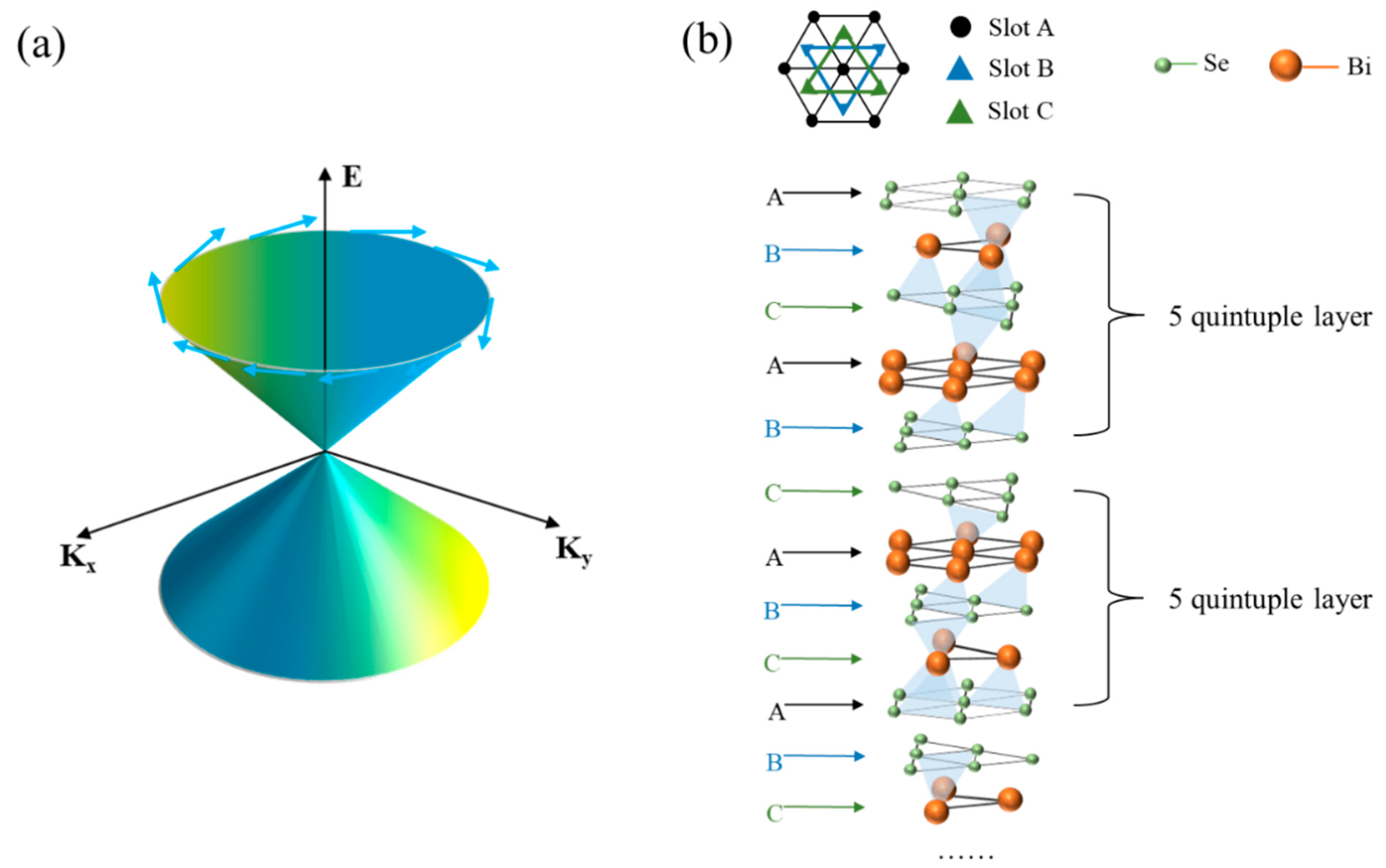
:1. Introduction
2. Experimental Section
2.1. Preparation and Characterization of TI Sample
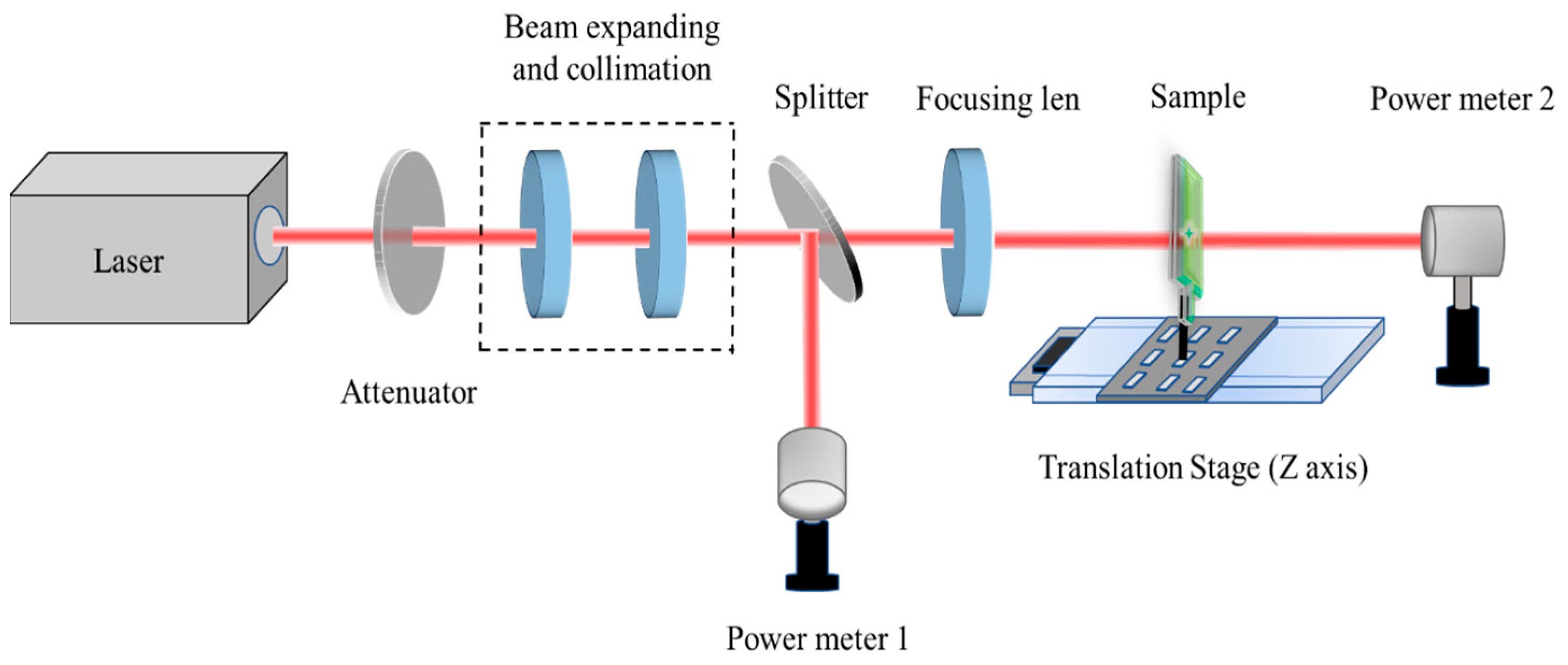
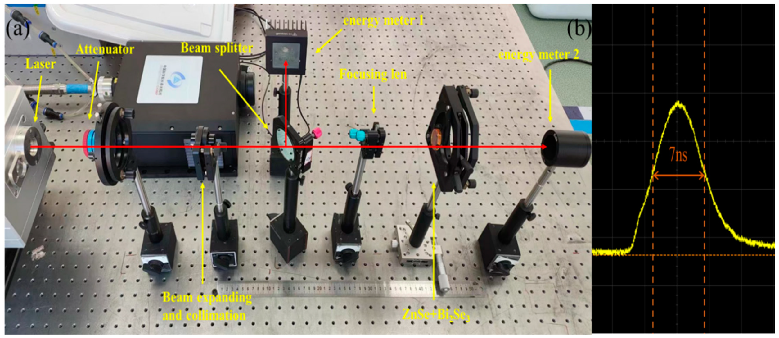
2.2. Experimental Setup
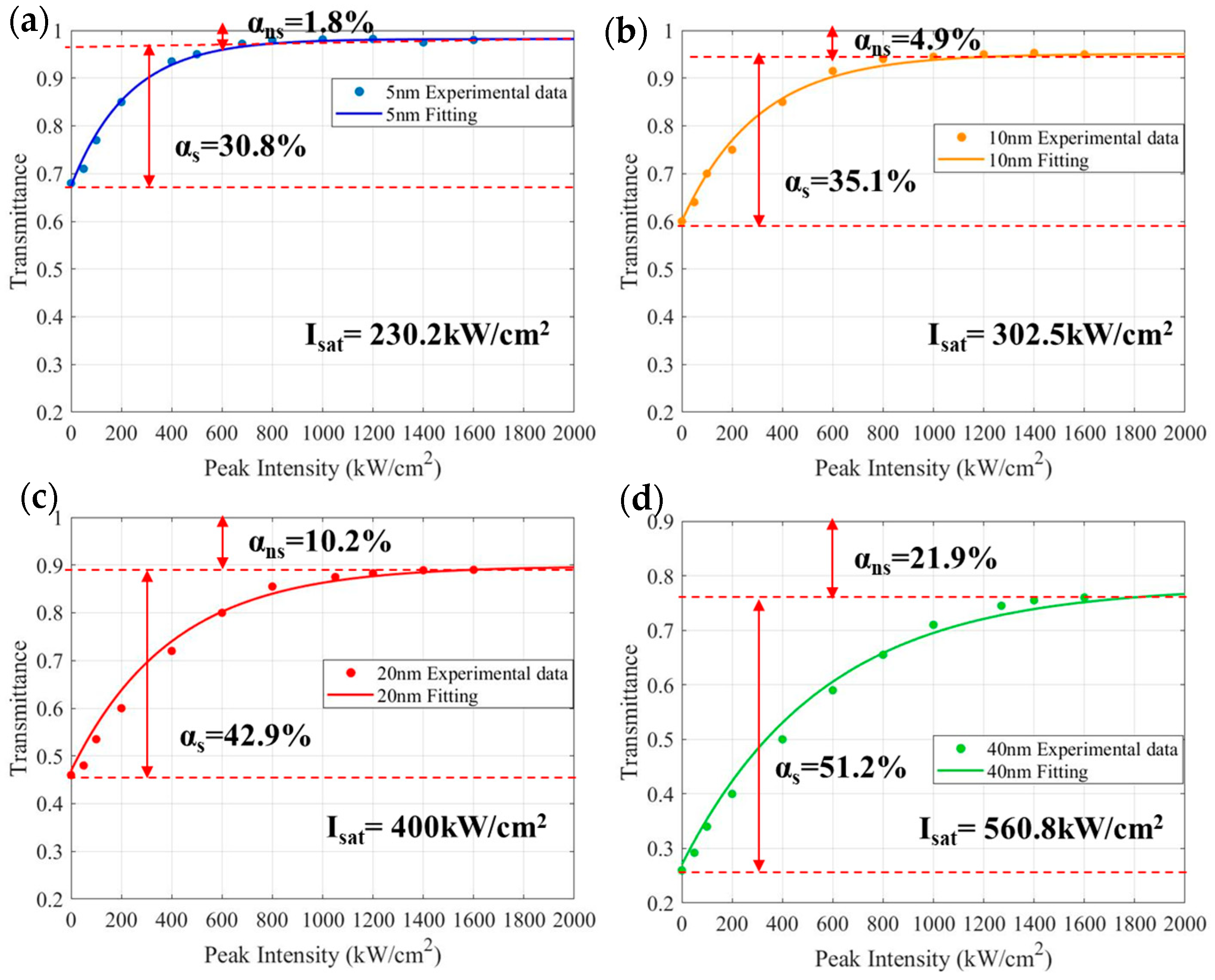
3. Saturable Absorption Parameters
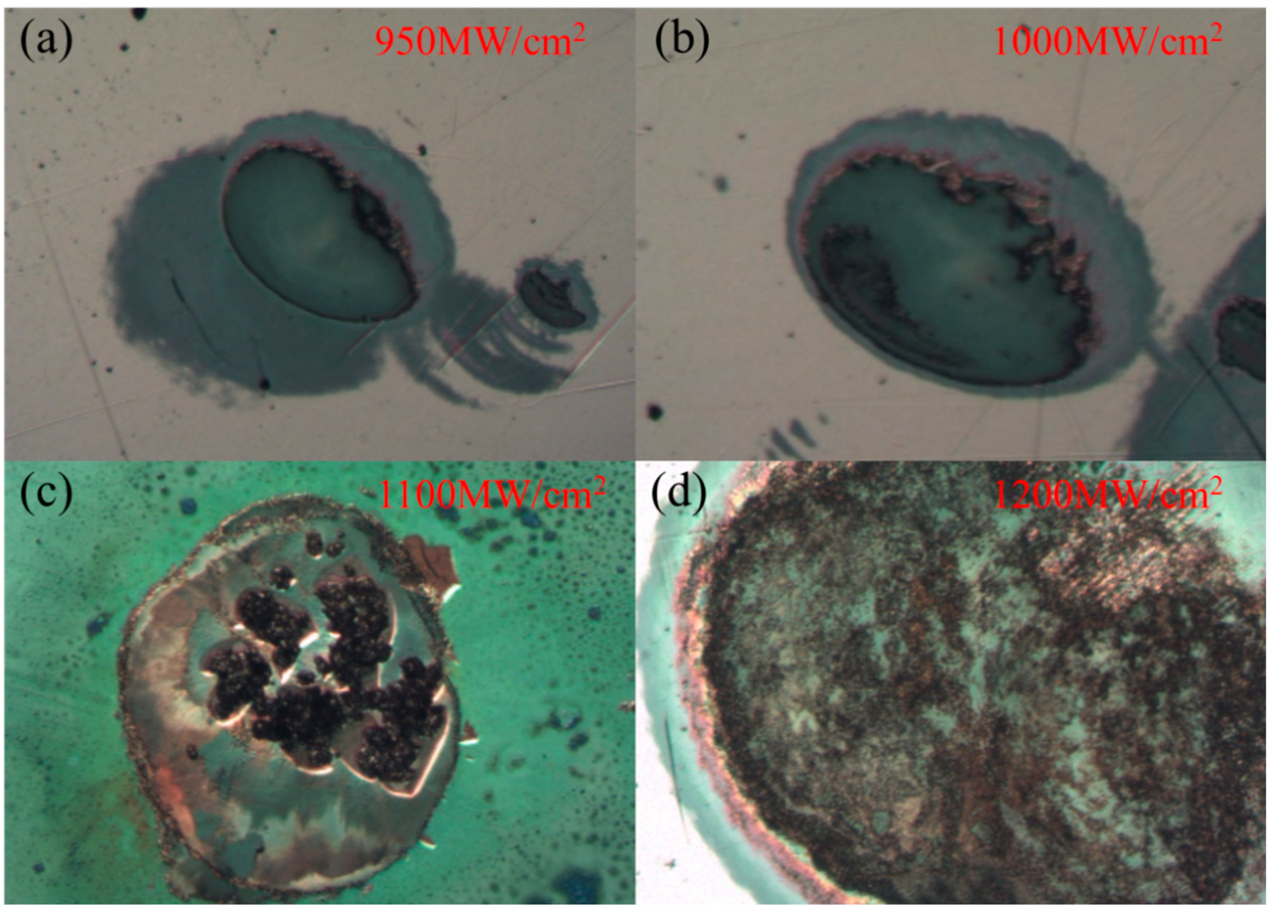
4. Damage Threshold
5. Laser Application
5.1. Q-Switching or Mode-Locking
5.2. The 1064 nm TI:Bi2Se3 Isolator
6. Conclusions
Author Contributions
Funding
Institutional Review Board Statement
Informed Consent Statement
Data Availability Statement
Conflicts of Interest
References
- Li, J.; Yan, J.; Jiang, L. Nanoscale multi-beam lithography of photonic crystals with ultrafast laser. Light Sci. Appl. 2023, 12, 164. [Google Scholar] [CrossRef] [PubMed]
- Fermann, M.E.; Hartl, I. Ultrafast fibre lasers. Nat. Photonics 2013, 7, 868–874. [Google Scholar] [CrossRef]
- Xu, S.C.; Man, B.Y.; Jiang, S.Z. Direct growth of graphene on quartz substrate as saturable absorber for femtosecond solid-state laser. Laser Phys. Lett. 2014, 11, 085801. [Google Scholar] [CrossRef]
- Niu, K.; Sun, R.; Chen, Q. Passively mode-locked Er-doped fiber laser based on SnS2 nanosheets as a saturable absorber. Photonics Res. 2018, 6, 72–76. [Google Scholar] [CrossRef]
- Li, L.; Pang, L.; Zhao, Q. VSe2 nanosheets for ultrafast fiber lasers. J. Mater. Chem. C 2020, 8, 1104–1109. [Google Scholar] [CrossRef]
- Yang, Z.; Yu, Q.; Wu, J. Ultrafast laser state active controlling based on anisotropic quasi-1D material. Light Sci. Appl. 2024, 13, 81. [Google Scholar] [CrossRef]
- Bao, Q.; Zhang, H.; Wang, Y. Atomic-layer graphene as a saturable absorber for ultrafast pulsed lasers. Adv. Funct. Mater. 2009, 19, 3077–3083. [Google Scholar] [CrossRef]
- Lau, K.Y.; Qiu, J. Broad applications of sensors based on laser-scribed graphene. Light Sci. Appl. 2023, 12, 168. [Google Scholar] [CrossRef] [PubMed]
- Zhou, D.P.; Wei, L.; Dong, B. Tunable passively Q-switched erbium-doped fiber laser with carbon nanotubes as a saturable absorber. IEEE Photonics Technol. Lett. 2009, 22, 9–11. [Google Scholar] [CrossRef]
- Xu, N.; Ming, N.; Han, X. Large-energy passively Q-switched Er-doped fiber laser based on CVD-Bi2Se3 as saturable absorber. Opt. Mater. Express 2019, 9, 373–383. [Google Scholar] [CrossRef]
- Haris, H.; Batumalay, M.; Tan, S.J. Mode-locked YDFL using topological insulator bismuth selenide nanosheets as the saturable absorber. Crystals 2022, 12, 489. [Google Scholar] [CrossRef]
- Wang, X.; Xu, J.; Sun, Y. Near infrared passively Q-switched solid state laser based on Sb2Te3 topological insulator saturable absorber. J. Lumin. 2017, 192, 1–5. [Google Scholar] [CrossRef]
- Wei, Q.; Han, X.; Zhang, H. CVD-Bi2Te3 as a saturable absorber for various solitons in a mode-locked Er-doped fiber laser. Appl. Opt. 2020, 59, 7792–7800. [Google Scholar] [CrossRef] [PubMed]
- Miao, L.; Yi, J.; Wang, Q. Broadband third order nonlinear optical responses of bismuth telluride nanosheets. Opt. Mater. Express 2016, 6, 2244–2251. [Google Scholar] [CrossRef]
- Wu, Y.; Mi, Z. Topological Dirac-vortex microcavity laser for robust on-chip optoelectronics. Light Sci. Appl. 2024, 13, 64. [Google Scholar] [CrossRef] [PubMed]
- Liu, M.; Wu, H.; Liu, X. Optical properties and applications of SnS2 SAs with different thickness. Opto-Electron. Adv. 2021, 4, 200029-1–200029-10. [Google Scholar] [CrossRef]
- Li, L.; Pang, L.; Wang, R. Ternary transition metal dichalcogenides for high power vector dissipative soliton ultrafast fiber laser. Laser Photonics Rev. 2022, 16, 2100255. [Google Scholar] [CrossRef]
- Hisyam, M.B.; Rusdi, M.F.M.; Latiff, A.A. Generation of mode-locked ytterbium doped fiber ring laser using few-layer black phosphorus as a saturable absorber. IEEE J. Sel. Top. Quantum Electron. 2016, 23, 39–43. [Google Scholar] [CrossRef]
- Markom, A.M.; Tan, S.J.; Muhammad, A.R. Dark pulse mode-locked fiber laser with zirconia-based erbium-doped fiber (Zr-EDF) and Black phosphorus saturable absorber. Optik 2020, 223, 165635. [Google Scholar] [CrossRef]
- Zhao, C.; Zhang, H.; Qi, X. Ultra-short pulse generation by a topological insulator based saturable absorber. Appl. Phys. Lett. 2012, 101, 211106. [Google Scholar] [CrossRef]
- Gao, L.; Zhu, T.; Huang, W. Stable, Ultrafast Pulse Mode-Locked by Topological Insulator Bi2Se3 Nanosheets Interacting with Photonic Crystal Fiber: From Anomalous Dispersion to Normal Dispersion. IEEE Photonics J. 2015, 7, 3300108. [Google Scholar] [CrossRef]
- Guo, B.; Yao, Y.; Yang, Y.F. Dual-wavelength rectangular pulse erbium-doped fiber laser based on topological insulator saturable absorber. Photonics Res. 2015, 3, 94–99. [Google Scholar] [CrossRef]
- Guo, B.; Yao, Y.; Tian, J.J. Observation of bright-dark soliton pair in a fiber laser with topological insulator. IEEE Photonics Technol. Lett. 2015, 27, 701–704. [Google Scholar] [CrossRef]
- Zhang, C.; Liu, M.; Man, B.Y. Facile fabrication of graphene-topological insulator Bi2Se3 hybrid Dirac materials via chemical vapor deposition in Se-rich conditions. CrystEngComm 2014, 16, 8941–8945. [Google Scholar] [CrossRef]
- Sun, Z.; Man, B.; Yang, C. Selenium-assisted controlled growth of graphene–Bi2Se3 nanoplates hybrid Dirac materials by chemical vapor deposition. Appl. Surf. Sci. 2016, 365, 357–363. [Google Scholar] [CrossRef]
- Zhang, H.; Liu, C.X.; Qi, X.L. Topological insulators in Bi2Se3, Bi2Te3 and Sb2Te3 with a single Dirac cone on the surface. Nat. Phys. 2009, 5, 438–442. [Google Scholar] [CrossRef]
- Zhao, C.; Zou, Y.; Chen, Y. Wavelength-tunable picosecond soliton fiber laser with topological insulator: Bi2Se3 as a mode locker. Opt. Express 2012, 20, 27888–27895. [Google Scholar] [CrossRef] [PubMed]
- Bernard, F.; Zhang, H.; Gorza, S.P. Towards mode-locked fiber laser using topological insulators. In Nonlinear Photonics; Optica Publishing Group: Washington, DC, USA, 2012; NTh1A. 5. [Google Scholar]
- Lu, S.; Zhao, C.; Zou, Y. Third order nonlinear optical property of Bi2Se3. Opt. Express 2013, 21, 2072–2082. [Google Scholar] [CrossRef] [PubMed]
- Pinghua, T.; Man, W.; Qingkai, W. 2.8-μm Pulsed Er 3+: ZBLAN fiber laser modulated by topological insulator. IEEE Photonics Technol. Lett. 2016, 28, 1573–1576. [Google Scholar]
- Wang, Q.; Chen, Y.; Jiang, G. Drop-casted self-assembled topological insulator membrane as an effective saturable absorber for ultrafast laser photonics. IEEE Photonics J. 2015, 7, 1500911. [Google Scholar] [CrossRef]
- Sun, Y.J.; Lee, C.K.; Xu, J.L. Passively Q-switched tri-wavelength Yb 3+: Gd Al 3(BO3)4 solid-state laser with topological insulator Bi2Te3 as saturable absorber. Photonics Res. 2015, 3, A97–A101. [Google Scholar] [CrossRef]
- Wang, J.; Zhang, K.; Yu, J. Electric Field Enhancement Effect of Aluminum Grating with Nanosecond Pulsed Laser Irradiation. Front. Phys. 2022, 10, 894925. [Google Scholar] [CrossRef]
- Zhang, R.; Pan, Q.; Xu, F. 10.6 μm saturable absorption and optical isolation of graphene. Infrared Phys. Technol. 2022, 122, 104080. [Google Scholar] [CrossRef]
- Qiao, Z.; Ma, P.; Liu, H. Laser-induced damage of rugate and quarter-wave stacks high reflectors deposited by ion-beam sputtering. Opt. Eng. 2013, 52, 086103. [Google Scholar] [CrossRef]
- Hönninger, C.; Paschotta, R.; Morier-Genoud, F. Q-switching stability limits of continuous-wave passive mode locking. JOSA B 1999, 16, 46–56. [Google Scholar] [CrossRef]
- Luo, Z.; Liu, C.; Huang, Y. Topological-insulator passively Q-switched double-clad Fiber laser at 2 μm wavelength. IEEE J. Sel. Top. Quantum Electron. 2014, 20, 0902708. [Google Scholar]


| Film Thickness (nm) | αs (%) | αns (%) | Isat (kW/cm2) |
|---|---|---|---|
| 5 | 30.8 | 1.8 | 230.2 |
| 10 | 35.1 | 4.9 | 302.5 |
| 20 | 42.9 | 10.2 | 400 |
| 40 | 51.2 | 21.9 | 560.8 |
| Film Thickness (nm) | Isat (kW/cm2) | LIDT (MW/cm2) |
|---|---|---|
| 5 | 230.2 | 909 |
| 10 | 302.5 | 57.1 |
| 20 | 400 | 16 |
| 40 | 560.8 | 2.72 |
Disclaimer/Publisher’s Note: The statements, opinions and data contained in all publications are solely those of the individual author(s) and contributor(s) and not of MDPI and/or the editor(s). MDPI and/or the editor(s) disclaim responsibility for any injury to people or property resulting from any ideas, methods, instructions or products referred to in the content. |
© 2024 by the authors. Licensee MDPI, Basel, Switzerland. This article is an open access article distributed under the terms and conditions of the Creative Commons Attribution (CC BY) license (https://creativecommons.org/licenses/by/4.0/).
Share and Cite
Gao, Y.; Chen, Y.; Zhang, R.; Pan, Q.; Zhao, C.; Zhou, Y.; Guo, J.; Chen, F. Study on Saturable Absorption Characteristics of Bi2Se3 Topological Insulators with Film Thickness Dependence and Its Laser Application. Coatings 2024, 14, 679. https://doi.org/10.3390/coatings14060679
Gao Y, Chen Y, Zhang R, Pan Q, Zhao C, Zhou Y, Guo J, Chen F. Study on Saturable Absorption Characteristics of Bi2Se3 Topological Insulators with Film Thickness Dependence and Its Laser Application. Coatings. 2024; 14(6):679. https://doi.org/10.3390/coatings14060679
Chicago/Turabian StyleGao, Yang, Yiyi Chen, Ranran Zhang, Qikun Pan, Chongxiao Zhao, Yiping Zhou, Jin Guo, and Fei Chen. 2024. "Study on Saturable Absorption Characteristics of Bi2Se3 Topological Insulators with Film Thickness Dependence and Its Laser Application" Coatings 14, no. 6: 679. https://doi.org/10.3390/coatings14060679