Article

Polarization-Dependent Plasmon Coupling in Gold Nanoparticles and Gold Thin-Film Systems

1
Department of Mathematics and Physics, Luoyang Institute of Science and Technology, Luoyang 471023, China
2
School of Environmental Engineering and Chemistry, Luoyang Institute of Science and Technology, Luoyang 471023, China
*
Author to whom correspondence should be addressed.
Coatings 2024, 14(6), 746; https://doi.org/10.3390/coatings14060746
Submission received: 11 May 2024 / Revised: 7 June 2024 / Accepted: 11 June 2024 / Published: 13 June 2024
(This article belongs to the Special Issue Thin-Film Synthesis, Characterization and Properties)

Abstract

:
The characteristics of gap plasmon formed by nanoparticle-on-mirror (NPOM) structures composed of metal nanoparticles (MNPs) and metal thin films have aroused interest for use in various optoelectronic devices. The resonance enhancement characteristics in the gap region of an NPOM structure composed of gold nanoparticles and gold thin films are simulated theoretically by the finite element method (FEM). The resonant spectrum obtained by the internal coupling effect of the gap can be flexibly controlled by the polarization of incident light and the thickness of the dielectric layer between the MNPs and the metal thin films. We study the resonance spectra of polarization-dependent gold ellipsoidal nanoparticles (GENPs) and gold thin films in the gap region of an NPOM structure. The GENPs and gold thin films are separated by a dielectric layer with a refractive index of 1.36. We observe that the intensity of the resonance electric field in the gap region is inversely proportional to the polarization angle. Similarly, the intensity of the local electric field resonance peak in the gap region is inversely proportional to the thickness of the dielectric layer. When the thickness of the dielectric layer is 0.3 nm and the polarization angle is 0°, the best resonant electric field intensity of 2200 V/m is obtained in the gap region of the NPOM structure (the power of incident light is 1 mW). Finally, the resonant peak wavelength of the electric field in the gap region of the NPOM structure is also controlled by the polarization angle of the incident light and the thickness of the dielectric layer.

1. Introduction

The localized surface plasmon resonance (LSPR) properties of metal nanoparticles (MNPs) have attracted wide attention. They have potential applications in solar cells, catalysis, surface-enhanced Raman scattering (SERS), fluorescence enhancement, biosensors, subwavelength imaging, random lasers and many other fields [1,2,3,4,5,6,7]. This process mainly makes use of the incident light-based excitation of the free electrons on the surface of the MNPs. When the frequency of the incident light is consistent with the oscillation frequency of the electrons on the MNP surface, surface plasmon resonance occurs [8,9,10]. The electric field on the surface of MNPs is greatly enhanced because of the resonance effect. The size and morphology of MNPs are closely related to the intensity of the local electric field [11,12,13]. Therefore, the surface electric field enhancement characteristics of MNPs are widely used in the field of plasmon modes and surface structures of materials [14,15].
Compared with the size of MNPs, the surface electric field intensity of MNPs is more affected by the morphology of the MNPs. It can affect the intensity of the resonance spectrum, the wavelength of the resonance peak and the width of the resonance spectrum. Studies have shown that in MNPs (nano-stars, nano-flowers, etc.) with a tip structure, because of the hot spot effect, a stronger electric field can be formed on the surface [16,17]. In addition, when two MNPs are close to each other, hot spots are also formed in their subwavelength gap region. Due to the coupling effect between MNPs, the local electric field intensity is higher than that on the surface of single-tip MNPs [18]. Similarly, when MNPs and metal thin films are close to each other to form nanoparticle-on-mirror (NPOM) structures, hot spots with strong local electric field enhancement appear in the gap region between them [19,20,21,22]. The electric field intensity in the gap region of an NPOM structure is greatly enhanced, and at the same time, it is accompanied by the broadening of the resonant spectrum and the shift in the resonant wavelength. The preparation of NPOM structures does not depend on complex equipment and also allows for good stability and tunability of the resonance peak, which makes them have potential applications in many fields. At present, scholars’ research on NPOM structures is mainly focused on the thickness of the dielectric layer between MNPs and metal thin films. When the thickness of the dielectric layer is less than 4 nm, there is only one gap mode in the NPOM structure. However, when the thickness is greater than 4 nm, both the gap mode and MNP mode appear [19]. The morphology of MNPs has a great influence on electric field resonance in the gap region. For example, when M. Lequeux studied [21] an NPOM structure composed of cylindrical nanoparticles, although the structural parameters of the cylindrical nanoparticles were changed, the resonance peak wavelength in the gap region could only be controlled in a small range. Therefore, it cannot be widely used in many application fields. Moreover, MNPs with various morphologies (ellipse, mushroom and bowtie) have been proposed to study the optical enhancement properties of NPOM structures [23,24,25]. Among the relevant studies, the most representative one is that by Jubb [23], who compared NPOM SERS substrates composed of three kinds of nanoparticles, i.e., ellipse, mushroom and bowtie. The results show that the Raman signal of ellipse nanoparticles is stronger than those of mushroom and bowtie nanoparticles. In fact, in addition to the thickness of the dielectric layer and the morphology of MNPs, the polarization angle of the light source can also affect the electric field enhancement characteristics of NPOM structures [26,27,28]. The coupling effect of two particles and the NPOM structure can produce strong electric field intensity in the hot spot region. However, in the preparation of the two structures, the subwavelength distance between the two adjacent MNPs needs to be accurately controlled by a physical method. This not only needs to rely on complex equipment but also has a high cost and takes a long time. The thickness of the dielectric layer in NPOM structures can be accurately controlled by the spin coating method, and various morphologies of MNPs can be prepared by chemical synthesis. To sum up, NPOM structures based on MNPs and metal thin films have a greater prospect.
In this paper, in order to study the strong resonance enhancement characteristics of NPOM structures, we establish the models of GENPs and gold thin films for calculation. An NPOM structure composed of gold nano-ellipsoid particles (GENPs) and gold thin films is studied theoretically with the help of the finite element method. Our aim is not only to improve the intensity of the resonant electric field but also to realize the accurate regulation of the resonant peak wavelength of the NPOM structure. Firstly, we compare and analyze the distribution characteristics of the electric field intensity on the surface of the GENPs in the homogeneous medium and the electric field intensity in the gap region of the NPOM structure. Then, it is found through analysis that the NPOM structures of three kinds of dielectric layer thickness are affected by the polarization angle of incident light. For each constant thickness of the dielectric layer, the variation characteristics of the electric field in the hot spot space are studied by changing six different polarization angles of incident light. Finally, the influence of the thickness of the dielectric layer of the NPOM structure on the intensity and wavelength of the local electric field resonance peak in the gap region is further studied. The NPOM structure has strong optical enhancement properties because of its coupling effect, which has potential applications in the fields of SERS, fluorescence enhancement, catalysis and so on.

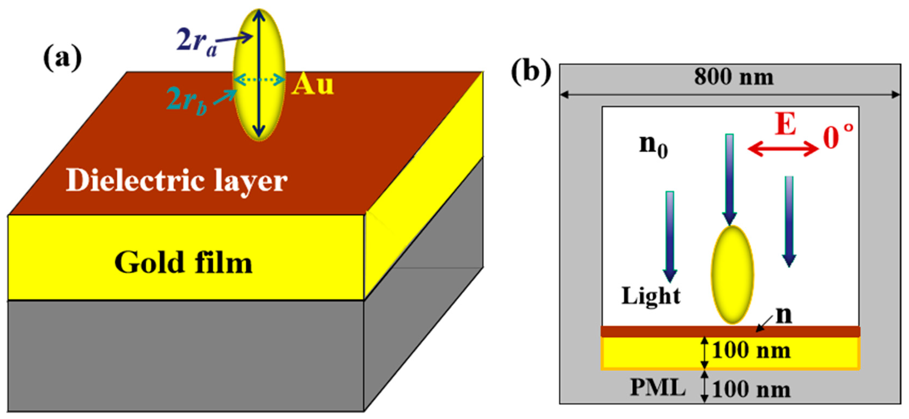
2. Simulation Model and Methods

The structural model diagram of the NPOM structure is shown in Figure 1a. The NPOM structure composed of GENPs and gold thin films is separated by the dielectric layer, and the thickness of the dielectric layer t can be adjusted arbitrarily. The aspect ratio of GENPs is 2, namely, ra = 2rb, where ra = 30 nm and rb = 15 nm. Throughout the article, the size and aspect ratio of the GENPs remain unchanged. The refractive index n0 around the GENPs in Figure 1b is 1, and the refractive index n of the dielectric layer is 1.36. When we build the model, the thickness size of the gold films is set to 100 nm. GENPs and gold thin films are composed of gold materials, and their optical parameters are from the literature [29]. The polarization angle of the incident light can be adjusted, and the polarization angle in the horizontal direction is 0°, as shown in Figure 1b. The construction and simulation of the theoretical model are completed in finite element simulation software. In order to verify the correctness of the simulation model, the simulation data of gold spherical nanoparticles are compared with the experimental data, and the results are shown in Figure S1 of the Supplementary Materials. In the process of calculation, the model needs to be meshed. The smaller the mesh size is, the better the convergence of the calculation results is, and the more accurate the calculation results are. However, a smaller grid size means a greater number of grids and higher performance requirements of the computing machine but also more computing time. Therefore, under the premise that the performance of the calculation machine can meet the simulation calculation, in order to ensure the convergence of the calculation and save the calculation time as much as possible, our grid size is set to a maximum of no more than 2 nm. In the gap region between the GENPs and the gold films, the grid size is set to 0.2 nm. In the process of calculation, some electromagnetic waves will be scattered into space. When they meet the surrounding boundary, they will reflect, thus interfering with the calculation results of the model. In order to solve this problem, we set up a perfect matching layer around the model, whose main function is to absorb scattered electromagnetic waves. Through many simulation calculations, the thickness of the perfectly matched layer is optimized. When it is 100 nm, the scattered electromagnetic wave can be completely absorbed. In the calculation, the electric field intensity is obtained in the form of a ratio, that is, E/E0, where E0 represents the value of the incident electric field and E represents the value of the electric field in the presence of particles. The near-field intensity we are studying refers to the maximum value of E/E0.
The electric field resonance spectrum in the wide band range is obtained by averaging the electric field in the whole volume [11,19,30]:
L o c a l   f i e l d   e n h a n c e m e n t   =   E / E 0 d V V
In Equation (1), “V” represents volume. “E” and “E0” represent resonant electric field intensity and incident light electric field intensity, respectively. The dielectric function of the gold material is model by using Lorentz–Drude dispersion model [31].
ε ω = 1 f 0 ω p 2 ω ω i Γ 0 + j = 1 m f j ω p 2 ω j 2 ω 2 + i w Γ j
The first term of Equation (2) is the Drude model, where “wp” is the plasma frequency with damping constant “Γ0” and oscillator strength “f0”. The second term of Equation (2) is the Lorentz modification model, where “m” is the number of oscillators with frequency “wj”, strength “fj” and damping constant “Γj”.

3. Results and Discussion

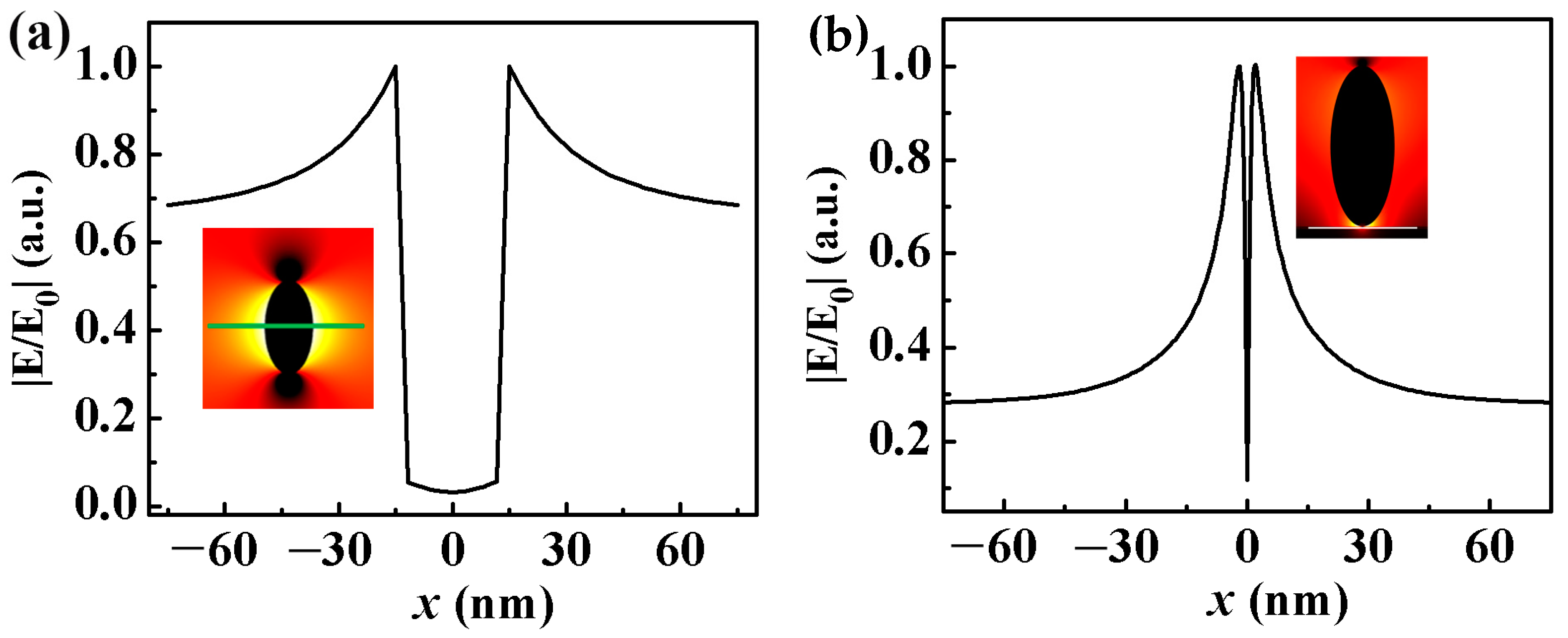
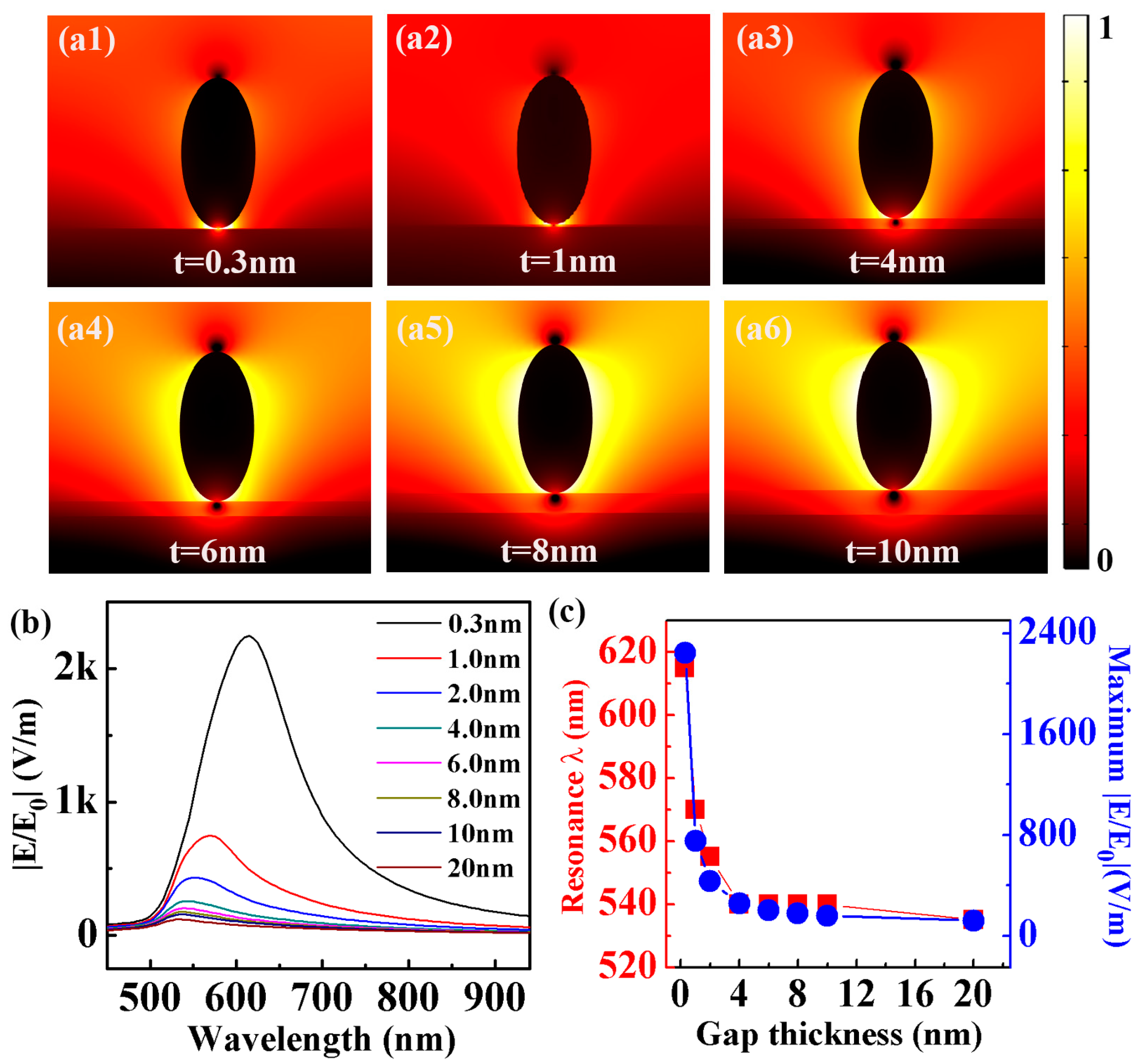
3.1. Electric Field Distribution on Surface of GNEPs and NPOM Structure

Under the excitation of incident light, the surface of the MNPs forms a local electric field. Similarly, there is a local electric field in the gap region of the NPOM structure composed of MNPs and thin films. But their structures are different, so there must be some differences in the electric field distribution. We want to see clearly the electric field distribution between them, so we select the position coordinates of the surface of the GENPs (Figure 2a, green line) and the interior of the gap of the NPOM structure (Figure 2b, white line) and extract the electric field intensity E/E0 for each coordinate position. As shown in Figure 2a, the position coordinates of the surface of the GENPs are normalized. The results show that the electric field intensity on the surface of the GENPs is the largest, and the electric field intensity gets smaller and smaller in the space far from the surface of the GENPs. As can be seen from the figure, at a distance of 60 nm from the surface of the GENPs, the electric field strength is only 30%. Therefore, when using MNPs for electric field enhancement applications, control of the MNP surface distance is very important. The normalized electric field values in the NPOM structure gap (along the white line) composed of GENPs and gold thin films are shown in Figure 2b. We can see from Figure 2b that the electric field intensity in the gap region is the largest, but the electric field intensity in the central position is minimized. There is a pole in the central position. Then, the electric field intensity decreases, and the decrease is much larger than that on the surface of the GENPs. At a distance from the center of 30 nm, the electric field strength decays by 70%. Finally, with the increase in the distance from the gap, the electric field intensity tends to be stable. We can also see their electric field distribution from the illustrations in Figure 2a,b. Compared with the GENPs, the local electric field of NPOM structure is mainly concentrated in the gap region. Next, we will systematically study the optical enhancement properties in the gap region of the NPOM structure.

3.2. Electric Field Distribution of NPOM Structure with Dielectric Layer with Thickness of 0.3 nm

Under the action of the coupling effect, the local electric field intensity in the gap region of the NPOM structure is much larger than that on the surface of single MNPs. The main factors affecting the local electric field intensity in the gap region of the NPOM structure are the polarization angle of the incident light, the thickness of the dielectric layer between the MNPs and the film, the material of the dielectric layer, the morphology of the MNPs and so on. The polarization angle of the incident light is a very important parameter. The resonance peak wavelength and the value of electric field in the gap region can be adjusted by changing the polarization angle. As shown in Figure 3, we keep the thickness of the dielectric layer at 0.3 nm and the refractive index of the dielectric layer at 1.36. The effects of six different polarization angles of incident light (0°, 15°, 30°, 45°, 60° and 75°) on the electric field value in the gap region are simulated systematically. As shown in Figure 3(a1–a6), the surface electric field distribution of the GENPs under different incident light polarization angles is shown. The results show that when the polarization angle is 0°, the electric field is mainly localized in the gap region and is symmetrically distributed. When the polarization angle increases to 15°, although the electric field is still localized in the gap region, it can be seen that the electric field is asymmetrically distributed. Then, as the polarization angle continues to increase, the electric field is more distributed on the surface of the GENPs, not just confined to the interior of the gap region. As shown in Figure 3(a5), when the polarization angle increases to 60°, a weak electric field distribution appears on top of the GENPs. In Figure 3(a6), we can clearly see a strong local electric field distributed on top of the GENPs (polarization angle of 75°).
In order to quantitatively obtain the variation in the electric field value with the polarization angle in the gap region of the NPOM structure, we further calculate the resonance spectrum of the electric field in the gap region (Figure 3b). The results show that the value of the electric field intensity decreases with the increase in the polarization angle. At the same time, the wavelength of the resonance peak shows a redshift with the increase in the polarization angle. In order to more intuitively see the change in resonance peak intensity and wavelength with the increase in the polarization angle, we process the resonance peak intensity and wavelength position of the resonance spectrum in Figure 3b, as shown in Figure 3c. It can be seen from the figure that when the polarization angle is small, the wavelength of the resonance peak rapidly red-shifts with the increase in the angle. With the increase in the polarization angle, the change trend of resonant wavelength becomes smaller and smaller. When the polarization angle increases from 60° to 70°, the wavelength corresponding to the peak of the resonance spectrum has almost no redshift. However, the relationship between the maximum electric field in the resonance spectrum and the polarization angle of the excitation light source is opposite. When the polarization angle is small, the electric field intensity of the resonance peak changes little with the increase in the polarization angle. With the increase in polarization angle, the electric field intensity of the resonance peak begins to decrease rapidly. The electric field intensity of the resonance peak corresponding to the polarization angle of 60° is about 1550 V/m, but when the polarization angle increases to 75°, the electric field intensity of the resonance peak decreases to 1125 V/m. The results show that the resonance peak intensity and wavelength of the electric field in the gap region of the NPOM structure can be accurately adjusted by changing the polarization angle of incident light.

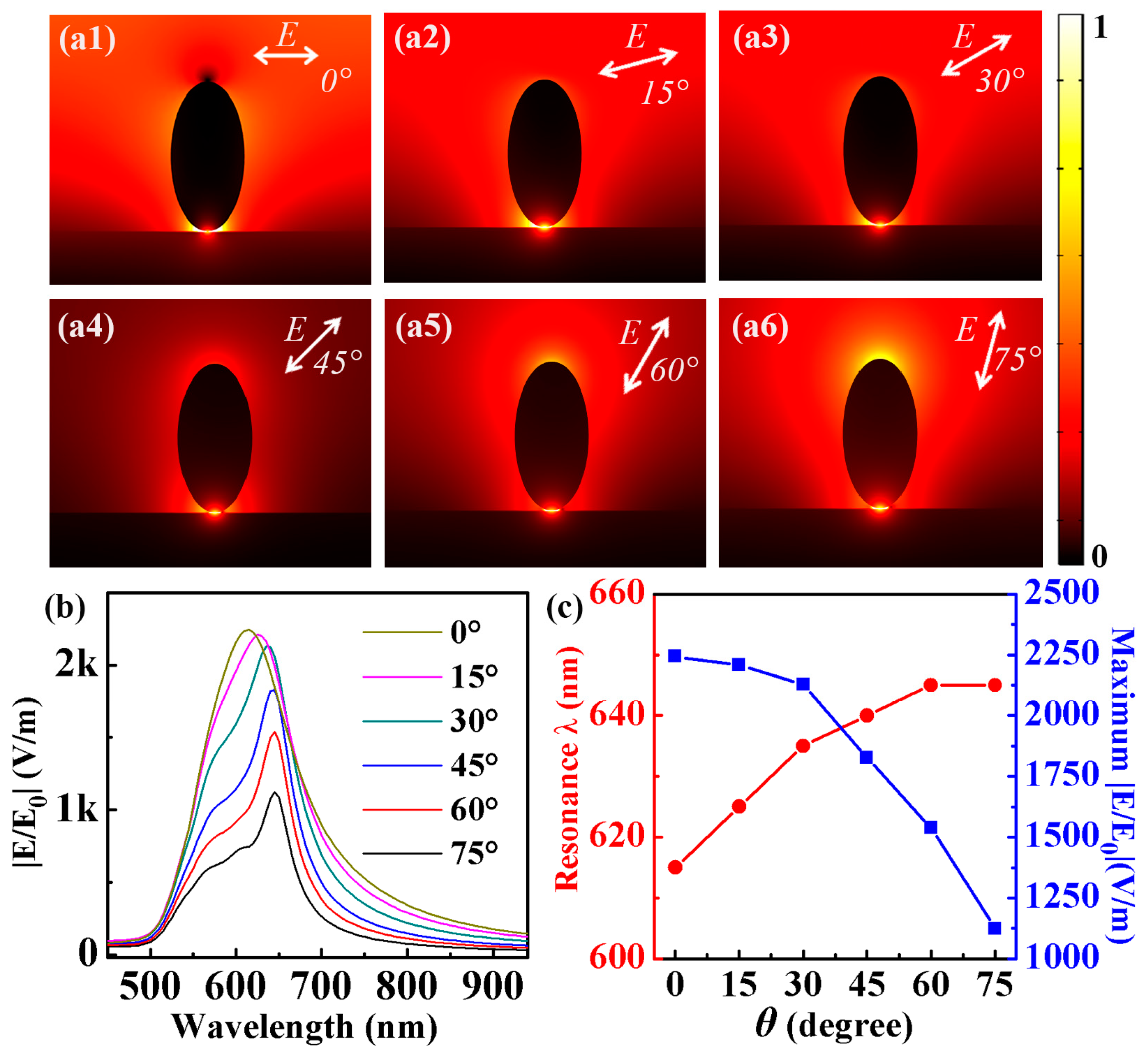
3.3. Electric Field Distribution of NPOM Structure with Dielectric Layer with Thickness of 1 nm

The polarization angle of incident light has an important influence on the resonance peak intensity and wavelength of the local electric field in the gap region of the NPOM structure. In addition, the peak value and wavelength position of the resonant field spectrum in the gap region are also affected by the thickness of the dielectric layer between the MNPs and the gold film. We set the thickness of the dielectric layer to 0.3 nm in Figure 3. With the other conditions remaining the same, the thickness of the dielectric layer is set to 1 nm, and the effect of the polarization angle on the electric field distribution in the bandgap region is studied. The results are shown in Figure 4(a1–a6). When the polarization angle is 0°, the electric field intensity is mainly localized in the gap region and still shows a symmetrical distribution. With the increase in the polarization angle, the local electric field in the gap region appears to have an asymmetrical distribution, but the electric field is still localized in the gap region. When the polarization angle increases to 60°, the electric field in the NPOM structure is no longer confined to the interior of the gap. As the polarization angle continues to increase to 75°, we see an obvious local electric field on top of the GENPs. The distribution of the local electric field on the surface of the NPOM structure is similar to that when the thickness of the dielectric layer is 0.3 nm. However, for the specific numerical changes, it is also necessary to process the data of the electric field distribution map, and the result is shown in Figure 4b. In Figure 4b, we see the same trend as in Figure 3b. The electric field intensity in the gap decreases with the increase in the polarization angle of the excitation light source. The wavelength of the resonance peak is red-shifted with the increase in the polarization angle. However, the intensity and wavelength of the resonance peak change obviously. As shown in Figure 4c, when the polarization angle is 0°, the intensity and wavelength of the local electric field resonance peak are 800 V/m and 570 nm, respectively. When the thickness of the dielectric layer is 0.3 nm, we can see from Figure 3c that the intensity and wavelength of the corresponding local electric field resonance peak are 2250 V/m and 615 nm, respectively. Similarly, it can be found from Figure 4c that the smaller the polarization angle is, the more obviously the wavelength of the resonance peak changes with the angle. With the increase in the polarization angle, the change in resonant wavelength is no longer significant. On the contrary, with a larger polarization angle, the peak value of the resonant field spectrum changes more significantly with the polarization angle of the excitation light source. However, if the polarization angle is small, the peak value of the electric field resonance spectrum no longer changes obviously with the increase in the polarization angle.

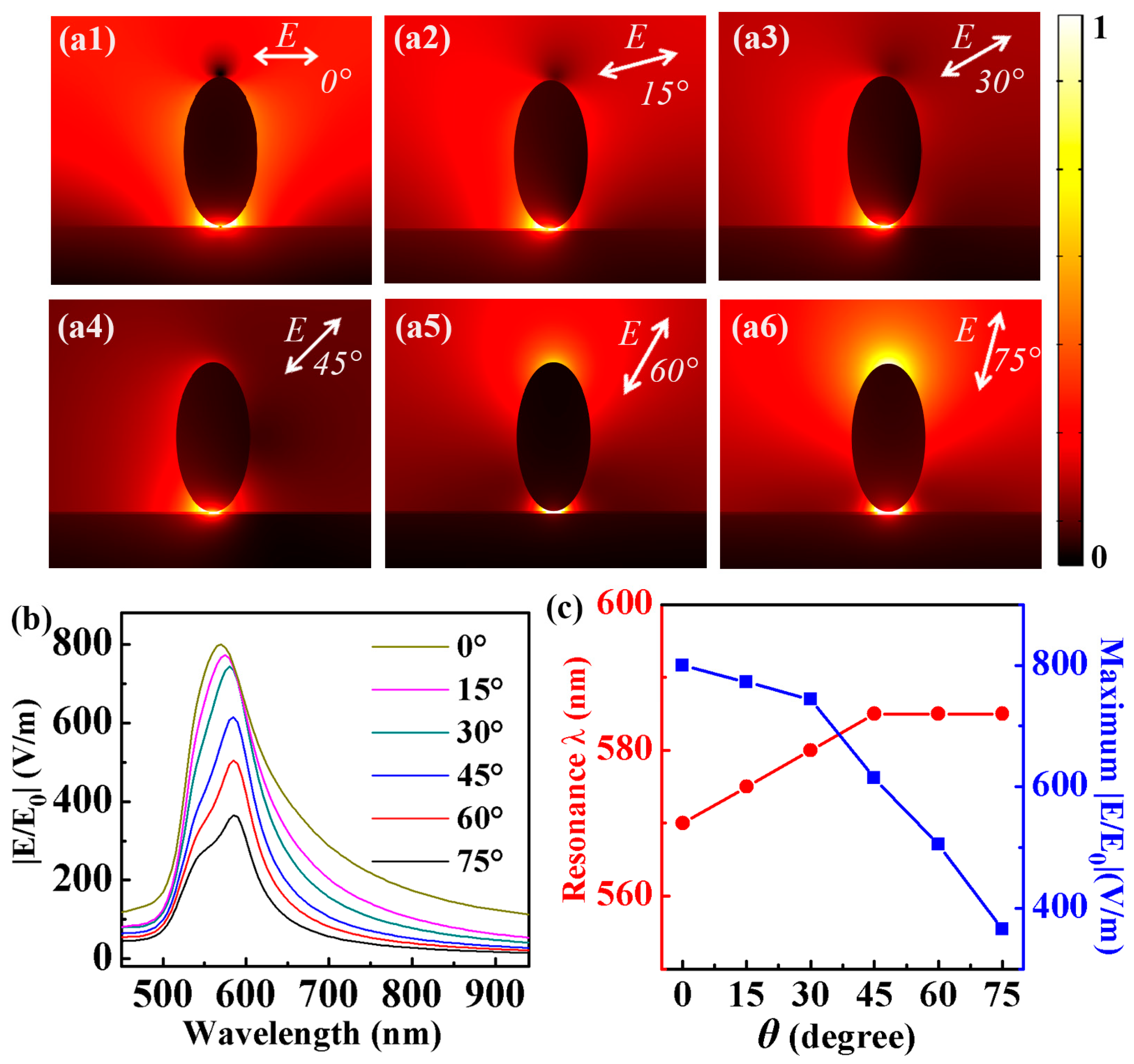
3.4. Electric Field Distribution of NPOM Structure with Dielectric Layer with Thickness of 4 nm

The intensity of the local electric field in the gap region of the NPOM structure is mainly affected by the coupling effect between the MNPs and the gold thin films. If the thickness of the dielectric layer is less than 2 nm, the coupling effect is strong. With the increase in the thickness of the dielectric layer, the coupling effect decreases gradually. We further set the thickness of the dielectric material between the gold nanoparticles and the gold thin films to 4 nm while keeping the other conditions unchanged. The electric field distribution of the NPOM structure at different polarization angles is shown in Figure 5(a1–a6). The results of Figure 5(a1) show that the surface electric field is no longer localized in the gap even when the polarization angle is 0° but also show a weak electric field distribution on the surface of the GENPs. When the polarization angle increases to 15°, this situation is more obvious, and the electric field is mainly localized on the left side of the GENPs. When the polarization angle increases to 60°, the electric field begins to appear on top of the GENPs. When the polarization angle is 75°, a clear electric field distribution can be seen on top of the GENPs. The results show that with the increase in the thickness of the dielectric layer, the electric field appears on the surface of the GENPs. As shown in Figure 5b, we quantitatively calculate the local electric field intensity spectrum in the electric field distribution figure. It can be found in the figure that the variation in the resonance intensity of the local electric field in the gap region remains the same as that in Figure 3b and Figure 4b. However, the change in the resonant wavelength of the electric field is obviously different. In order to see these changes more intuitively, we perform further data processing in Figure 5b (as shown in Figure 5c). We can see more clearly from Figure 5c that when the polarization angle is greater than 15°, the local electric field resonance wavelength does not change. However, the electric field intensity in the resonance spectrum still decreases rapidly with the increase in the polarization angle of the excitation light source. What is more important is that the peak value and wavelength position of the electric field resonance spectrum change obviously at the same polarization angle. Corresponding to the case of the polarization angle of 0°, the peak value of the electric field resonance spectrum is reduced to 275 V/m, and the resonant wavelength is 540 nm. From the above analysis, it can be concluded that the thickness of the dielectric layer can also control the intensity and wavelength of the local electric field resonance peak in the gap region.

3.5. Electric Field Distribution of NPOM Structure at Polarization Angle of 0°

From Figure 3, Figure 4 and Figure 5, the variation in electric field intensity in the gap region of the NPOM structure is studied when the thickness of dielectric layer is 0.3 nm, 1 nm and 4 nm, respectively. Through comparative analysis, it is found that the thickness of the dielectric layer has an important influence on the resonant peak intensity and wavelength of the electric field in the gap region. Under the condition of the same polarization angle of 0°, the intensities of the resonance peak are 2250 V/m, 800 V/m and 275 V/m, respectively. The resonant peak wavelengths are 615 nm, 570 nm and 540 nm, respectively. Therefore, we can also accurately adjust the resonance peak intensity and wavelength of the electric field in the gap region by changing the thickness of the dielectric layer. Then, we systematically study the relationship between the electric field in the gap region and the thickness of eight kinds of dielectric layers (0.3 nm, 1 nm, 2 nm, 4 nm, 6 nm, 8 nm, 10 nm and 20 nm). The surface electric field distributions of the NPOM structure with six kinds of dielectric layer thickness are shown in Figure 6(a1–a6). The results in Figure 6(a1) show that the electric field is mainly confined to the gap of the NPOM structure. With the increase in the thickness of the dielectric layer, the distribution of the electric field changes obviously. As shown in Figure 6(a4), when the thickness of the dielectric layer is 6 nm, there is an obvious electric field distribution on the surface of the GNEPs. With the increase in the thickness of the dielectric layer, this situation becomes more and more obvious. On this basis, we calculate the variation in the electric field in the NPOM structure with the thickness of the dielectric layer, as shown in Figure 6b. The results of the resonance spectrum show that the value of the electric field in the gap is inversely proportional to the thickness of the dielectric layer. And the smaller the thickness of the dielectric layer is, the more obvious the change is. However, the resonance peak wavelength of the electric field in the gap region has a blueshift with the increase in the thickness of the dielectric layer. Similarly, it can be seen that when the thickness of the dielectric layer is small, the change in the wavelength is more obvious. In order to see these changes more intuitively, we process the data in Figure 6b. The relationship between the resonant peak intensity and wavelength of the electric field in the gap region and the thickness of the dielectric layer is shown in Figure 6c. When the thickness of the dielectric layer is smaller than 4 nm, the intensity and wavelength of the electric field resonance peak have an obvious change trend. When the thickness of the dielectric layer exceeds 4 nm, the intensity and wavelength of the electric field resonance peak tend to be stable, and the range of change is very small. Therefore, only when the thickness of the dielectric layer is small, it is more meaningful to regulate the local electric field intensity in the NPOM structure.

4. Conclusions

The NPOM structure composed of GNEPs and gold thin films is simulated theoretically by the finite element method. The effects of the polarization angle of the incident light and the thickness of the dielectric layer on the electric field of the NPOM structure are studied systematically. The results show that the intensity of the local electric field in the gap region of the NPOM structure decreases with the increase in the polarization angle, while the wavelength position of the electric field resonance peak is red-shifted with the increase in the polarization angle of the excitation light source. At a smaller polarization angle, the redshift of the wavelength corresponding to the resonance peak is more significant with the increase in the polarization angle. But for the intensity of the resonance peak, the larger the polarization angle is, the more obvious the change is. Therefore, the resonance peak intensity and wavelength of the electric field in the gap region of an NPOM structure can be accurately adjusted by changing the polarization angle of the incident light. Finally, we also study the relationship between the thickness of the dielectric layer and the local electric field intensity in the gap region of the NPOM structure. The results of the resonance spectra show that the electric field intensity in the gap is inversely proportional to the thickness of the dielectric material. When the thickness of the dielectric layer is smaller than that of 4 nm, the electric field intensity in the gap region has a significant change trend. At the same time, the resonance peak wavelength of the electric field intensity in the gap region has a blueshift with the increase in the thickness of the dielectric layer. Similarly, when the thickness of the dielectric layer is small, the change in wavelength is more obvious. When the thickness of the dielectric layer exceeds 4 nm, the resonance peak wavelength remains stable. The proposed NPOM structure based on GNEPs and gold thin films has potential applications in the fields of SERS, optical gain, catalysis and so on.

Supplementary Materials

The following supporting information can be downloaded at: https://www.mdpi.com/article/10.3390/coatings14060746/s1, Figure S1: (a) Absorption spectra of gold spherical nanoparticles measured by experiments. (b) Resonance spectra of gold spherical nanoparticles simulated based on manuscript model.

Author Contributions

F.S. planned and guided the simulation study; Y.Z. constructed the simulation model; the manuscript was written by J.H. All authors have read and agreed to the published version of the manuscript.

Funding

This research was funded by Funding Scheme for Key Scientific Research Projects in Universities of Henan Province (grant No. 22A140024).

Institutional Review Board Statement

Not applicable.

Informed Consent Statement

Not applicable.

Data Availability Statement

Raw data are available from the corresponding author upon request.

Conflicts of Interest

The authors declare no conflicts of interest.

Nomenclature

AbbreviationDefinition
SERSsurface-enhanced Raman scattering
GENPsgold ellipsoidal nanoparticles
MNPsmetal nanoparticles
NPOMnanoparticle on mirror

References

  1. Yanglin, Z.; Kaiwen, Z.; Jinyan, N.; Tao, X.; Shenghao, W. Plasmonics in Organic Solar Cells: Toward Versatile Applications. ACS Appl. Electron. Mater. 2023, 5, 631–641. [Google Scholar]
  2. Bipasha, B.; Pekham, C.; Najirul, H.; Swarbhanu, G.; Mitali, S.; Aslam, K.; Manirul, I. AgNPs Embedded in Porous Polymeric Framework: A Reusable Catalytic System for the Synthesis of α-Alkylidene Cyclic Carbonates and Oxazolidinones via Chemical Fixation of CO2. Catalysts 2023, 13, 1467. [Google Scholar] [CrossRef]
  3. Shan, F.; Zhang, X.Y.; Fu, X.C.; Zhang, L.J.; Su, D.; Wang, S.J.; Wu, J.Y.; Zhang, T. Investigation of simultaneously existed Raman scattering enhancement and inhibiting fuorescence using surface modifed gold nanostars as SERS probes. Sci. Rep. 2017, 7, 6813. [Google Scholar] [CrossRef] [PubMed]
  4. Battulga, M.; Johannes, Z.; Hannes, P.; Christian, W.; Dmitry, S.; Markus, C.S.; Thomas, A.K.; Calin, H. Hybrid Multilayered Plasmonic Nanostars for Coherent Random Lasing. J. Phys. Chem. C 2016, 120, 23707–23715. [Google Scholar]
  5. Yeshchenko, O.A.; Bondarchuk, I.S.; Malynych, S.Z.; Galabura, Y.; Chumanov, G.; Luzinov, I. Surface plasmon modes of sandwich-like metal–dielectric nanostructures. Plasmonics 2015, 12, 655–665. [Google Scholar] [CrossRef]
  6. Shan, F.; Zhang, X.Y.; Wu, J.Y.; Zhang, T. Hot spots enriched plasmonic nanostructure-induced random lasing of quantum dots thin film. Chin. Phys. B 2018, 27, 047804. [Google Scholar] [CrossRef]
  7. Armstrong, R.E.; Liempt, J.C.; Zijlstra, P. Effect of film thickness on the far- and near-field optical response of nanoparticle-on-film systems. J. Phys. Chem. C 2019, 123, 25801–25808. [Google Scholar] [CrossRef]
  8. Zhu, S.Q.; Zhang, T.; Guo, X.L.; Zhang, X.Y. Self-assembly of large-scale gold nanoparticle arrays and their application in SERS. Nanoscale Res. Lett. 2014, 9, 114. [Google Scholar] [CrossRef] [PubMed]
  9. Hu, P.; Zheng, L.; Zhan, L.; Li, J.; Zhen, S.; Liu, H.; Luo, L.; Xiao, G.; Huang, C. Metal-enhanced fluorescence of nano-core–shell structure used for sensitive detection of prion protein with a dual-aptamer strategy. Anal. Chim. Acta 2013, 787, 239–245. [Google Scholar] [CrossRef]
  10. Hiroyuki, N.; Akito, M.; Sadahiro, M.; Tsunenobu, O.; Hitoshi, K.; Hidetoshi, O. Highly Controlled Plasmonic Emission Enhancement from MetalSemiconductor Quantum Dot Complex Nanostructures. J. Phys. Chem. C 2013, 117, 2455–2459. [Google Scholar]
  11. Jiang, N.; Zhuo, X.; Wang, J. Active Plasmonics: Principles, Structures, and Applications. Chem. Rev. 2018, 118, 3054–3059. [Google Scholar] [CrossRef] [PubMed]
  12. Nielsen, M.G.; Bozhevolnyi, S.I. Highly confined gap surface plasmon modes in metal strip-gap-film configurations. J. Opt. Soc. Am. B 2015, 32, 462–467. [Google Scholar] [CrossRef]
  13. Kim, M.; Lee, J.; Nam, J. Plasmonic photothermal nanoparticles for biomedical applications. Adv. Sci. 2019, 6, 1900471. [Google Scholar] [CrossRef] [PubMed]
  14. Langer, J.; Jimenez de Aberasturi, D.; Aizpurua, J.; Alvarez-Puebla, R.A.; Auguié, B.; Baumberg, J.J.; Bazan, G.C.; Bell, S.E.; Boisen, A.; Brolo, A.G.; et al. Present and future of surface-enhanced Raman scattering. ACS Nano 2020, 14, 28–117. [Google Scholar] [CrossRef] [PubMed]
  15. Ratchford, D.C. Plasmon-induced charge transfer: Challenges and outlook. ACS Nano 2019, 13, 13610–13614. [Google Scholar] [CrossRef] [PubMed]
  16. Kim, W.; Kim, N.; Park, J.W.; Kim, Z.H. Nanostar probes for tip-enhanced spectroscopy. Nanoscale 2016, 8, 987–994. [Google Scholar] [CrossRef] [PubMed]
  17. Guo, Q.; Ma, X.; Xie, Y.; Tan, W.; Zhang, H. Green synthesis and formation mechanism of Ag nanofowers using lcysteine and the assessment of Ag nanofowers as SERS substrates. Colloids Surf. A 2017, 530, 53–57. [Google Scholar]
  18. Khurana, K.; Jaggi, N. Localized surface plasmonic properties of Au and Ag nanoparticles for sensors: A review. Plasmonics 2021, 16, 981–999. [Google Scholar] [CrossRef]
  19. Vasanthan, D.; Jong, K.L.; Jin, W.O. Distinguishable Plasmonic Nanoparticle and Gap Mode Properties in a Silver Nanoparticle on a Gold Film System Using Three-Dimensional FDTD Simulations. Nanomaterials 2018, 8, 582. [Google Scholar] [CrossRef]
  20. Tanya, H.; Stephen, R.E.; Sumeet, M. Interaction of metallic nanoparticles with dielectric substrates: Effect of optical constants. Nanotechnology 2013, 24, 035201. [Google Scholar]
  21. Médéric, L.; David, M.; Priyamvada, V.; Gillibert, R.; Boujday, S.; Knoll, W.; Dostalek, J.; Chapelle, M.L. Plasmonic Properties of Gold Nanostructures on Gold Film. Plasmonics 2020, 15, 1653–1660. [Google Scholar]
  22. Vasanthan, D.; Hyun, L.; Minjun, K.; Thanh, M.N.; Jong, P.S.; Jong, M.L.; Lee, D.; Kim, K.H.; Oh, J.W. Unveiling facet effects in metallic nanoparticles to design an efficient plasmonic nanostructure. Curr. Appl. Phys. 2022, 44, 22–28. [Google Scholar]
  23. Jubb, K.M.; Jiao, Y.; Eres, G.; Retterer, S.T.; Gu, B. Elevated gold ellipse nanoantenna dimers as sensitive and tunable surface enhanced Raman spectroscopy substrates. Nanoscale 2016, 8, 5641–5648. [Google Scholar] [CrossRef] [PubMed]
  24. Near, R.; Tabor, C.; Duan, J.; Pachter, R.; El-Sayed, M. Pronounced effects of anisotropy on plasmonic properties of nanorings fabricated by electron beam lithography. Nano Lett. 2012, 12, 2158–2164. [Google Scholar] [CrossRef] [PubMed]
  25. Hatab, N.A.; Hsueh, C.H.; Gaddis, A.L.; Retterer, S.T.; Li, J.H.; Eres, G.; Zhang, Z.; Gu, B. Freestanding optical gold bowtie nanoantenna with variable gap size for enhanced Raman spectroscopy. Nano Lett. 2010, 10, 4952. [Google Scholar] [CrossRef] [PubMed]
  26. Liberman, V.; Adato, R.; Mertiri, A.; Yanik, A.A.; Chen, K.; Jeys, T.H.; Erramilli, S.; Altug, H. Angle-and polarization-dependent collective excitation of plasmonic nanoarrays for surface enhanced infrared spectroscopy. Opt. Express 2011, 19, 11202–11212. [Google Scholar] [CrossRef] [PubMed]
  27. Yeshchenko, O.A.; Tomchuk, A.V.; Kozachenko, V.V.; Knize, R.J.; Haftel, M.; Pinchuk, A.O. Angle and polarization dependent coupling of surface plasmon and gap modes in plasmonic gap metasurfaces. Opt. Mater. 2022, 132, 112884. [Google Scholar] [CrossRef]
  28. Jiang, M.; Wang, G.; Xu, W.; Ji, W.; Zou, N.; Ho, H.P.; Zhang, X. Two-dimensional arbitrary nano-manipulation on a plasmonic metasurface. Opt. Lett. 2018, 43, 1602–1605. [Google Scholar] [CrossRef] [PubMed]
  29. Palik, E.D. Handbook of Optical Constants of Solid; Academic Press: Orlando, FL, USA, 1985. [Google Scholar]
  30. Li, L.; Hutter, T.; Steiner, U.; Mahajan, S. Single molecule SERS and detection of biomolecules with a single gold nanoparticle on a mirror junction. Analyst 2013, 138, 4574–4578. [Google Scholar] [CrossRef]
  31. Sehmi, H.S.; Langbein, W.; Muljarov, E.A. Optimizing the Drude-Lorentz model for material permittivity: Method, program, and examples for gold, silver, and copper. Phys. Rev. B 2017, 95, 115444. [Google Scholar] [CrossRef]
Figure 1. (a) A schematic diagram of the NPOM structure separated by a dielectric layer. (b) The calculation model of the NPOM structure separated by a dielectric layer.
Coatings 14 00746 g001
Figure 2. (a) The normalized electric field on the surface of the GENPs (along the green line) in a homogeneous medium. (b) The normalized electric field value in the gap region of the NPOM structure (along the white line) composed of GENPs and gold thin films.
Coatings 14 00746 g002
Figure 3. (a1a6) Electric field distribution of NPOM structure at different polarization angles with dielectric layer with thickness of 0.3 nm. (b) Resonance spectrum curve of electric field intensity in gap region under different polarization angles. (c) Relationship between polarization angle and electric field intensity.
Coatings 14 00746 g003
Figure 4. (a1a6) Electric field distributions of NPOM structure with different polarization angles with dielectric layer with thickness of 1 nm. (b) Resonance spectrum curve of electric field in NPOM structure under different polarization angles. (c) Relationship between polarization angle and electric field intensity.
Coatings 14 00746 g004
Figure 5. (a1a6) Electric field distribution of NPOM structure with different polarization angles with dielectric layer with thickness of 4 nm. (b) Resonance spectrum curve of electric field intensity in gap region under different polarization angles. (c) Relationship between polarization angle and electric field intensity.
Coatings 14 00746 g005
Figure 6. (a1a6) Electric field distribution of NPOM structure with different thickness of dielectric layer at polarization angle of 0°. (b) Resonance spectrum curve of electric field intensity in gap region at different thickness of dielectric layer. (c) Relationship between thickness of dielectric layer and electric field intensity.
Coatings 14 00746 g006
Disclaimer/Publisher’s Note: The statements, opinions and data contained in all publications are solely those of the individual author(s) and contributor(s) and not of MDPI and/or the editor(s). MDPI and/or the editor(s) disclaim responsibility for any injury to people or property resulting from any ideas, methods, instructions or products referred to in the content.

