Article

The Effect of Deposition Temperature on TiN Thin Films for the Electrode Layer of 3D Capacitors Prepared by Atomic Layer Deposition

1
School of Microelectronics, Shanghai University, Shanghai 201800, China
2
CAS Key Laboratory of Inorganic Functional Materials and Devices, Shanghai Institute of Ceramics, Chinese Academy of Sciences, Shanghai 201899, China
3
College of Materials Science and Opto-Electronic Technology, University of Chinese Academy of Sciences, Beijing 100049, China
*
Authors to whom correspondence should be addressed.
Coatings 2024, 14(6), 724; https://doi.org/10.3390/coatings14060724
Submission received: 29 April 2024 / Revised: 27 May 2024 / Accepted: 3 June 2024 / Published: 5 June 2024
(This article belongs to the Special Issue Thin-Film Synthesis, Characterization and Properties)

Abstract

:
The TiN thin film is considered a promising electrode layer for 3D capacitors. In this study, TiN thin films were prepared on Si substrates using atomic layer deposition (ALD) at various temperatures from 375 °C to 475 °C. The crystallization behavior, microstructure, and conductance properties of those TiN thin films were investigated. The resistivity of TiN thin films deposited on Si wafers can reach as low as 128 μΩ·cm. TiN thin films showed lower resistivity and worse uniformity with the deposition temperature increasing. In addition, the aging of TiN thin films may weaken the device performance. Optimized deposition parameters were found and full-coverage deposition of thin films on the wall of deep holes with an aspect ratio of approximately 14 has been successfully achieved. The results would be a good reference for the development of 3D capacitors and other microelectronics components.

1. Introduction

The 3D silicon capacitors have gained much attention in recent years for their excellent high-frequency performance and wide working temperature window [1,2]. Unlike the traditional multi-layered ceramic capacitors (MLCCs) achieving high capacitance density by increasing the number of lamination layers and reducing the dielectric layer thickness, the 3D silicon capacitors obtain high capacitance density by increasing the effective area through etching the silicon substrate to form deep holes, grooves, nanopillars, or other 3D microstructures. The 3D capacitors with multi-layer thin films of the electrode layer/dielectric layer/electrode layer would be prepared as conformal with the 3D microstructure in the substrate [3,4]. The electrode layer of the 3D capacitors needs to have high conductivity and no chemical reaction with the dielectric layer. Furthermore, the material can be easily deposited into the deep holes or other 3D microstructures to form a conformal 3D electrode layer. Among many electrode materials, TiN thin films are an excellent choice.
TiN is a versatile hard ceramic material with wear resistance, corrosion resistance, and good electrical conductivity, rendering it a popular electrode choice for fuel cells, super capacitors [5,6,7], resistive random memory (RRAM) [8], resistive-switching devices [9], phase-change memory (PCM) [10], and numerous other electronic devices. Currently, various preparation techniques exist for the preparation of TiN thin films, including magnetron sputtering ion plating (MSIP) [11,12,13], arc ion plating (AIP) [14,15], chemical vapor deposition (CVD) [16,17], and electrostatic spray coating (ESC) [18]. Atomic layer deposition (ALD), as a special chemical vapor deposition (CVD) technology, has attracted researcher’s attention in the past few decades [19,20,21,22]. Because of its self-limiting and self-saturation characteristics, ALD can achieve accurate control of film thickness and composition. In particular, conformal thin films can be formed on the wall of deep holes and other irregular substrates by the ALD method [23,24]. There have been reports on preparing TiN thin films by the ALD method using different precursors on different substrates [25,26] but few reports on deposition TiN thin films on a silicon substrate with deep-hole arrays [27].
In this study, TiN thin films were prepared by ALD at various temperatures, to investigate the effect of deposition temperature on the conductance characteristics of TiN thin films. And, the characteristics of ALD TiN thin films on a silicon substrate with deep-hole arrays at various deposition temperatures were also presented and analyzed. These results should contribute to improving the performance of TiN thin films for 3D capacitor fabrication.

2. Experimental

2.1. Sample Preparation

TiN thin films were prepared using TiCl4 (Kemicro, Suzhou, China) and NH3 (Rauchon Chemical, Shanghai, China) as precursors using the TALD-100R-DL ALD system (Kemicro, Suzhou, China). Typical planar silicon wafers (>10 kΩ·cm, crystal orientation (100)) and a silicon wafer with deep-hole arrays were used as substrates. The substrates were cleaned sequentially with a solution of H2O2 (Sinopharm, Shanghai, China) and H2SO4 (1:3) (Sinopharm, Shanghai, China), HF (>40%) (Sinopharm, Shanghai, China), and acetone (Sinopharm, Shanghai, China), and then blow dried using N2 (Rauchon Chemical, Shanghai, China) gas (the SEM and AFM images of the cleaned wafers are shown in Figures S1 and S2). During the film deposition, an ALD cycle consisted of a 0.4 s pulse of the TiCl4 precursor, followed by another 20 s pulse of NH3. The N2 purge was introduced in between the pulses, to remove the excess precursors and reaction by-products. The purity of liquid nitrogen used in the experiment was 99.999%, and the purifier (Simpure, Shanghai, China) processed N2 purity up to 99.99999%. The ALD TiN process could be regarded as the combination of two half reactions between the TiCl4 precursor and NH3 gas, shown as Equations (1) and (2) [28]:
T i C l 4 + 2 H N 3 T i N + 4 H C l + H 2 + 1 2 N 2
6 T i C l 4 + 8 H N 3 6 T i N + 24 H C l + N 2
And, the initial stage of growth has been shown in Figure 1.

2.2. Sample Characterization

The thickness of TiN samples was measured by spectroscopic ellipsometry (SE, V-VASE, J.A. Woollam, Lincoln, NE, USA) with a spectral range of 0.8–5.2 eV per 0.2 eV (wavelength range of 238.5–1550 nm) at three incident angles of 65°, 70°, and 75°. The establishment of a proper model of the film structure and proper dispersion functions for the materials is a key step to fitting the measured ellipsometry parameters, psi and delta. The dielectric function of the TiN thin films can be modeled by a Drude–Lorentz oscillator parametrization and the ellipsometry data can be expressed in terms of the dielectric function Ɛ, which is represented in real Ɛ1 and imaginary Ɛ2 parts. The adopted Drude–Lorentz model consisted of a Drude term and 2 Lorentz oscillators could be described, as below (Equation (3)):
ε ω = ε ω p u 2 ω 2 i Γ D ω + j = 1 2 f j ω 0 j 2 ω 0 j 2 ω 2 + i γ j ω
Here, the Drude term is characterized by the un-screened plasma energy ħωpu and the damping factor ΓD, and the two Lorentz oscillators are located at energy position ħω0j, with strength ƒj and damping factor γj. Meanwhile, the Ɛ is equal to or larger than unity to compensate for the contribution of higher-energy transitions that are not taken into account by the Lorentz terms. The refractive index and extinction coefficient curves can be derived from a complex dielectric according to Equation (4) [29]:
ε 1 = n 2 + k 2 , ε 2 = 2 n k
Then, the thickness of the film would be analyzed and calculated by the software WVASE32 v3.736. It can be obtained perfectly from model fitting, which has been demonstrated in previous studies [30,31].
The resistivity of TiN samples was calculated from the square resistance measured by a Four-probe Tester (RTS-9, 4 Probes Tech, Guangzhou, China). The surface morphology of the film was obtained by Scanning Electron Microscope (FEI, Verios G4, Hillsboro, OR, USA; Hitachi, SU-9000, Tokyo, Japan). The crystallization of the films was analyzed by X-ray Diffraction (XRD, D8 DISCOVER, Bruker, Berlin, Germany) with Cu Kα in grazing incidence XRD scan mode at 40 kV and 200 mA. Atomic Force Microscopy (AFM, Ntegra Platform, NT-MDT, Moscow, Russia) was used to characterize the surface topography and roughness in tapping mode. The results were displayed and calculated by Gwyddion v2.43 software. The composition and element valence state of the samples were measured by X-ray Photoelectron Spectroscopy (ESCAlab250 Xi, Thermo Scientific, Waltham, MA, USA). The samples were aged by a High-Temperature High-Humidity Burn-in Test System (H3MKP2010, ATiS HangKe, Zhenjiang, China).

3. Result and Discussion

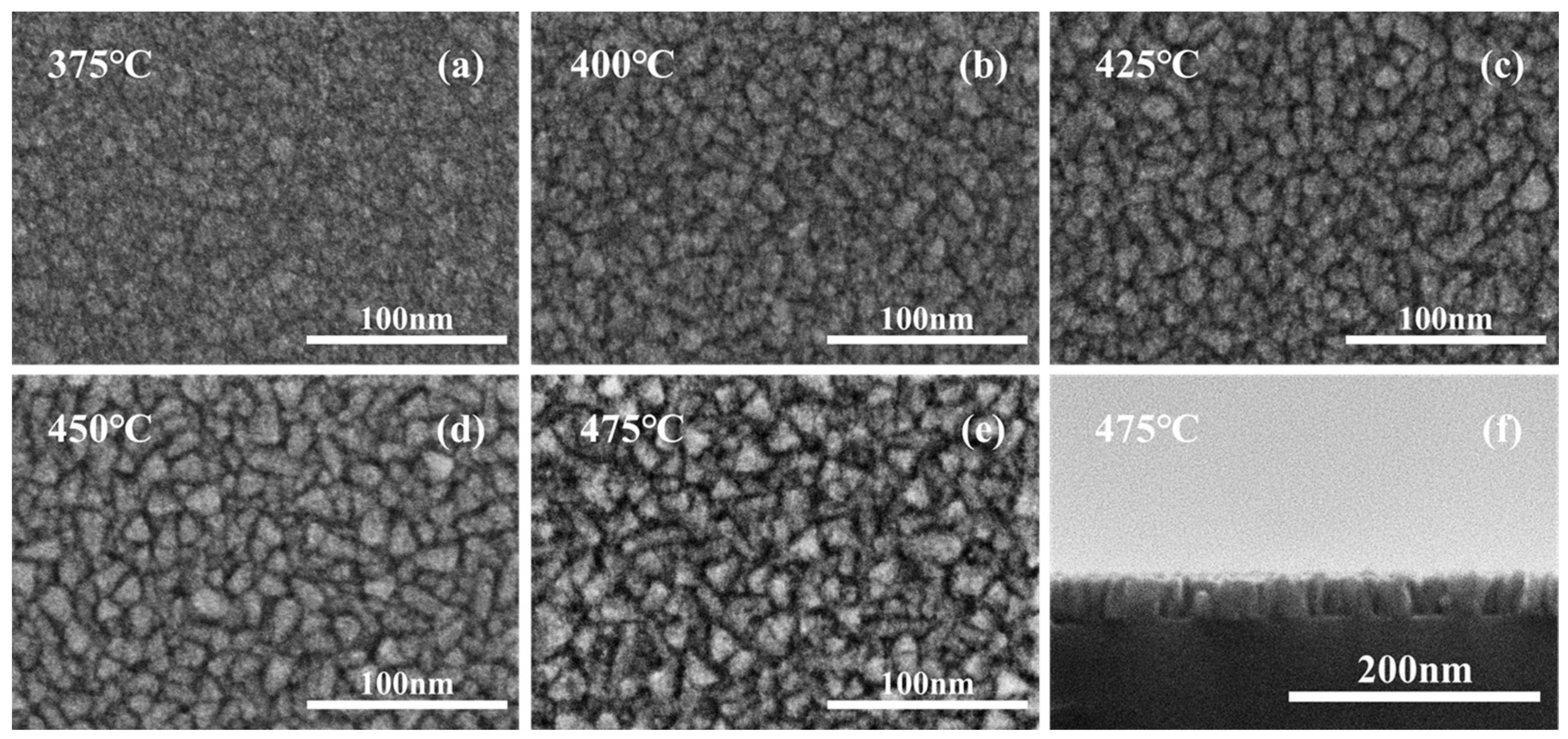
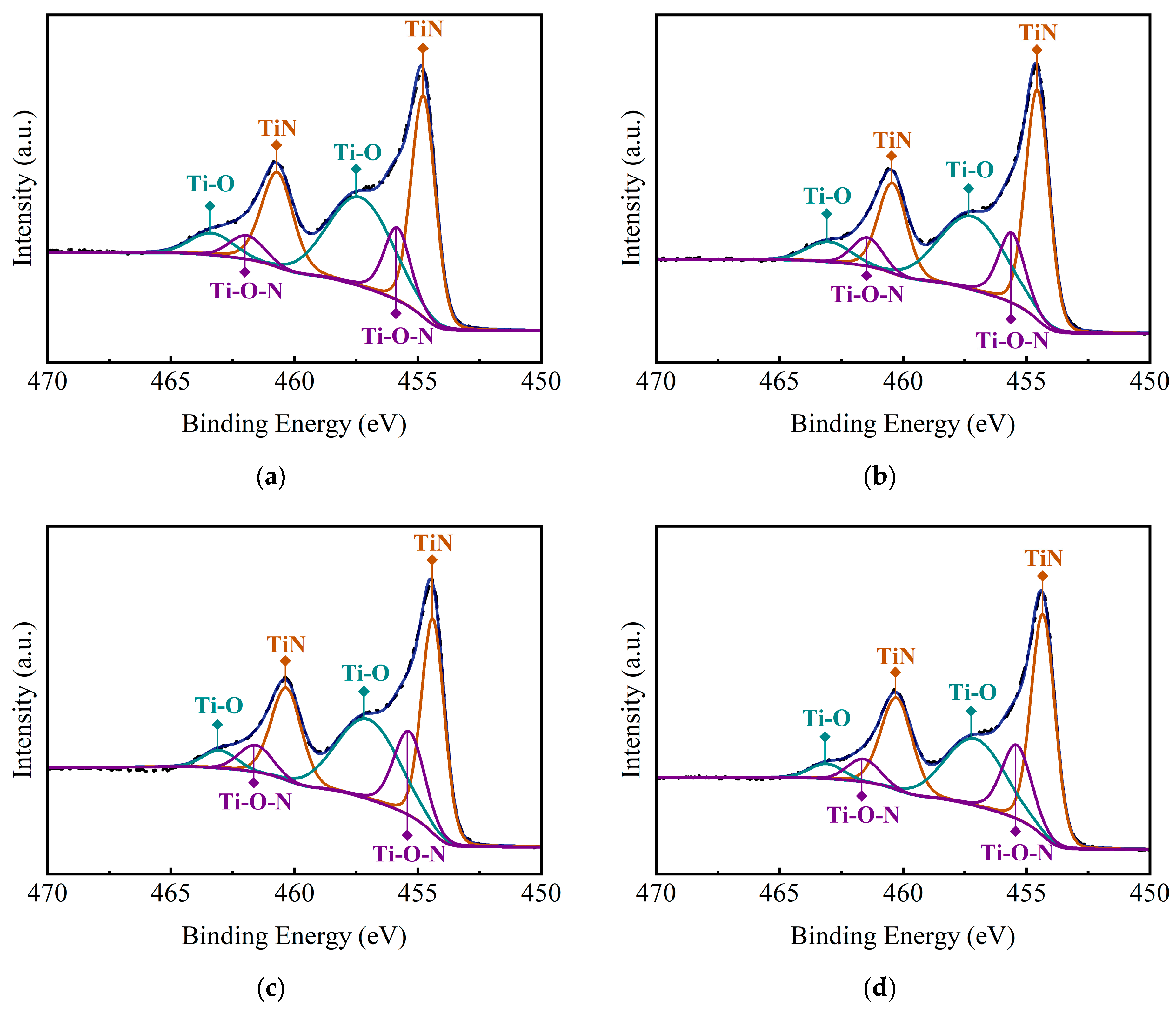
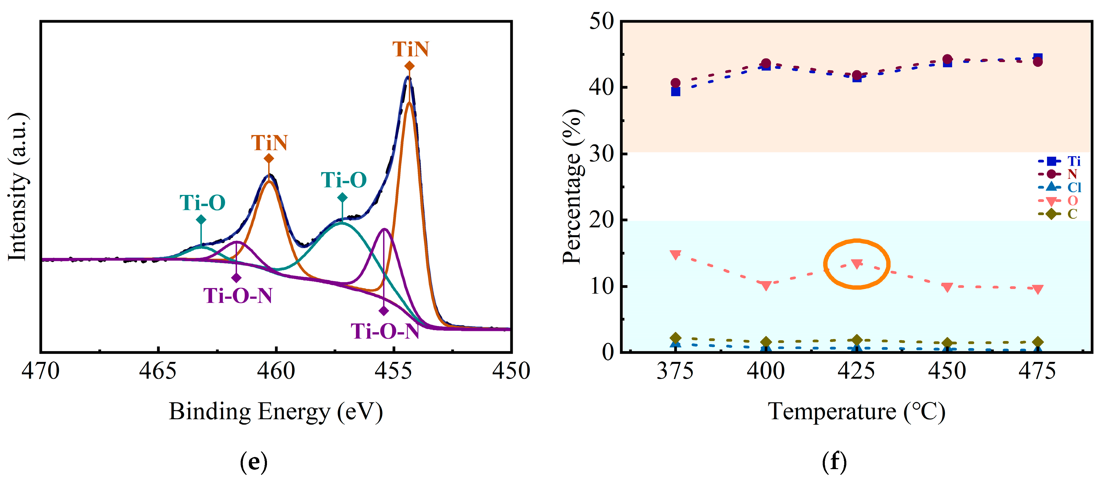
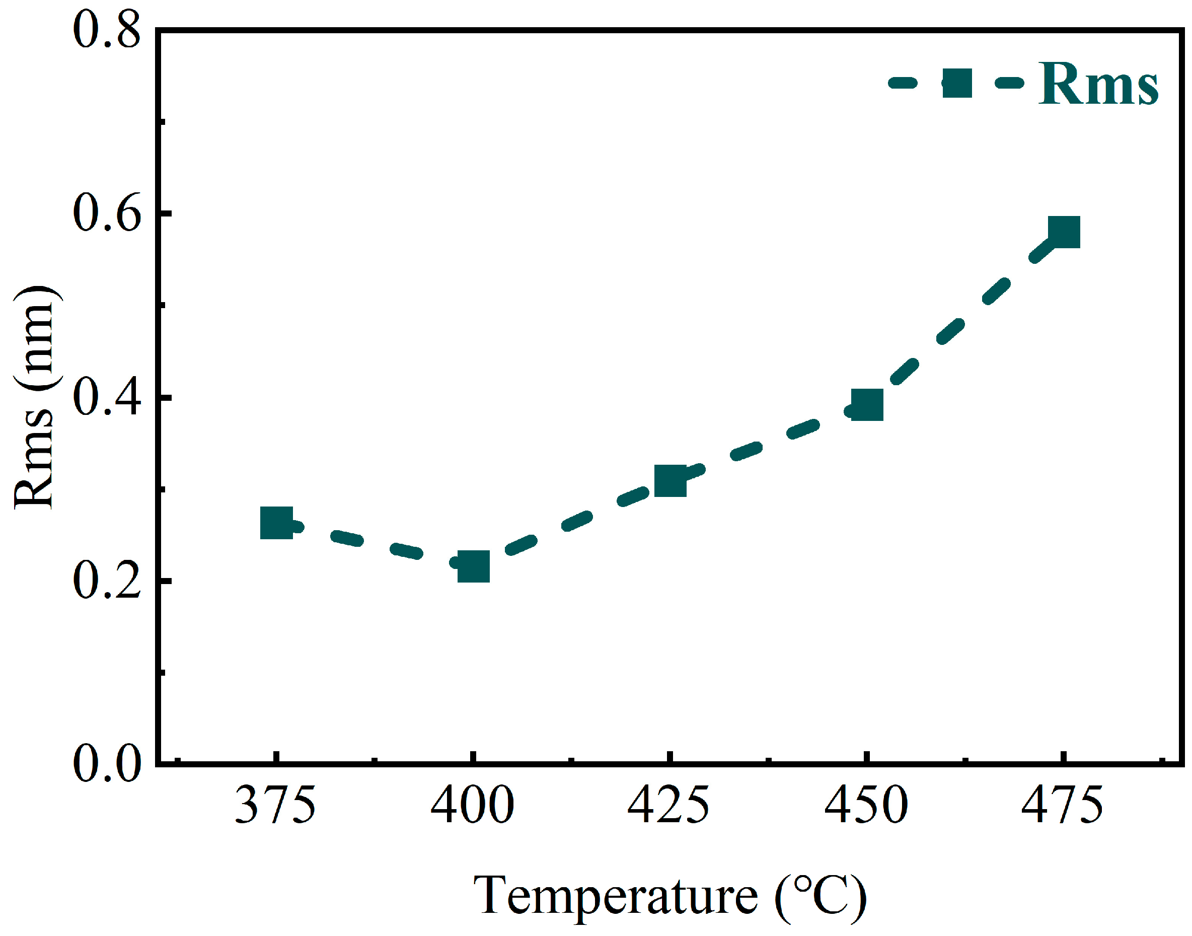
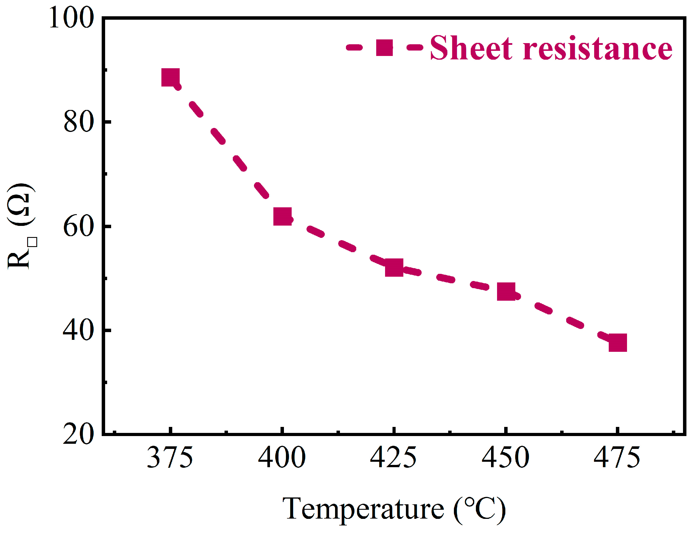
3.1. TiN Thin Films Deposited on Planar Substrates at Different Temperatures

The ALD temperature is closely related to the various properties of the prepared films. Understanding the effect of deposition temperature on the electrical properties of TiN thin films would be beneficial to obtaining high quality TiN thin films for the electrode layer of the 3D capacitors. For TiN-thin-film deposition, the substitution reaction between the TiCl4 precursor and NH3 reaction gas requires heating the substrate at a temperature to activate the self-limiting reaction. Thus, the same 1000-cycle TiN thin films were prepared at five different temperatures, 375 °C, 400 °C, 425 °C, 450 °C, and 475 °C, for each.
After depositing, variable-angle spectroscopic ellipsometry was used to measure the TiN thin films, followed by dispersion model fitting to obtain the film thickness to calculate the growth rate. It can be seen in Figure 2a that the growth per cycle (GPC) of TiN thin films has no obvious change up to 425 °C (the measurement principle and fitting results of spectroscopic ellipsometry are shown in Figures S3 and S4, and the discussion of measurement error has been described in detail). But, the GPC increases with the deposition temperature increase. Then, the resistivity of the samples was also calculated from the measured sheet resistance and thickness, shown in Figure 2b. Obviously, there is a remarkable decline in resistivity with the increase in the deposition temperature. And, a resistance as low as 128 μΩ·cm could be obtained at a deposition temperature of 475 °C.
In order to clarify how the deposition temperature affects the growth and conductance properties for TiN thin films, the GIXRD was taken to present the phase composition of TiN thin films with various deposition temperatures. The results of GIXRD analysis for TiN thin films confirmed that the films were polycrystalline (Figure 3). The TiN thin films show no preferred orientation at low deposition temperatures and preferred to grow along the (111) orientation at elevated deposition temperatures. It could be explained that the molecules would receive excess energy during the process of forming films with the increase in deposition temperature, which enhanced their diffusion ability on the substrate surface, and promoted the oriented crystallization of TiN thin films.
The SEM characterization of the morphology of the samples was shown in Figure 4a–f. It could be obviously seen that the crystallization degree of the low-temperature samples was much lower than that of the high-temperature samples, and plentiful and large crystalline grains of the 475 °C sample could be seen clearly in the cross-section characterization in Figure 4f as well. Compared with TiN thin films deposited at a high temperature, the grains of samples deposited at a lower temperature were obviously smaller and the grain boundaries were richer, worsening the scattering effect on the carrier, which resulted in the increasing resistivity of TiN thin films. Meanwhile, fewer grain boundaries would also result in fewer channels for oxygen to enter the film, reducing the oxygen content of TiN thin films, which could be confirmed by XPS results.
Figure 5 presents the XPS spectra and the atom contents of TiN samples deposited on planar Si substrates at different temperatures. There are two distinct peaks located at 455.1 eV and 460.7 eV, which can be observed from the spectra. The peaks are very close to the 454.2 eV and 460.3 eV documented in the literature and can be identified as corresponding to Ti2p3/2 and Ti2p1/2 due to Ti2p orbital splitting [32,33]. The XPS spectra can be well fitted into six peaks using Gaussian fitting, which are shown in Table 1. It could be found that the thin films are dominated by the Ti-N bond, and the content of N and Ti atoms rise higher with the increasing deposition temperatures. Meanwhile, the presence of Ti-O-N and Ti-O indicates the introduction of elemental O during the deposition process (the O1s energy spectra of the 375 °C samples were provided, shown in Figure S5). Since the carrier gas used liquid nitrogen after purifier treatment throughout the deposition process, it is inferred that the O element mainly comes from the impure precursors.
Furthermore, according to the previous XRD patterns, the diffraction peaks of TiO2 were not obtained. It is considered that the Ti-O bonds shown in the XPS spectra are due to the substitution of N atoms by O atoms in the TiN lattice, rather than in the form of TiO2 grains. Moreover, the insertion of O atoms into the Ti-N bonds also results in the formation of Ti-O-N bonds, in addition to the substitution phenomenon [34]. It is interesting to see that there is a small increase in O content at 425 °C, which is circled in Figure 5f. When the deposition temperature increased to 425 °C, the crystallization of TiN thin films transformed from polycrystalline into a columnar grain structure dominated by TiN (111) orientation. The microstructure change may result in a lower density of the TiN thin films and a small increase in O content [35].
Meanwhile, the XPS results could also be used to explain the optimization of the resistivity of the TiN thin films. The electrical conductivity of TiN thin films depends mainly on the bonding state between Np and Tid, which results from the hybridization of Ti and N atoms. The weak interaction force between free electrons in the TiN crystal structure is caused by the lower 2p orbital energy level of N atoms compared to the Fermi energy level. This allows the free electrons to move throughout the crystal structure and be shared by the entire structure. Therefore, the resistivity for TiN samples decreases as the quantity of Np-Tid bonding states increases with the increasing atom content for Ti and N. Although TiN thin films deposited at high temperatures have the advantage of high electrical conductivity, it is important to note that an increase in the degree of crystallization may lead to an increase in the roughness of the films [36]. Therefore, AFM characterization was performed on the films deposited at different deposition temperatures, as shown in Figure 6, and the root mean square of roughness was calculated by Gwyddion and is shown in Figure 7.
It can be seen that the overall roughness increases with the increase in deposition temperature, and it can also be seen from the AFM 3D images that the grains on the surface of the TiN films show an increase in number and combined growth. This is consistent with the XRD patterns, which indicated that the crystallization of the film after 425 °C is more and more uniform toward the formation of grains in the (111) direction. The effective crystallization and oriented growth of the TiN thin films at elevated temperatures lead to a significant increase in roughness. For films deposited by ALD, the increase in film roughness is bound to lead to instability in the film growth rate, which may affect the precise growth of film thickness [36].
Furthermore, the highest Rms value observed was 0.58 nm. ALD-prepared films typically exhibit superior surface roughness compared to other preparation methods [37,38]. The surface roughness obtained in this study was slightly better in TiN thin films deposited by ALD, which has been reported previously [39]. This may be due to the difference in annealing time and annealing temperature. Considering that TiN electrodes mainly play a role in 3D capacitors in terms of their electrical properties, TiN thin films with better electrical conductivity are more suitable for use as an electrode layer, which negates the side effect of a small amount of rising roughness. Therefore, the TiN thin films deposited at 475 °C would be more applicable for 3D capacitors.

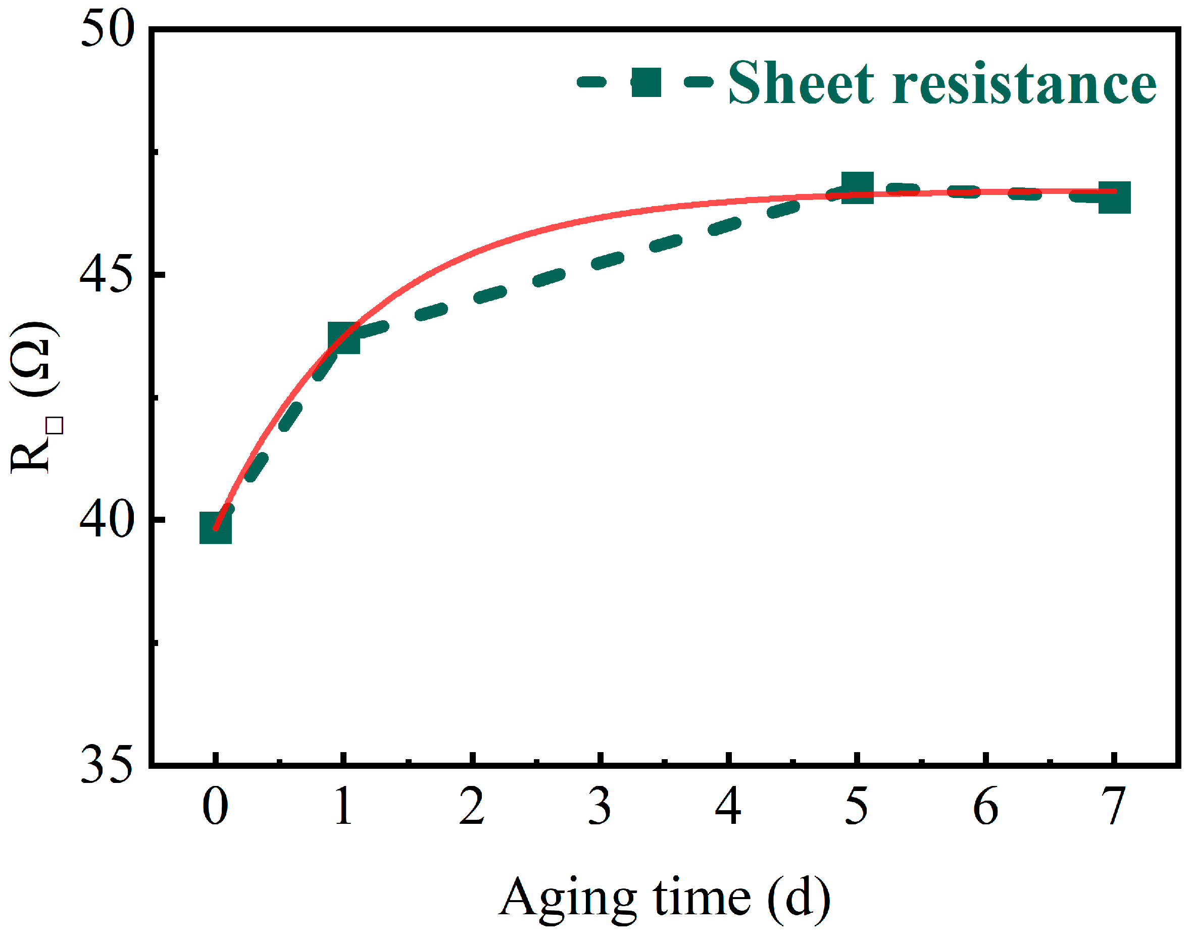
3.2. TiN-Film Aging Experiments

In order to investigate the changes in TiN thin films under conditions of elevated temperature and humidity, aging experiments were conducted for the application of 3D capacitors. The experiments were conducted by placing the TiN thin films in an environment set at 85 °C and 85% humidity. Samples of 1000-cycle TiN thin films were deposited at 475 °C and characterized after being placed for 0, 1, 5, and 7 days.
A four-probe square resistance test was performed on the sample first and the results are shown in Figure 8. It can be observed that the square resistance exhibits a slight increase with prolonged aging. And, the square resistance reaches approximately 46.7 Ω after 7 days of aging.
To explore the reason for the increase in the square resistance, the samples were characterized by XPS, and Figure 9a illustrates the elemental atom ratios within the films after etching the samples for 120 s. It is evident that the concentrations of Ti and N atoms in the film decrease gradually with increasing aging time, from an initial value of about 45% to a final value of about 30%. Concurrently, the oxygen atom content increases from 7% to 27%, indicating that the O element is introduced into the film in a hot and humid environment, which results in a reduction in the number of carriers present within the films. It is possible that oxygen elements may exist in the layer as TiO2 may replace the N atoms or form Ti-O-N bonds. Therefore, the Ti2p energy spectra of the samples after aging for seven days were analyzed, as shown in Figure 9b. It can be observed that the peak area of the Ti-N bond decreases from 53.2% to 35.7%, while the peak area of the Ti-O-N bond increases from 19.23% to 31.52%, in comparison with the previous section. That means the O element mainly existed as a Ti-O-N bond. Meanwhile, to confirm whether TiO2 grains appeared in the samples after 7 days of aging, the samples were subjected to XRD analysis (Figure 10). The results did not reveal the diffraction peaks of TiO2, and the scattering of the carriers would not be enhanced. Therefore, the square resistance of the aged sample does not increase significantly. The aging process indicates that with the extension of the service cycle, the aging and deterioration of the TiN thin films will affect the performance strength of the 3D capacitors.

3.3. TiN Thin Films Deposited on Substrates with Deep-Hole Arrays at Different Temperatures

To confirm whether similar properties can be exhibited on porous structures, TiN thin films were deposited at various temperatures on substrates with deep-hole arrays. The hole diameter was around 4.61 μm, hole depth was around 64.87 μm, and the pore spacing was around 3.33 μm. The prepared films were then characterized using a four-probe analysis, and the results are presented in Figure 11. The results show that the square resistance of TiN thin films deposited on deep-hole structures at different temperatures decreases significantly with increasing deposition temperature, which agrees with the planar results. And, the SEM characterization was also performed and the results are shown in Figure 12. It can be seen that the film can be deposited perfectly inside deep holes, on the top, the sidewall, and the bottom. This demonstrates the excellent conformality that is unique to the ALD process.
The thickness of the film was measured multiple times at three positions: the top, wall and bottom of the hole. The results are presented in Table 2. The data in the table were processed to obtain the variance of thickness at different locations and deposition temperatures. The thickness data of the three positions were averaged separately and then the variance formula (Equation (5)) was used to obtain the inhomogeneity of the film layers at different positions and temperatures.
V a r = x i x ¯ 2 n
where xi represents the average thickness at different locations, x ¯ represents the overall average thickness, and n is the number of samples (n = 3). The corresponding results are presented in Figure 13.
The decrease in film thickness uniformity with increasing deposition temperature is evident. This indicates that the temperature-dependent deposition characteristics of TiN thin films deposited on porous structures are similar to those of planar TiN thin films. This may affect the precise control of the thickness of the film deposited in the porous structure, which in turn, affects the performance of the prepared devices. Further studies will focus on improving the homogeneity of the multi-layers on the porous structure substrates, while completing the preparation and performance testing of the 3D capacitor prototype device.

4. Conclusions

In this study, TiN thin films were prepared using ALD. The temperature-dependent nature of the microstructure, surface morphology, and conductivity properties were analyzed. The conductivity of TiN thin films improved with the increase in deposition temperature. The TiN thin films deposited at high temperatures, both on planar and porous silicon substrates, have good electrical conductivity. TiN films have a low resistivity of around 128 μΩ·cm at 475 °C. In addition, the degree of crystallinity of TiN films increases with increasing temperature, and the crystallographic orientation shifts towards (111) with increasing temperature. Meanwhile, after 7 days aging in the high-heat and high-humidity environment, the electrical properties of TiN thin films were weakened due to the increasing O content up to 27%. The morphology of O elements inside the films of the aged samples was also analyzed, and the results showed that O elements inside the films mainly existed in the form of Ti-O-N. Optimized deposition parameters were found and full-coverage deposition of TiN thin films on the wall of deep holes with an aspect ratio of approximately 14 has been successfully achieved. The results indicated that TiN is a feasible material to use for the electrode layer of 3D capacitors. However, the electrical properties of TiN films weakened during the aging experiments. Therefore, we will improve the deposition process of TiN films in the future experimental program. Meanwhile, the performance of TiN thin films on a multi-layer film structure will be verified and assessed in future research.

Supplementary Materials

The following supporting information can be downloaded at: https://www.mdpi.com/article/10.3390/coatings14060724/s1, Figure S1. SEM images for the freshly HF treated Si wafer; Figure S2. AFM images for the freshly HF treated Si wafer; Figure S3. Measuring principle of spectroscopic ellipsometry; Figure S4. The measured and generated fitted ellipsometry parameters of the sample; Figure S5. XPS split spectra of O1s for 375 °C samples (a) surface, (b) after etching for 30s.

Author Contributions

Conceptualization, X.C. and Z.L.; methodology, F.Z., M.M. and Z.L.; validation, X.C., J.Z. and L.G.; formal analysis, X.C. and L.G.; investigation, F.Z. and Z.L.; resources, Z.L.; data curation, X.C.; writing—original draft preparation, X.C.; writing—review and editing, L.G., F.Z. and Z.L.; visualization, X.C. and L.G.; supervision, Z.L.; funding acquisition, Z.L. All authors have read and agreed to the published version of the manuscript.

Funding

This study was funded by the National Key Research and Development Program (No. 2021YFB3800604), and the authors would also thank Hengdian Group Holding Ltd. for their financial support for the basic research undertaken.

Institutional Review Board Statement

Not applicable.

Informed Consent Statement

Not applicable.

Data Availability Statement

Data are contained within the article and Supplementary Materials.

Conflicts of Interest

The authors declare that this study received funding from Hengdian Group Holding Ltd. The funder was not involved in the study design, collection, analysis, interpretation of data, the writing of this article or the decision to submit it for publication.

References

  1. Hao, X. A review on the dielectric materials for high energy-storage application. J. Adv. Dielectr. 2013, 03, 1330001. [Google Scholar] [CrossRef]
  2. Sun, Z.; Wang, Z.; Tian, Y.; Wang, G.; Wang, W.; Yang, M.; Wang, X.; Zhang, F.; Pu, Y. Progress, outlook, and challenges in lead-free energy-storage ferroelectrics. Adv. Electron. Mater. 2019, 6, 1900698. [Google Scholar] [CrossRef]
  3. Strambini, L.; Paghi, A.; Mariani, S.; Sood, A.; Kalliomäki, J.; Järvinen, P.; Toia, F.; Scurati, M.; Morelli, M.; Lamperti, A.; et al. Three-dimensional silicon-integrated capacitor with unprecedented areal capacitance for on-chip energy storage. Nano Energy 2020, 68, 104281. [Google Scholar] [CrossRef]
  4. Jin, X.; Yue, S.; Zhang, J.; Qian, L.; Guo, X. Three-dimensional vanadium and nitrogen dual-doped Ti3C2 film with ultra-high specific capacitance and high volumetric energy density for zinc-ion hybrid capacitors. Nanomaterials 2024, 14, 490. [Google Scholar] [CrossRef] [PubMed]
  5. Yang, P.; Chao, D.; Zhu, C.; Xia, X.; Zhang, Y.; Wang, X.; Sun, P.; Tay, B.K.; Shen, Z.X.; Mai, W.; et al. Ultrafast-charging supercapacitors based on corn-like titanium nitride nanostructures. Adv. Sci. 2016, 3, 1500299. [Google Scholar] [CrossRef] [PubMed]
  6. Achour, A.; Ducros, J.B.; Porto, R.L.; Boujtita, M.; Gautron, E.; Le Brizoual, L.; Djouadi, M.A.; Brousse, T. Hierarchical nanocomposite electrodes based on titanium nitride and carbon nanotubes for micro-supercapacitors. Nano Energy 2014, 7, 104–113. [Google Scholar] [CrossRef]
  7. Parveen, N.; Ansari, M.O.; Ansari, S.A.; Kumar, P. Nanostructured titanium nitride and its composites as high-performance supercapacitor electrode material. Nanomaterials 2022, 13, 105. [Google Scholar] [CrossRef] [PubMed]
  8. Jeon, B.; Kim, S. Effect of ITO electrode on conductance quantization and multi-level cells in TiN/SiOx/ITO devices. Ceram. Int. 2023, 49, 425–430. [Google Scholar] [CrossRef]
  9. Koryazhkina, M.N.; Filatov, D.O.; Tikhov, S.V.; Belov, A.I.; Serov, D.A.; Kryukov, R.N.; Zubkov, S.Y.; Vorontsov, V.A.; Pavlov, D.A.; Gryaznov, E.G.; et al. Electrical characteristics of CMOS-compatible SiOx-based resistive-switching devices. Nanomaterials 2023, 13, 2082. [Google Scholar] [CrossRef] [PubMed]
  10. Cui, Z.-J.; Cai, D.-L.; Li, Y.; Li, C.-X.; Song, Z.-T. WN coating of TiN electrode to improve the reliability of phase change memory. Mater. Sci. Semicond. Process. 2022, 138, 106273. [Google Scholar] [CrossRef]
  11. Zhang, G.; Li, B.; Jiang, B.; Yan, F.; Chen, D. Microstructure and tribological properties of TiN, TiC and Ti(C,N) thin films prepared by closed-field unbalanced magnetron sputtering ion plating. Appl. Surf. Sci. 2009, 255, 8788–8793. [Google Scholar] [CrossRef]
  12. Kumar, N.; McGinn, J.T.; Pourrezaei, K.; Lee, B.; Douglas, E.C. Transmission electron microscopy studies of brown and golden titanium nitride thin films as diffusion barriers in very large scale integrated circuits. J. Vac. Sci. Technol. A Vac. Surf. Film. 1988, 6, 1602–1608. [Google Scholar] [CrossRef]
  13. Banerjee, R.; Singh, K.; Ayyub, P.; Totlani, M.K.; Suri, A.K. Influence of the Ar/N2 ratio on the preferred orientation and optical reflectance of reactively sputter deposited titanium nitride thin films. J. Vac. Sci. Technol. A Vac. Surf. Film. 2003, 21, 310–317. [Google Scholar] [CrossRef]
  14. Li, J.; Deng, Z.; Liu, C.; Rong, H.; Zeng, Z. TiN nano arrays on nickel foam prepared by multi-arc ion plating for fast-charging supercapacitors. Appl. Surf. Sci. 2022, 593, 153360. [Google Scholar] [CrossRef]
  15. Heo, J.-Y.; Cho, S.-H.; Je, T.-J.; Kim, K.-H.; Lee, H.-W.; Kang, M.-C. Effects of honing treatment on AIP-TiN and TiAlN coated end-mill for high speed machining. Trans. Nonferrous Met. Soc. China 2011, 21, s83–s87. [Google Scholar] [CrossRef]
  16. Böőr, K.; Qiu, R.; Forslund, A.; Bäcke, O.; Larsson, H.; Lindahl, E.; Halvarsson, M.; Boman, M.; von Fieandt, L. Chemical vapor deposition of TiN on a CoCrFeNi multi-principal element alloy substrate. Surf. Coat. Technol. 2020, 393, 125778. [Google Scholar] [CrossRef]
  17. Kainz, C.; Schalk, N.; Tkadletz, M.; Mitterer, C.; Czettl, C. Microstructure and mechanical properties of CVD TiN/TiBN multilayer coatings. Surf. Coat. Technol. 2019, 370, 311–319. [Google Scholar] [CrossRef]
  18. Jadhav, P.M.; Narala, S.K.R. Tribological analysis of electrostatically developed multi (YSZ, TiN, SiC) nanocomposite coated cutting tool material. J. Manuf. Process. 2020, 51, 161–173. [Google Scholar] [CrossRef]
  19. Lee, S.-H.; Bak, S.-Y.; Park, C.-Y.; Baek, D.; Yi, M. Enhancement of electrical performance in indium-zinc oxide thin-film transistors with HfO2/Al2O3 gate insulator deposited via low-temperature ALD. Displays 2023, 80, 102566. [Google Scholar] [CrossRef]
  20. Lys, A.; Gnilitskyi, I.; Coy, E.; Jancelewicz, M.; Gogotsi, O.; Iatsunskyi, I. Highly regular laser-induced periodic silicon surface modified by MXene and ALD TiO2 for organic pollutants degradation. Appl. Surf. Sci. 2023, 640, 158336. [Google Scholar] [CrossRef]
  21. Suvorova, E.I.; Uvarov, O.V.; Chizh, K.V.; Klimenko, A.A.; Buffat, P.A. Structure, oxygen content and electric properties of titanium nitride electrodes in TiNx/La:HfO2/TiNx stacks grown by PEALD on SiO2/Si. Nanomaterials 2022, 12, 3608. [Google Scholar] [CrossRef] [PubMed]
  22. Staszuk, M.; Pakuła, D.; Reimann, Ł.; Kloc-Ptaszna, A.; Lukaszkowicz, K. Structure and properties of the TiN/ZnO coating obtained by the hybrid method combining PVD and ALD technologies on austenitic Cr-Ni-Mo steel substrate. Surf. Interfaces 2023, 37, 102693. [Google Scholar] [CrossRef]
  23. Liu, Z.; Andrade, A.M.; Grewal, S.; Nelson, A.J.; Thongrivong, K.; Kang, H.-S.; Li, H.; Nasef, Z.; Diaz, G.; Lee, M.H. Trace amount of ceria incorporation by atomic layer deposition in Co/CoOx-embedded N-doped carbon for efficient bifunctional oxygen electrocatalysis: Demonstration and quasi-operando observations. Int. J. Hydrogen Energy 2021, 46, 38258–38269. [Google Scholar] [CrossRef]
  24. Bawab, B.; Thalluri, S.M.; Rodriguez-Pereira, J.; Sopha, H.; Zazpe, R.; Macak, J.M. Anodic TiO2 nanotube layers decorated by Pd nanoparticles using ALD: An efficient electrocatalyst for methanol oxidation. Electrochim. Acta 2022, 429, 141044. [Google Scholar] [CrossRef]
  25. Kao, E.; Yang, C.; Warren, R.; Kozinda, A.; Lin, L. ALD titanium nitride on vertically aligned carbon nanotube forests for electrochemical supercapacitors. Sens. Actuators A Phys. 2016, 240, 160–166. [Google Scholar] [CrossRef]
  26. Zhang, H.; Wang, B.; Brown, B. Atomic layer deposition of titanium oxide and nitride on vertically aligned carbon nanotubes for energy dense 3D microsupercapacitors. Appl. Surf. Sci. 2020, 521, 146349. [Google Scholar] [CrossRef]
  27. Assaud, L.; Pitzschel, K.; Hanbücken, M.; Santinacci, L. Highly-conformal TiN thin films grown by thermal and plasma-enhanced atomic layer deposition. ECS J. Solid State Sci. Technol. 2014, 3, P253–P258. [Google Scholar] [CrossRef]
  28. Lee, B.-J.; Kim, Y.-S.; Seo, D.-W.; Choi, J.-W. The Effect of deposition temperature of TiN thin film deposition using thermal atomic layer deposition. Coatings 2023, 13, 104. [Google Scholar] [CrossRef]
  29. Patsalas, P.; Kalfagiannis, N.; Kassavetis, S. Optical properties and plasmonic performance of titanium nitride. Materials 2015, 8, 3128–3154. [Google Scholar] [CrossRef]
  30. Hilfiker, J.N.; Stadermann, M.; Sun, J.; Tiwald, T.; Hale, J.S.; Miller, P.E.; Aracne-Ruddle, C. Determining thickness and refractive index from free-standing ultra-thin polymer films with spectroscopic ellipsometry. Appl. Surf. Sci. 2017, 421, 508–512. [Google Scholar] [CrossRef]
  31. Aspnes, D.E. Spectroscopic ellipsometry—Past, present, and future. Thin Solid Film. 2014, 571, 334–344. [Google Scholar] [CrossRef]
  32. Arshi, N.; Lu, J.; Joo, Y.K.; Lee, C.G.; Yoon, J.H.; Ahmed, F. Influence of nitrogen gas flow rate on the structural, morphological and electrical properties of sputtered TiN films. J. Mater. Sci. Mater. Electron. 2012, 24, 1194–1202. [Google Scholar] [CrossRef]
  33. Shi, J.; Jiang, B.; Liu, Z.; Li, C.; Yan, F.; Liu, X.; Li, H.; Yang, C.; Dong, D.; Hao, J. Sputtered titanium nitride films on nanowires Si substrate as pseudocapacitive electrode for supercapacitors. Ceram. Int. 2021, 47, 26758–26767. [Google Scholar] [CrossRef]
  34. Shi, J.; Jiang, B.; Li, C.; Liu, Z.; Yan, F.; Liu, X.; Li, H.; Yang, C.; Dong, D.; Hao, J. Study on capacitance properties of the sputtered carbon doped titanium nitride electrode material for supercapacitor. Vacuum 2022, 198, 110893. [Google Scholar] [CrossRef]
  35. Logothetidisa, S.; Meletisb, E.I.; Stergioudisa, G.; Adjaottor, A.A. Room temperature oxidation behavior of TiN thin films. Thin Solid Film. 1999, 338, 304–313. [Google Scholar] [CrossRef]
  36. Gao, L.S.; Cai, Q.Y.; Hu, E.T.; Zhang, Q.Y.; Yang, Y.T.; Xiong, Y.B.; Liu, B.J.; Duan, W.B.; Yu, T.Y.; Liu, D.Q. Optimization of optical and structural properties of Al2O3/TiO2 nano-laminates deposited by atomic layer deposition for optical coating. Opt. Express 2023, 31, 13503–13517. [Google Scholar] [CrossRef] [PubMed]
  37. Das, S.; Guha, S.; Ghadai, R.; Sharma, A.; Chatterjee, S. Morphological, mechanical property analysis and comparative study over structural properties of CVD TiN film grown under different substrate temperature in nitrogen gas atmosphere. Silicon 2020, 14, 183–199. [Google Scholar] [CrossRef]
  38. Kashani, H.; Sohi, M.H.; Kaypour, H. Microstructural and physical properties of titanium nitride coatings produced by CVD process. Mater. Sci. Eng. 2000, A286, 324–330. [Google Scholar] [CrossRef]
  39. Wenjie, Z.; Jian, C.; Dejun, W.; Qian, W.; Shuidi, W. Properties of TiN films deposited by atomic layer deposition for through silicon via applications. In Proceedings of the 2010 11th International Conference on Electronic Packaging Technology & High Density Packaging, Xi’an, China, 16–19 August 2010; pp. 7–11. [Google Scholar] [CrossRef]
Figure 1. Reaction process for the initial stage of TiN-thin-film growth on Si substrate.
Coatings 14 00724 g001
Figure 2. (a) The thickness growth per cycle (GPC), and (b) the resistivity of TiN thin films deposited on planar Si substrates at different temperatures.
Coatings 14 00724 g002
Figure 3. XRD spectra for TiN samples deposited on planar Si substrates at different temperatures.
Coatings 14 00724 g003
Figure 4. SEM images for TiN samples deposited on planar Si substrates at different temperatures; (ae) surface, (f) cross-section.
Coatings 14 00724 g004
Figure 5. XPS spectra of TiN samples deposited on Si substrates at different temperatures: (a) 375 °C, (b) 400 °C, (c) 425 °C, (d) 450 °C, (e) 475 °C, (f) atomic ratio of elements.
Coatings 14 00724 g005aCoatings 14 00724 g005b
Figure 6. AFM images for TiN samples deposited on planar Si substrates at different temperatures.
Coatings 14 00724 g006
Figure 7. Surface roughness of TiN thin films deposited on planar Si substrates at different temperatures (from Gwyddion).
Coatings 14 00724 g007
Figure 8. The measured and fitted curves of sheet resistance for different aging times.
Coatings 14 00724 g008
Figure 9. XPS spectra of (a) atomic ratios of elements with different aging times and (b) Ti2p energy spectrum of samples aged for 7 days.
Coatings 14 00724 g009
Figure 10. XRD spectra of TiN samples aged for 7 days and unaged.
Coatings 14 00724 g010
Figure 11. Sheet resistance of TiN thin films deposited on deep-hole Si substrates at different temperatures.
Coatings 14 00724 g011
Figure 12. SEM images for cross-sections of TiN samples deposited on deep-hole Si substrates.
Coatings 14 00724 g012
Figure 13. Thickness variance of TiN thin films deposited on Si substrates with deep-hole arrays at different temperatures.
Coatings 14 00724 g013
Table 1. XPS fractional bond energies of Ti at different deposition temperatures.
Split OrbitBond375 °C400 °C425 °C450 °C475 °C
Ti2p3/2 (eV)Ti-N454.7454.5454.4454.3454.3
Ti-O-N455.8455.6455.4455.4455.3
Ti-O457.5457.3457.1457.2457.1
Ti2p1/2 (eV)Ti-N460.7460.4460.3460.3460.3
Ti-O-N461.9461.4461.6461.6461.6
Ti-O463.4463.1463.1463.1463.1
Table 2. Thickness of TiN thin films deposited on Si substrates with deep-hole arrays at different temperatures.
Position375 °C400 °C425 °C450 °C475 °C
Top (nm)35.4038.7939.5640.338.04
38.0436.9138.0440.6839.54
35.4038.4138.4136.5339.54
Wall (nm)32.0135.4036.9138.7936.53
31.6333.1435.7838.7938.41
33.1436.9137.6632.7737.66
Bottom (nm)31.2633.8932.0135.0229.01
29.7527.4932.7628.2428.62
23.3525.2324.125.6132.77
Disclaimer/Publisher’s Note: The statements, opinions and data contained in all publications are solely those of the individual author(s) and contributor(s) and not of MDPI and/or the editor(s). MDPI and/or the editor(s) disclaim responsibility for any injury to people or property resulting from any ideas, methods, instructions or products referred to in the content.

