Article

Study on the Thermal Radiation Characteristics of Tungsten Surface Grating Structures Prepared by Femtosecond Laser Direct Writing

1
Strong-Field and Ultrafast Photonics Lab, School of Physics and Optoelectronic Engineering, Beijing University of Technology, Beijing 100124, China
2
Beijing Institute of Astronautic System Engineering, Beijing 100076, China
*
Author to whom correspondence should be addressed.
Coatings 2024, 14(8), 1045; https://doi.org/10.3390/coatings14081045
Submission received: 11 June 2024 / Revised: 5 August 2024 / Accepted: 13 August 2024 / Published: 16 August 2024
(This article belongs to the Special Issue Laser-Assisted Coating Techniques and Surface Modifications)

Abstract

:
In this paper, using laser direct writing technology, a femtosecond laser was used to process a periodic grating structure on a 99.99% tungsten target. The specific parameters of the laser are as follows: a center wavelength of 800 nm, pulse width of 35 fs, repetition rate of 1 kHz, and maximum single pulse energy of 3.5 mJ. The surface morphology of the samples was characterized and analyzed using a scanning electron microscope (SEM, Coxem, Republic of Korea) and atomic force microscope (AFM, Being Nano-Instruments, China). The thermal radiation infrared spectrum of the tungsten target with grating structures was measured using a Fourier transform infrared spectrometer (Vertex 70, Bruker, Germany). The results show that as the laser fluence increases, the depth of the groove, the width of the nanostructure region, and the width of the direct writing etching region all increase. The peak thermal radiation enhancement appears around the wavenumber of 900 cm−1 when the laser fluence is sufficient. Additionally, its intensity initially increases and then decreases as the laser fluence increases. If the grating period is too large, the impact on thermal radiation is not clear. The heating temperature significantly affects the intensity of thermal radiation but does not have a noticeable effect on the position of thermal radiation peaks. Moreover, the relative weighting of different wavenumbers changes as the temperature increases.

1. Introduction

The emission of thermal radiation is an inherent property of all objects [1,2,3]. When the temperature is higher than absolute zero, the emitted electromagnetic wave radiation resulting from the changing thermal motion state of microscopic particles is known as thermal radiation [4,5]. All objects emit and absorb radiation energy, and thermal radiation is closely intertwined with human daily life and industrial production [6]. The global energy situation is becoming increasingly tense. The effective use of solar energy has always been a matter of concern. Currently, solar power generation primarily utilizes photovoltaic cells to convert solar radiation energy into electrical energy. However, photovoltaic cells can only absorb and convert a small portion of the frequency of radiation energy into electrical energy. Enhancing the solar cell surface’s absorption performance effectively improves its photoelectric conversion efficiency [7,8,9,10,11]. In high-altitude or space environments, traditional heat transfer methods are not effective, so aerospace equipment primarily relies on heat radiation transfer. Currently, most aircraft use nano-coatings to enhance surface emissivity. However, these coatings may introduce safety risks and increase the aircraft’s load. Therefore, improving aircraft surface emissivity is extremely important for the aerospace industry. With the continuous advancements in human science and technology, the demand for high-tech equipment across various fields to regulate and control thermal radiation characteristics is increasing. Existing thermal radiation control technology is inadequate to meet technological development and application needs. Therefore, exploring and researching new thermal radiation control technology is essential.
There are various micro–nano structures in nature, and these structures provide organisms with many unique functional properties [12,13,14]. When materials have micro- and nano-scale structures on their surface, certain properties can be altered (such as thermal radiation, optics, infiltration, adhesion and desorption, superhydrophobicity, etc.) [15,16,17,18,19,20,21,22]. In recent years, there has been increasing research interest in manipulating the thermal radiation characteristics of materials by altering the micro–nano structures on their surfaces [23,24,25,26,27,28,29]. The primary research mechanisms for controlling the thermal radiation characteristics of materials involve changing the micro–nano structures on the material’s surface, including the microcavity resonance effect and surface plasmon resonance effect [30,31,32,33]. The Japanese scientist Sai used the rigorous coupled wave analysis method to calculate and simulate the impact of microcavity resonance mode on the thermal radiation of the deep metal grating structure. Through experiments, Sai verified that microcavity resonance mode is not dependent on its angle [34,35]. Mason et al. used chemical etching to fabricate a one-dimensional grating on steel, which resulted in a 2.6 increase in the thermal radiation spectrum. Moreover, they explained the thermal radiation enhancement mechanism based on surface plasmon polaritons [36,37]. Jiao et al. demonstrated that through experiments and simulations, a one-step ultrafast laser writing technology based on the phase change material Ge2Sb2Te5 (GST) can achieve position-selective regulation of thermal radiation [38]. In recent years, laser technology has rapidly developed, particularly the emergence of ultrafast femtosecond pulse lasers, which have opened up new possibilities for surface micro–nano structure manufacturing. Femtosecond laser processing offers significant advantages such as ultra-short pulse width, ultra-high power density, extremely high processing accuracy, and minimal heat-affected zones. Additionally, femtosecond lasers can achieve high-precision processing on almost all kinds of materials, including metals, non-metals, and semiconductors [39,40,41,42,43,44,45]. The femtosecond laser’s characteristics make it an effective method for creating micro–nano structures on material surfaces, particularly in surface micro–nano manufacturing. By altering the surface’s micro–nano structure, we can control the thermal radiation characteristics of materials, which has significant potential applications in various fields. These applications include improving solar absorbers’ absorption efficiency, enhancing electronic device heat dissipation, developing infrared thermal radiators, and advancing aerospace thermal control [46,47,48,49,50,51].
Tungsten has a high melting point, low vapor pressure, and stable chemical properties, making it extensively utilized in machinery, construction, transportation, electronics, military, and aerospace [52,53]. In this paper, we used femtosecond laser direct writing technology to process a surface periodic grating structure on a 99.99% pure tungsten target. We then experimentally explored the impact of the grating structure on thermal radiation characteristics. We surveyed and recorded the variation rule of the tungsten target’s periodic grating structure by changing the laser fluence. At the same time, the infrared spectra of various periodic grating structures were measured to explore their impact on thermal radiation characteristics. Changing the periodic grating structure of the tungsten’s surface can help achieve the desired thermal radiation characteristics, which can advance related technologies in different fields. The enhanced peak of thermal radiation is generated due to the emission of thermally excited particles from the heated material’s surface, which is coupled with the surface grating structure. The resonance excites the surface plasmon polaritons, which leads to the radiation enhancement at a certain frequency. In previous research, FTIR was used to analyze the thermal radiation spectra of the samples as described in the published paper [36,54,55]. The authors obtained excellent results and made scientific explanations, demonstrating the feasibility of the research approach. Consequently, we modified the measurement method of the Fourier transform infrared (FTIR) spectrometer based on previous research. The specific working mechanism of FTIR is described as follows. Using the FTIR interface, we introduced the heated sample into the spectrometer as an external light source. An external optical path was set up near the external light source port to collect the thermal radiation generated by the heated sample. The radiation was gathered by the off-axis parabolic mirror and directed to the external light source port of the FTIR. By doing this, we were able to obtain the thermal radiation spectrum of the samples.

2. Materials and Methods

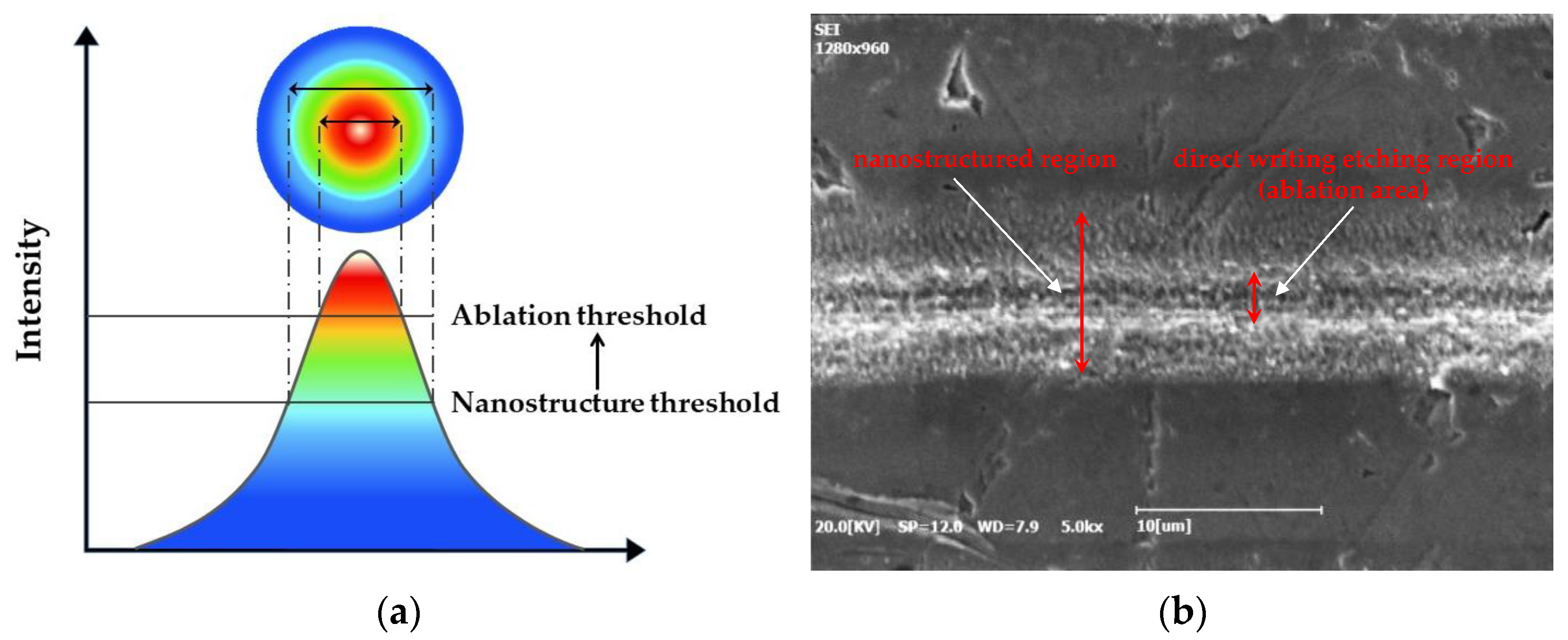
2.1. Preparation and Characterization of Micro–Nano Structure

The femtosecond laser experimental apparatus for processing micro–nano grating structures on a tungsten target includes three main components: an external optical path system, a direct writing processing system, and a sample translation stage. The femtosecond laser source utilizes the Coherent Company’s Ti-sapphire femtosecond laser (LEGEND ELITE, Coherent, Saxonburg, PA, USA). The specific parameters are as follows: a center wavelength of 800 nm, a pulse width of 35 fs, a repetition rate of 1 kHz, and a maximum single pulse energy of 3.5 mJ. The laser pulse’s fluence could be continuously adjusted using a neutral attenuator. Once the required fluence was set, the femtosecond laser was directed onto the Olympus microscope system (Olympus, Tokyo, Japan). Within the Olympus microscope system, the beam was focused on a 99.99% pure tungsten target surface using an objective lens with a magnification of 10× and a numerical aperture of 0.25. To process surface grating structures with varying periods, the scanning speed and trajectory of the Newport three-dimensional precision translation stage were adjusted (Note: the experiment was conducted in an air environment).
The control script was input into the electronic control translation stage, and the scanning speed was set to 1 mm/s. After the x-axis moved X mm, the y-axis moved P μm. Then the x-axis moved X mm in the opposite direction, and the y-axis moved P μm. This ‘S’-shaped path scanning was repeated, and finally, a one-dimensional grating structure with a period of P μm was obtained. Simultaneously, by adjusting the neutral attenuator, the femtosecond laser fluences were set to 0.64 J/cm2, 1.27 J/cm2, 1.91 J/cm2, …, 9.55 J/cm2. Different laser fluences were used to process the tungsten. After direct writing, the samples were placed in ethanol and cleaned using an ultrasonic cleaner. Once dried, their surface morphology was characterized using scanning electron microscopy (SEM, Coxem, Daejeon, Republic of Korea) and atomic force microscopy (AFM, Being Nano-Instruments, Beijing, China). The study established the relationship between different experimental parameters, such as femtosecond laser fluence, scanning speed, and grating structure. Additionally, the surface micro–nano structures were measured using a Bruker Fourier infrared spectrometer (Vertex 70, Bruker, Berlin, Germany) for thermal radiation. We modified the measurement method of the Fourier transform infrared (FTIR) spectrometer (Vertex 70, Bruker, Germany) based on previous research. Using the FTIR interface, we introduced the heated sample into the spectrometer as an external light source. An external optical path was set up near the external light source port to collect the thermal radiation generated by the heated sample. The radiation was gathered by the off-axis parabolic mirror and directed to the external light source port of the FTIR. By doing this, we were able to obtain the thermal radiation spectrum of the samples.
As a result, we analyze how grating structures processed with different laser fluences affect thermal radiation characteristics. Furthermore, we explore the impact of temperature on the thermal radiation characteristics of tungsten targets with specific grating structures. The thermal radiation infrared spectrum measurement device is illustrated in Figure 1.

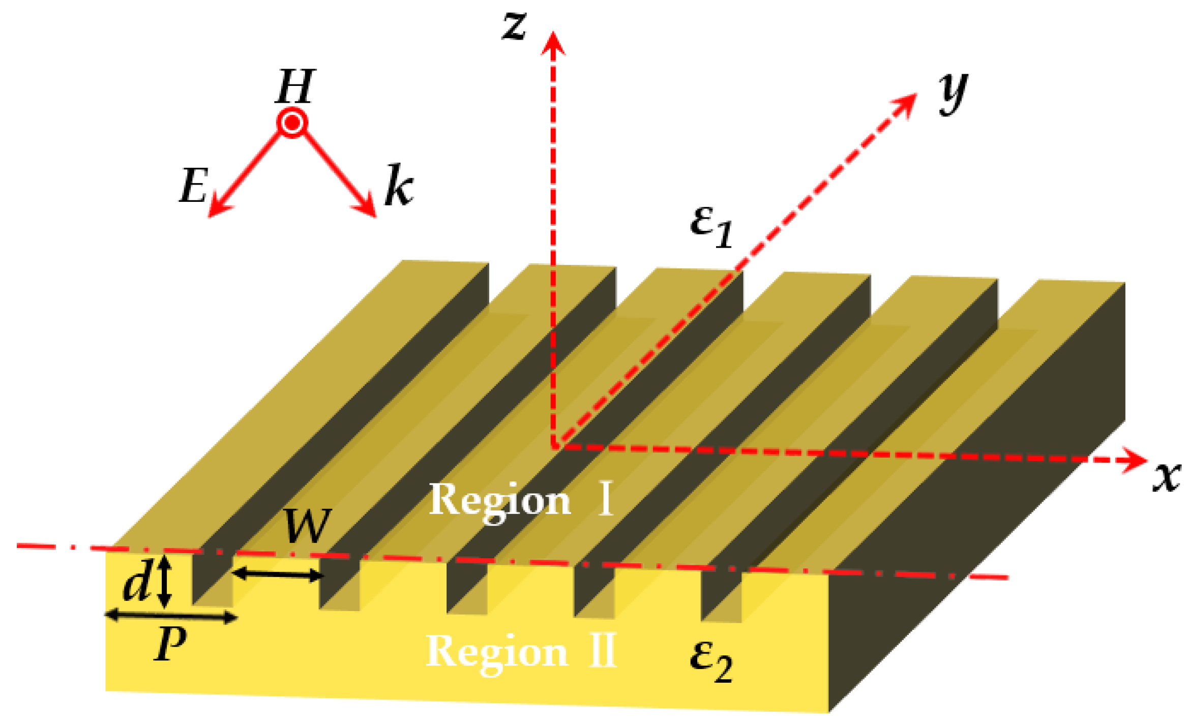
2.2. Simulation Method and Model Design

The simulation utilizes COMSOL Multiphysics software (COMSOL Multiphysics 5.6), which is based on finite element analysis and multi-physics coupling. It can accurately simulate and predict the process of light–matter interaction in optical simulations. In COMSOL, the most commonly used method for electromagnetic field calculation assumes that the electromagnetic field is a first-order time-harmonic field, with the time-independent part being a vector field with complex values. The solution is performed at a certain time-harmonic frequency, known as frequency domain electromagnetic simulation. When working with time-harmonic fields in COMSOL, the frequency domain simulation is used to solve the Helmholtz equation for the electric and magnetic fields. The main modeling steps in COMSOL Multiphysics are as follows: 1. Select the relevant physical fields and research content. 2. Model the geometric structure. 3. Set the material properties. 4. Define the boundary conditions. 5. Create the mesh. 6. Run the operation and perform the calculations.
In this study, we modeled the surface grating structure and simulated the emission spectra of gratings with different periodic structure parameters. We then compared these simulated results with experimental data. Figure 2 displays the schematic diagram illustrating the interaction between electromagnetic waves and micro–nano periodic structures. The structural parameters include the grating period (P), width (W), and depth (d). Meanwhile, the specific parameters were adjusted based on the experimentally prepared grating structure. Because the grating structure was periodic, the simulation was carried out in a two-dimensional plane. The periodic condition was set as the Floquet period, and the appropriate grid accuracy was divided according to the physical field.

3. Results and Discussion

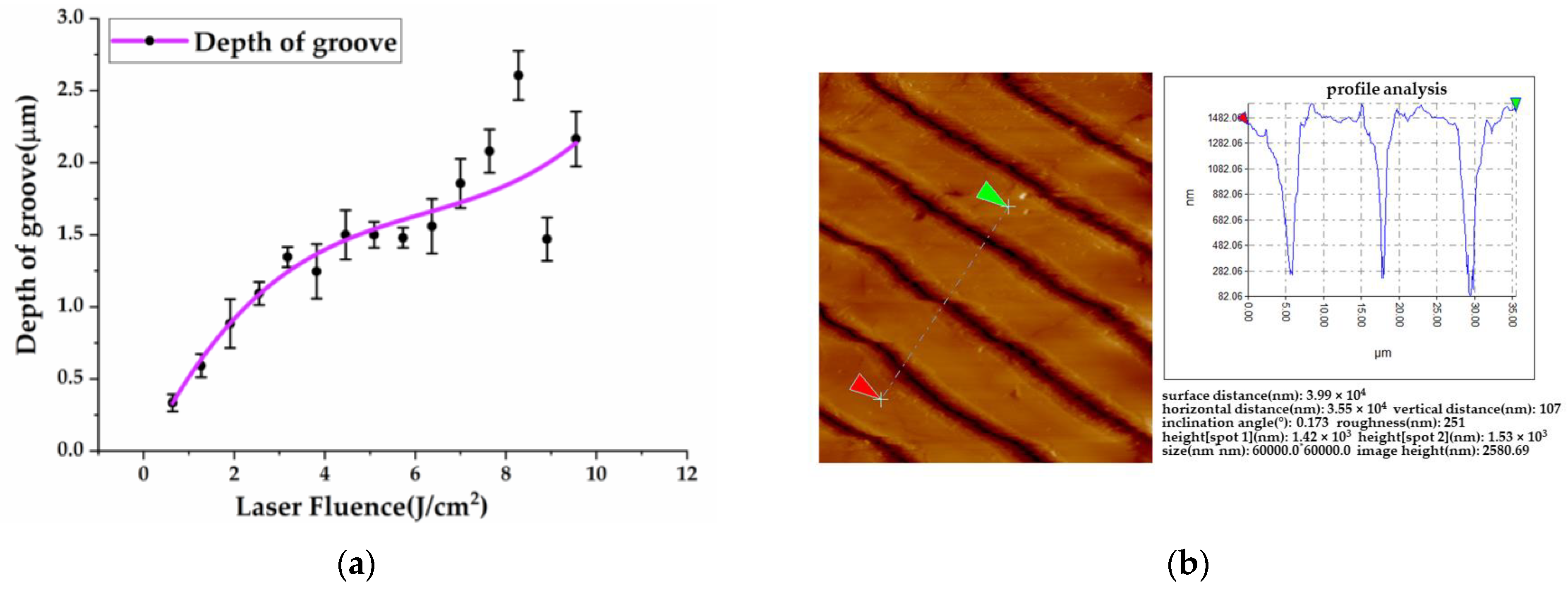
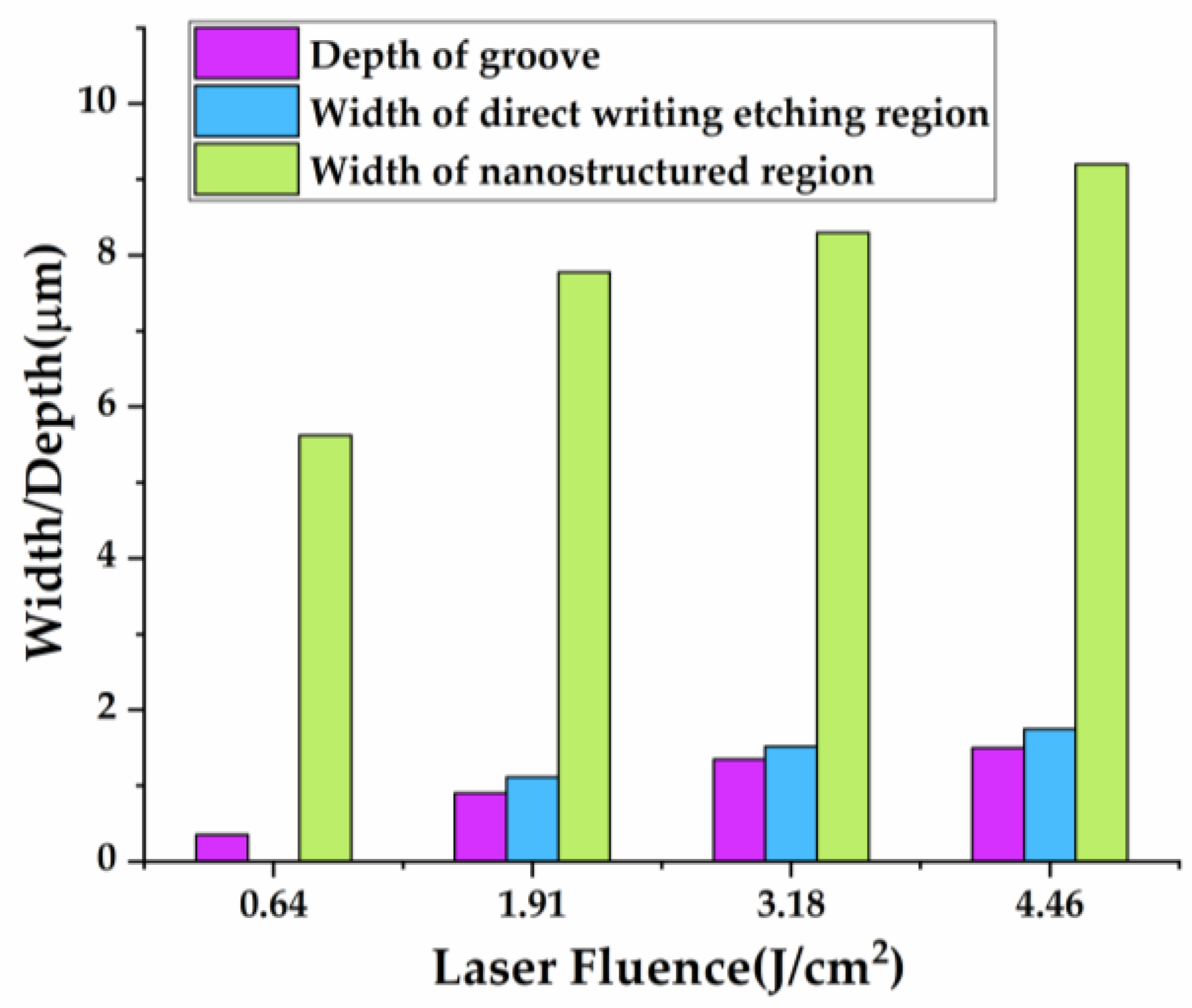
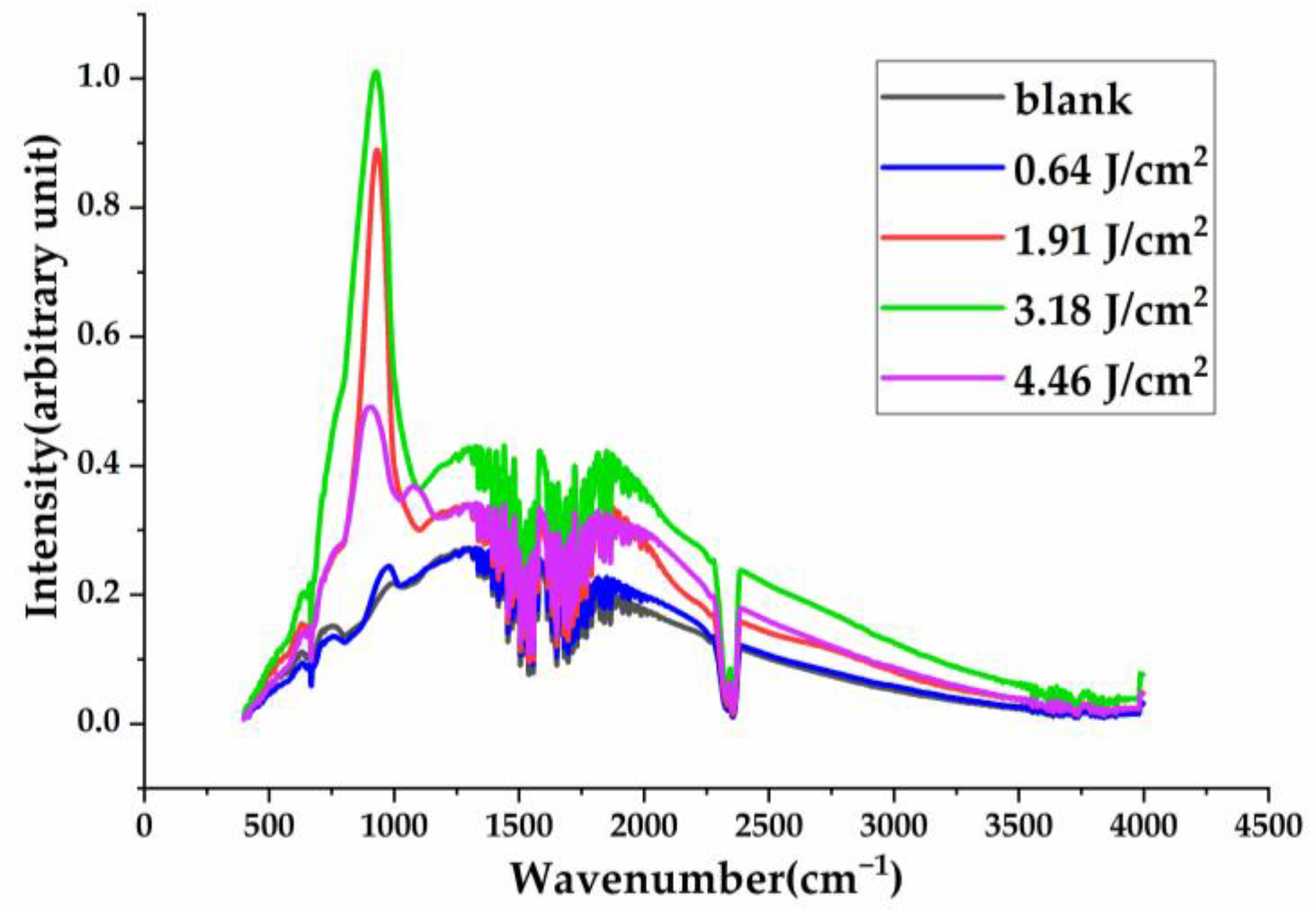
3.1. The Influence of Varying Laser Fluence on the Grating Structure

In our experiments, we find that when the laser energy density is 0.64 J/cm2, an ablation area starts to appear on the surface of the tungsten. The laser ablation threshold depends not only on the material’s properties but also on the laser parameters. The pulse width is a crucial parameter that affects the ablation threshold. For long pulse lasers with a pulse width above nanoseconds, the ablation threshold is reflected in statistical characteristics. In the case of ultrashort pulse lasers, the statistical properties of the ablation threshold may not be readily apparent because of the predominant influence of nonlinear effects. The Gaussian distribution of the femtosecond laser beam results in high intermediate energy and low edge energy. The high intermediate energy surpasses the material’s ablation threshold, leading to the formation of a direct writing etching region. On the other hand, the relatively weak edge energy fails to reach the ablation threshold, resulting in the formation of a nanostructured region. Figure 3 illustrates the clear definition of the nanostructured region and the direct writing etching region.
In this study, we explore the impact of different laser fluences on the depth of the grating structure’s grooves, as illustrated in Figure 4a. We maintained a scanning speed of 1 mm/s while increasing the laser fluence from 0.64 J/cm2 to 9.55 J/cm2. To analyze the data, we used polynomial fitting. Polynomial fitting offers high flexibility, better reflects data trends, and involves simple calculations. After optimizing the fitting process, we achieved an R-squared correlation coefficient of over 0.9. This indicates that the fitted curve closely matches the data, demonstrating the feasibility of the fitting process. In Figure 4a, it is evident that the depth of the groove increases as the femtosecond laser fluence increases. At a laser fluence of 0.64 J/cm2, the depth of the groove is 0.35 μm. However, when the laser fluence is increased to 8.28 J/cm2, the groove depth also increases to 2.6 μm, and the maximum error is 0.195 μm. As the laser fluence and energy increase, the ablation of the target also increases, resulting in a greater depth of the groove.
It is crucial to consider several factors when studying the grating structure, such as the period, the depth of the groove, the size of the nanostructure region, and the direct writing etching region. This study specifically focuses on how the femtosecond laser fluence influences the ablation area of the grating structure. The translation stage’s scanning speed was 1 mm/s, and the grating period was 20 μm. By adjusting the femtosecond laser fluence using a neutral attenuator, ranging from 0.64 J/cm2 to 9.55 J/cm2, we were able to process a tungsten target under varying laser fluence. The grating period measured by SEM was consistent with the procedure’s setting. Figure 5 demonstrates how the width of the nanostructured region and the direct writing etching region is influenced by varying laser fluence. In addition, a polynomial fitting was used, and the correlation coefficient R-squared was over 0.9. Observing Figure 5a,b, it is evident that both the width of the nanostructured region and the width of the direct writing etching region increase as the femtosecond laser fluence increases. At a laser fluence of 0.64 J/cm2, the width of the nanostructured region is the smallest at 5.62 μm, while at 9.55 J/cm2, the width of the nanostructured region is the largest at 10.575 μm, and the maximum error of the width of 0.203 μm.
The femtosecond laser beam has a Gaussian distribution, resulting in high intermediate and low edge energy. The high intermediate energy reaches the material’s ablation threshold, creating a direct writing etching region. The low edge energy does not reach the ablation threshold, resulting in a nanostructured region. Additionally, different laser fluences cause varying light intensity distributions, leading to different widths of the grating nanostructure and the direct writing etching regions.
The surface morphology of the prepared grating structure could be characterized using a scanning electron microscope (SEM, Coxem, Republic of Korea). The grating structure period, the size of the nanostructure region, and the direct writing etching region could be measured. Figure 6 displays the SEM images of the grating structure prepared at the laser fluence of 1.91 J/cm2, 3.18 J/cm2, and 4.46 J/cm2. Meanwhile, the scanning speed during the process was 1 mm/s, and the period was 20 μm. Figure 6 demonstrates that the micro–nano periodic structure, processed by femtosecond laser direct writing technology, is consistent with the period set by the program, and its surface arrangement is regular and orderly. The laser etching processes micron-level deep grooves with many sub-wavelength nanostructures along the edges. Almost no heat-affected area exists, and microcracks around the groove are not obvious. Significantly, the processing system is simple and does not require harsh conditions. Experiments can be carried out at room temperature in air. This technology can process various structure parameters and large-area micro–nano periodic structures to meet the needs of different fields for periodic grating structures.
When the pulse energy approaches the material’s ablation threshold, a grating structure with a period smaller than the laser wavelength can be directly induced, known as a laser-induced periodical surface structure (LIPSS) [56,57,58,59,60,61,62]. Generally, LIPSSs are believed to be generated by the interference between the incident light and the surface plasmon polaritons. LIPSSs usually emerge when the laser fluence is low. Furthermore, LIPSSs gradually decrease as the laser fluence increases [63,64,65,66]. Figure 6 illustrates the magnified SEM image of LIPSSs.

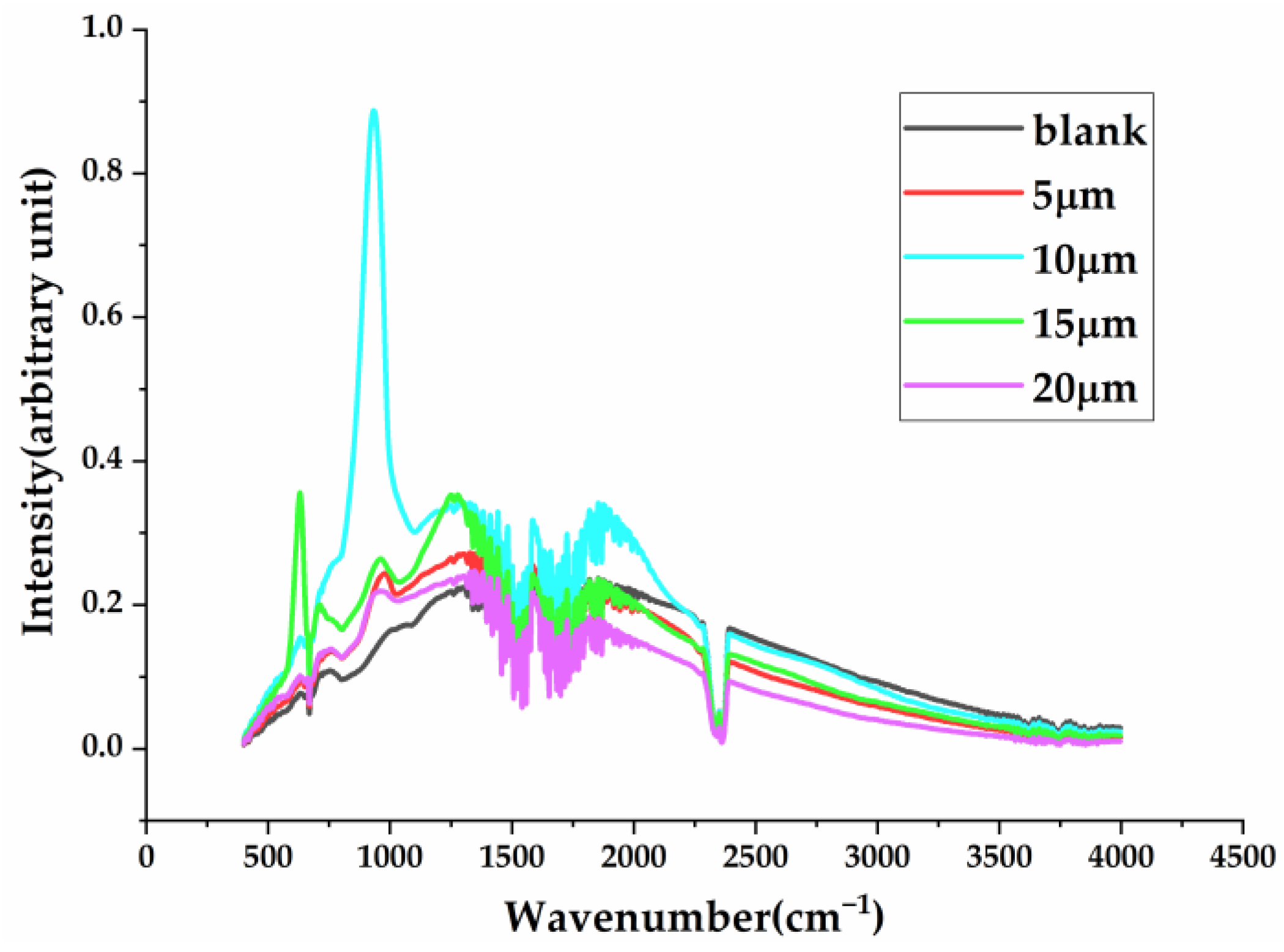
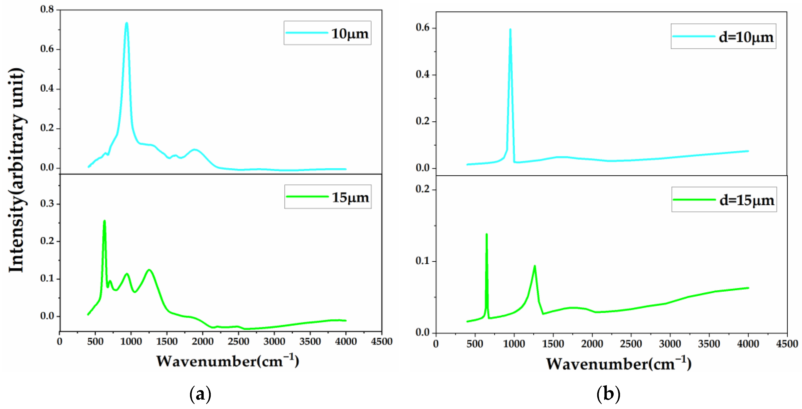
3.2. The Influence of Different Grating Structures on the Thermal Radiation Spectrum

The above experiments explored the impact of varying laser fluence on several parameters, including the depth of the groove, the width of the nanostructure region, and the width of the direct writing etching region. In this section, we measured a blank tungsten target sample and a tungsten target with grating structures that were processed using laser fluences of 0.64 J/cm2, 1.91 J/cm2, 3.18 J/cm2, and 4.46 J/cm2. We conducted the measurements using FTIR. The processing scanning speed was 1 mm/s, the period of the grating structure was 10 μm, and the parameters of the grating structures for each laser fluence are depicted in Figure 7.
The spectrometer detector utilized in the experiment was DTGS, and the beam splitter was KBr. The measured infrared spectrum ranged from 400 cm−1 to 4000 cm−1, and the heating temperature was 300 °C. At 300 °C, the thermal radiation energy is primarily concentrated in the infrared region. Additionally, the scanning speed was 1 mm/s, and the grating period was 10 μm. Figure 8 illustrates the thermal radiation spectrum display absorption bands caused by water and carbon dioxide at wavenumbers of 2350 cm−1 and 1625 cm−1. As the laser fluence increases, a thermal emission enhancement peak starts to emerge near the wavenumber of 900 cm−1 when the laser fluence reaches 1.91 J/cm2. The enhanced peak of thermal radiation is generated due to the emission of thermally excited particles from the heated material’s surface, which is coupled with the surface grating structure. The resonance excites the surface plasmon polaritons, enhancing the intensity of the resonance excitation on the surface (Appendix A provides the relevant theoretical foundations). Consequently, the electromagnetic wave in the infrared band emitted by the far field has an amplified peak that aligns with the resonance frequency of the surface plasmon polaritons. Even though there are LIPSSs at the edge of the structure when the laser fluence is low, the wavelength of the thermal radiation enhancement peak is consistent with the period of the grating structure. As the laser fluence increases, the LIPSSs gradually decrease. Therefore, we believe that the change in thermal radiation is primarily due to the periodic grating structure.
As the laser fluence increases, the radiation enhancement peak’s intensity initially increases and then decreases. This happens because the laser fluence determines the extent of ablation and volatilization during the laser-material interaction process. Higher laser fluence makes the resulting surface structure more noticeable, and the thermal radiation enhancement characteristics become more pronounced. However, when the laser fluence is too large, dense and complex micro–nano structures will form on the material’s surface, which absorbs the emitted thermal radiation. As a result, the intensity of the thermal radiation decreases as the fluence increases beyond a certain point.
Furthermore, we notice that the position of the enhancement peak shifts when the laser influence reaches 4.46 J/cm2. Meanwhile, a new weaker enhancement peak appears. Following a discussion and a review of the literature, we believe this is attributable to variations in the depth of the grating structure. As shown in Section 3.1, different laser fluences can prepare grating structures with varying depths. We think the enhancement peak of the thermal radiation spectrum exhibits a red shift as the depth increases within a certain range. Consequently, we could observe the peak shifting towards lower wavenumbers, while a second-order enhancement peak appears. Our discussion is consistent with the point presented in the previous literature [21]. While our current work does not systematically explore this result, we consider it an interesting finding and a potential research direction for further work.
Grating structures with periods of 5 μm, 10 μm, 15 μm, and 20 μm were processed using a femtosecond laser with a laser fluence of 3.18 J/cm2. The processing scanning speed was maintained at 1 mm/s. The thermal radiation spectrum of the grating structure for each period was tested, and the results are presented in Figure 9. For the grating period of 5 μm, a thermal radiation enhancement peak is observed near the wavenumber of 900 cm−1. Subsequently, for the grating period of 10 μm, the intensity of the thermal radiation peak near 900 cm−1 shows a significant increase. At a grating period of 15 μm, there is a thermal radiation enhancement peak near the wavenumber of 650 cm−1. However, when the grating period is 20 μm, the thermal radiation enhancement peak basically disappears, and the thermal radiation spectrum is nearly identical to the spectrum of the blank tungsten target. Therefore, when the grating structure period is too large, it has no obvious effect on the thermal radiation characteristics.
In addition, we compared the maximum radiation intensity of a blank sample to samples with different periods. The maximum radiation intensity of the sample with a period of 5 μm is approximately 1.2 times that of the blank sample; for the sample with a period of 10 μm, it is about 3.7 times; for the sample with a period of 15 μm, it is about 1.5 times; and for the sample with a period of 20 μm, it is almost equal to the blank sample.
We subtracted the thermal emission spectra of the blank tungsten sample from the spectra of different periods to perform spectral subtraction. Then, we eliminated the absorption bands caused by carbon dioxide and water vapor in the air. Finally, the thermal radiation spectrum of relative intensity was obtained. In Figure 10, we can see the maximum relative intensity for different periods: at 5 μm, it is approximately 0.09; at 10 μm, it is about 0.74; at 15 μm, it is around 0.26; and at 20 μm, it is roughly 0.08. The enhancement effect on thermal radiation is more significant when the period is 10 μm or 15 μm. In Figure 10, the position of the thermal radiation enhancement peak of the grating structure with different periods is intuitive, and the second-order enhancement peak can be observed in the grating structure of 10 and 15 μm, which is due to the Floquet–Bloch wave vector of the grating structure k g = 2 π m / Λ in the order m = 2.
Based on the optical parameters of tungsten found in the literature, we used COMSOL Multiphysics software to calculate the reflectivity of grating structures with periods of 10 μm and 15 μm. We then converted these values to emissivity using Kirchhoff’s thermal radiation law. Our simulation results are depicted in Figure 11. It is evident from the results that the calculated enhancement peak of the 10 μm grating structure occurs near the wavenumber of 900 cm−1, while the enhancement peak of the 15 μm grating structure is near the wavenumber of 650 cm−1. The experimental results are consistent with the simulation results, indicating that the position of the peak for enhanced thermal emission can be effectively altered by adjusting the period of the grating structure. This allows for selective spectrum regulation.

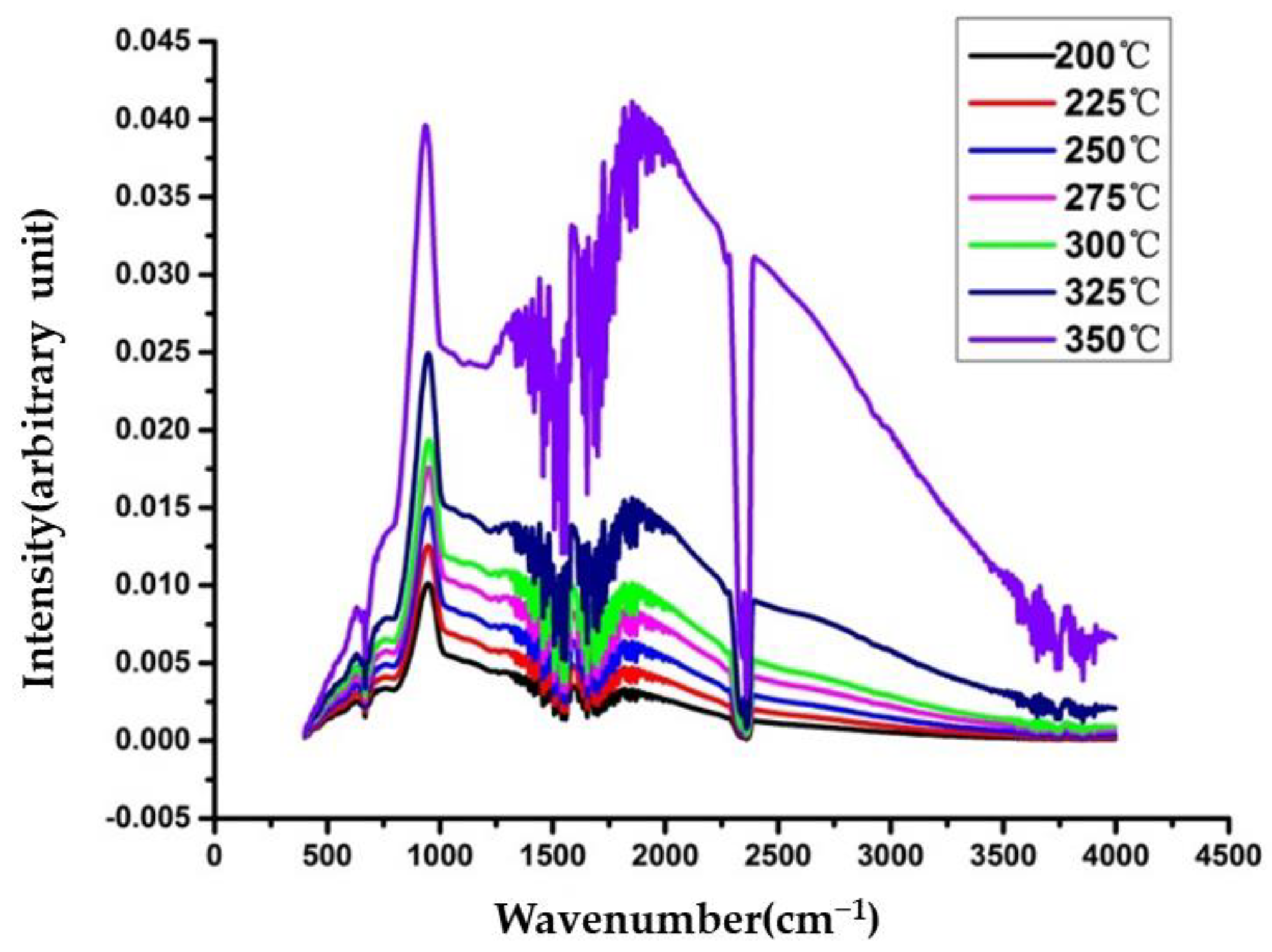
3.3. The Effect of Varying Heating Temperatures on the Thermal Radiation Spectrum

In this part, the grating structure was processed with a period of 10 μm and a laser fluence of 3.18 J/cm2. At the same time, the scanning speed was 1 mm/s. The spectra obtained at different temperatures were used to analyze how the thermal radiation spectrum characteristics of the tungsten target surface with a grating structure were affected by temperature variations. Figure 12 displays the thermal radiation spectra measured at heating temperatures ranging from 200 °C to 350 °C with intervals of 25 °C. Figure 12 shows a significant peak in the thermal radiation spectrum at around 900 cm−1, along with absorption bands from water and carbon dioxide at 2350 cm−1 and 1625 cm−1, respectively. First, we notice that the positions of the enhancement peaks remain constant as the temperature changes. Additionally, the thermal radiation at all wavenumbers increases with rising temperature. Finally, the relative weighting given to different wavenumbers changes with varying temperatures because the peak of the Planck distribution shifts toward lower wavelengths as temperature increases. In our work, the peaks near 1850 cm−1 are insignificant features at 200 °C but became more prominent at 350 °C because the blackbody’s spectra shift in such a way that it gives those peaks much more weight than before.

4. Conclusions

In this paper, processed grating structures on a tungsten target used femtosecond laser writing to explore their effect on thermal radiation spectral characteristics. Firstly, the effects of varying laser fluence on the grating structure are researched. As the laser fluence increases, the depth of the groove, the width of the nanostructured region, and the width of the direct writing etching region all show an increasing trend. Secondly, the influence of different laser fluences on thermal radiation is studied. When the laser fluence is 1.91 J/cm2 and the period is 10 um, the peak of thermal radiation enhancement appears near the wavenumber of 900 cm−1. Its intensity increases initially and then decreases with the increase of laser fluence. Additionally, the influence of different periods on thermal radiation is explored. It is observed that the positions of enhanced peaks vary with different periods. When the grating period is too large, the effect is not evident. Finally, the impact of various heating temperatures on thermal radiation is also researched. Heating temperature is a significant factor affecting the intensity of thermal radiation. First, the positions of the enhancement peaks remain constant despite temperature changes. Second, the thermal radiation at all wavenumbers increases with the increasing temperature. Third, the relative weighting given to different wavenumbers changes with temperature increase.
The results demonstrate that controlling thermal radiation can be realized by processing periodic structures on the material. In recent years, with the continuous progress of science and technology, various fields have increasingly demanded specific thermal radiation characteristics. The desired thermal radiation characteristics can be attained by fabricating a grating structure on the material’s surface. This approach can find wide applications in the aerospace field, including in infrared remote sensing, infrared detection, and infrared guidance. Moreover, it can be utilized in infrared switches, medical care, remote controls, infrared interfaces, and anti-theft devices, benefiting different aspects of human production and daily life.

Author Contributions

Conceptualization, H.S.; methodology, R.G.; validation, P.Z.; formal analysis, W.Z., H.S.; investigation, R.G.; resources, R.G. and W.Z.; data curation, R.G. and W.Z.; writing—original draft preparation, R.G. and P.Z.; writing—review and editing, R.G. and P.Z.; supervision, H.S.; funding acquisition, S.L. All authors have read and agreed to the published version of the manuscript.

Funding

Prof. Liu gratefully acknowledges support from the National Natural Science Foundation of China (Grant No. 51875006).

Institutional Review Board Statement

Not applicable.

Informed Consent Statement

Not applicable.

Data Availability Statement

Data can be made available upon request from the authors.

Acknowledgments

Ruxue Guo thanks Yanjie Zhang and Song Liu for the help in the theoretical analysis and experiments discussions.

Conflicts of Interest

The authors declare no conflicts of interest.

Appendix A

When a beam of visible or infrared light is incident on an interface, the free electron density on the metal surface causes a collective oscillation due to the coupling effect of the incident electromagnetic wave. Surface plasmon polaritons (SPPs), generated by this interaction, are excited by electromagnetic waves and display electromagnetic characteristics. Consequently, SPPs obey the basic electromagnetic field equations, i.e., Maxwell’s equations. The dispersion properties of surface plasmon polaritons are derived from Maxwell’s equations.
The differential form of Maxwell’s equations is
{ × H = σ E + ε 0 ε E t × E = μ 0 H t · H = 0 · E = ρ
Here, E represents the electric field, H represents the magnetic field, ε is the dielectric constant of the medium, σ is the conductivity of the medium, μ 0 is the permeability of the medium, and ρ is the bulk charge density of the medium. The first two terms of the Equation (A1) are taken curl respectively, and if the infinite homogeneous medium σ = 0 , the equation is simplified as follows:
{ 2 E μ 0 ε ε 0 2 E t 2 = 0 2 H μ 0 ε ε 0 2 H t 2 = 0
When the field changes harmonically with time, the Helmholtz equation can be obtained from Equation (A2):
{ 2 E + k 0 2 ε r E = 0 2 B + k 0 2 ε r B = 0
where k 0 = ε 0 μ 0 ω , ε r = ( ε + i σ ω ε 0 ) is the complex dielectric function of the material. Suppose that the electric field propagating along the x direction is E = E ( z ) e i β x , and β is the wave vector propagating along the x direction. Substituting it into Equation (A3), we can obtain the following:
2 E ( z ) z 2 + ( k 0 2 ε β 2 ) E = 0
Suppose the electric field E = ( E x + E y + E z ) e i ω t , the magnetic field H = ( H x + H y + H z ) e i ω t , and substitute into Equation (A4), after simplification, two sets of solutions of TM mode and TE mode can be obtained, which are represented by the following equations, respectively:
{ E x = i 1 ω ε ε 0 H y z E z = i β ω ε ε 0 H y 2 H y z 2 + ( k 0 2 ε β 2 ) H y = 0
{ H x = i 1 ω μ E y z H z = β ω μ E y 2 E y z 2 + ( k 0 2 ε β 2 ) E y = 0
When z > 0 , the electric field wave vector is k 1 and the dielectric constant is ε 1 ; when z < 0 , the electric field wave vector is k 2 , the dielectric constant is ε 2 , and the boundary condition is
k 2 k 1 = ε 2 ε 1
It can be seen from the above formula that the existence of surface waves requires the real part of the dielectric function at both ends of the interface to be different. Equations can be obtained from (A7):
{ k 1 2 = β 2 k 0 2 ε 1 k 2 2 = β 2 k 0 2 ε 2
Substituting the boundary conditions into the equation set (A8), the dispersion relation of SPPs can be obtained as follows:
k s p p = β = k 0 ε 1 ε 2 ε 1 + ε 2
Similarly, for the TE mode, we can obtain
E y ( k z 1 + k z 2 ) = 0
Since both k z 1 and k z 2 are positive, the equation is satisfied only when E y 1 = E y 2 = 0 . Consequently, there are no surface plasmon polaritons associated with TE polarization; that is, SPPs can only exist in the context of TM polarization.

References

  1. Modest, M.F.; Mazumder, S. Radiative Heat Transfer; Academic Press: Cambridge, MA, USA, 2021. [Google Scholar]
  2. Gray, W.A.; Müller, R. Engineering Calculations in Radiative Heat Transfer: International Series on Materials Science and Technology; Elsevier: Amsterdam, The Netherlands, 2013; Volume 13. [Google Scholar]
  3. Li, W.; Fan, S.H. Nanophotonic control of thermal radiation for energy applications [Invited]. Opt. Express 2018, 26, 15995–16021. [Google Scholar] [CrossRef] [PubMed]
  4. Coutts, T.J. An overview of thermophotovoltaic generation of electricity. Sol. Energy Mater. Sol. Cells 2001, 66, 443–452. [Google Scholar] [CrossRef]
  5. Inoue, T.; De Zoysa, M.; Asano, T.; Noda, S. Realization of dynamic thermal emission control. Nat. Mater. 2014, 13, 928–931. [Google Scholar] [CrossRef] [PubMed]
  6. Zhang, X.S.; Chen, Y.J.; Hu, J.L. Recent advances in the development of aerospace materials. Prog. Aerosp. Sci. 2018, 97, 22–34. [Google Scholar] [CrossRef]
  7. Tian, J.L.; Zhang, W.; Gu, J.J.; Deng, T.; Zhang, D. Bioinspired Au-CuS coupled photothermal materials: Enhanced infrared absorption and photothermal conversion from butterfly wings. Nano Energy 2015, 17, 52–62. [Google Scholar] [CrossRef]
  8. Lenert, A.; Bierman, D.M.; Nam, Y.; Chan, W.R.; Celanovic, I.; Soljacic, M.; Wang, E.N. A nanophotonic solar thermophotovoltaic device. Nat. Nanotechnol. 2014, 9, 126–130. [Google Scholar] [CrossRef]
  9. Zhao, B.; Santhanam, P.; Chen, K.F.; Buddhiraju, S.; Fan, S.H. Near-Field Thermophotonic Systems for Low-Grade Waste-Heat Recovery. Nano Lett. 2018, 18, 5224–5230. [Google Scholar] [CrossRef] [PubMed]
  10. Wang, Z.L.; Zhang, Z.M.; Quan, X.J.; Cheng, P. A perfect absorber design using a natural hyperbolic material for harvesting solar energy. Sol. Energy 2018, 159, 329–336. [Google Scholar] [CrossRef]
  11. Molesky, S.; Jacob, Z. Ideal near-field thermophotovoltaic cells. Phys. Rev. B 2015, 91, 205435. [Google Scholar] [CrossRef]
  12. Navarro-Baena, I.; Jacobo-Martín, A.; Hernández, J.J.; Smirnov, J.R.C.; Viela, F.; Monclús, M.A.; Osorio, M.R.; Molina-Aldareguia, J.M.; Rodríguez, I. Single-imprint moth-eye anti-reflective and self-cleaning film with enhanced resistance. Nanoscale 2018, 10, 15496–15504. [Google Scholar] [CrossRef] [PubMed]
  13. Huang, Z.J.; Shi, X.Y.; Wang, G.; Leukkunen, P.; Huttula, M.; Cao, W. Antireflective design of Si-based photovoltaics via biomimicking structures on black butterfly scales. Solar Energy 2020, 204, 738–747. [Google Scholar] [CrossRef]
  14. Liu, Y.; Song, Y.Y.; Niu, S.C.; Zhang, Y.L.; Han, Z.W.; Ren, L.Q. Integrated super-hydrophobic and antireflective PDMS bio-templated from nano-conical structures of cicada wings. RSC Adv. 2016, 6, 108974–108980. [Google Scholar] [CrossRef]
  15. Fan, S.H. Thermal Photonics and Energy Applications. Joule 2017, 1, 264–273. [Google Scholar] [CrossRef]
  16. Liu, S.; Song, H.Y.; Wang, S.N.; Du, B.R.; Wang, B.; Emara, E.M.; Liu, S.B. Surface micro-nano hydrophobic structuring on silver-coated semiconductor substrate by femtosecond laser irradiation. J. Laser Appl. 2022, 34, 012019. [Google Scholar] [CrossRef]
  17. Zhang, Z.Y.; Gu, Q.M.; Jiang, W.; Zhu, H.; Xu, K.; Ren, Y.P.; Xu, C. Achieving of bionic super-hydrophobicity by electrodepositing nano-Ni-pyramids on the picosecond laser-ablated micro-Cu-cone surface. Surf. Coat. Technol. 2019, 363, 170–178. [Google Scholar] [CrossRef]
  18. Yang, G.F.; Zhang, H.; Li, H.W.; Lu, M.K.; Zhai, W.; Cui, J. Experimental study on the ice suppression characteristics of TC4 microstructure surface induced by femtosecond pulsed laser. Surf. Coat. Technol. 2021, 405, 126558. [Google Scholar] [CrossRef]
  19. Langevin, D.; Verlhac, C.; Jaeck, J.; Abou-Hamdan, L.; Taupeau, E.; Fix, B.; Bardou, N.; Dupuis, C.; De Wilde, Y.; Haidar, R.; et al. Experimental Investigation of the Thermal Emission Cross Section of Nanoresonators Using Hierarchical Poisson-Disk Distributions. Phys. Rev. Lett. 2024, 132, 043801. [Google Scholar] [CrossRef] [PubMed]
  20. De Zoysa, M.; Asano, T.; Mochizuki, K.; Oskooi, A.; Inoue, T.; Noda, S. Conversion of broadband to narrowband thermal emission through energy recycling. Nat. Photonics 2012, 6, 535–539. [Google Scholar] [CrossRef]
  21. Ma, X.R.; Du, B.R.; Tan, S.W.; Song, H.Y.; Liu, S.B. Spectral Characteristics Simulation of Topological Micro-Nano Structures Based on Finite Difference Time Domain Method. Nanomaterials 2021, 11, 2622. [Google Scholar] [CrossRef] [PubMed]
  22. Guo, X.J.; Song, H.Y.; Du, B.R.; Tan, S.W.; Liu, S.B. Study on Spectral Selective Manipulation Characteristics of Surface Multilevel Micro-Nano Structures by FDTD Simulation. Int. J. Mol. Sci. 2022, 23, 2774. [Google Scholar] [CrossRef] [PubMed]
  23. Arpin, K.A.; Losego, M.D.; Cloud, A.N.; Ning, H.L.; Mallek, J.; Sergeant, N.P.; Zhu, L.X.; Yu, Z.F.; Kalanyan, B.; Parsons, G.N.; et al. Three-dimensional self-assembled photonic crystals with high temperature stability for thermal emission modification. Nat. Commun. 2013, 4, 2630. [Google Scholar] [CrossRef]
  24. Chan, D.L.C.; Soljacic, M.; Joannopoulos, J.D. Thermal emission and design in 2D-periodic metallic photonic crystal slabs. Opt. Express 2006, 14, 8785–8796. [Google Scholar] [CrossRef] [PubMed]
  25. Yokoyama, T.; Dao, T.D.; Chen, K.; Ishii, S.; Sugavaneshwar, R.P.; Kitajima, M.; Nagao, T. Spectrally Selective Mid-Infrared Thermal Emission from Molybdenum Plasmonic Metamaterial Operated up to 1000 °C. Adv. Opt. Mater. 2016, 4, 1987–1992. [Google Scholar] [CrossRef]
  26. Coppens, Z.J.; Valentine, J.G. Spatial and Temporal Modulation of Thermal Emission. Adv. Mater. 2017, 29, 1701275. [Google Scholar] [CrossRef] [PubMed]
  27. Jin, W.L.; Polimeridis, A.G.; Rodriguez, A.W. Temperature control of thermal radiation from composite bodies. Phys. Rev. B 2016, 93, 121403. [Google Scholar] [CrossRef]
  28. Liu, B.A.; Gong, W.; Yu, B.W.; Li, P.F.; Shen, S. Perfect Thermal Emission by Nanoscale Transmission Line Resonators. Nano Lett. 2017, 17, 666–672. [Google Scholar] [CrossRef]
  29. Li, J. Thermal Radiation from Nanophotonic Structures: Theory, Numerical Simulation and Applications. Ph.D. Thesis, Carnegie Mellon University, Pittsburgh, PA, USA, 2020. Available online: https://www.proquest.com/dissertations-theses/thermal-radiation-nanophotonic-structures-theory/docview/2457933729/se-2 (accessed on 15 August 2024).
  30. Yu, H.Y.; Zhang, H.C.; Wang, H.M.; Zhang, D. The Equivalent Thermal Conductivity of the Micro/Nano Scaled Periodic Cubic Frame Silver and Its Thermal Radiation Mechanism Analysis. Energies 2021, 14, 4158. [Google Scholar] [CrossRef]
  31. Bikbaev, R.G.; Vetrov, S.Y.; Timofeev, I.V. Hybrid Tamm and surface plasmon polaritons in resonant photonic structure. J. Quant. Spectrosc. Radiat. Transf. 2020, 253, 107156. [Google Scholar] [CrossRef]
  32. Ge, C.X.; Wu, Z.S.; Bai, J.; Gong, L. Effect of nanoscale roughness on optical trapping properties of surface plasmon polaritons exerted on nanoparticle. J. Quant. Spectrosc. Radiat. Transf. 2018, 219, 339–349. [Google Scholar] [CrossRef]
  33. Wang, Q.; Yuan, G.H.; Kiang, K.S.; Sun, K.; Gholipour, B.; Rogers, E.T.F.; Huang, K.; Ang, S.S.; Zheludev, N.I.; Teng, J.H. Reconfigurable phase-change photomask for grayscale photolithography. Appl. Phys. Lett. 2017, 110, 201110. [Google Scholar] [CrossRef]
  34. Sai, H.; Yugami, H. Thermophotovoltaic generation with selective radiators based on tungsten surface gratings. Appl. Phys. Lett. 2004, 85, 3399–3401. [Google Scholar] [CrossRef]
  35. Sai, H.; Yugami, H.; Kanamori, Y.; Hane, K. Spectrally selective thermal radiators and absorbers with periodic microstructured surface for high-temperature applications. Microscale Thermophys. Eng. 2003, 7, 101–115. [Google Scholar] [CrossRef]
  36. Mason, J.A.; Adams, D.C.; Johnson, Z.; Smith, S.; Davis, A.W.; Wasserman, D. Selective thermal emission from patterned steel. Opt. Express 2010, 18, 25192–25198. [Google Scholar] [CrossRef] [PubMed]
  37. Mason, J.A. Selective Thermal Emission and Absorption from Mid-IR Resonators and Metamaterials. Ph.D. Thesis, University of Massachusetts Lowell, Lowell, MA, USA, 2012. Available online: https://www.proquest.com/dissertations-theses/selective-thermal-emission-absorption-mid-ir/docview/1020571465/se-2 (accessed on 15 August 2024).
  38. Jiao, S.H.; Zhao, K.; Jiang, J.H.; Zhao, K.L.; Guo, Q.; Wang, J.B.; Zhang, Y.S.; Chen, G.; Cheng, Q.; Zuo, P.; et al. Metasurface with all-optical tunability for spatially-resolved and multilevel thermal radiation. Nanophotonics 2024, 13, 1645–1655. [Google Scholar] [CrossRef]
  39. Shirk, M.D.; Molian, P.A. A review of ultrashort pulsed laser ablation of materials. J. Laser Appl. 1998, 10, 18–28. [Google Scholar] [CrossRef]
  40. Bragheri, F.; Paiè, P.; Vázquez, R.M. Editorial for the Special Issue on New Trends and Applications in Femtosecond Laser Micromachining. Micromachines 2022, 13, 150. [Google Scholar] [CrossRef] [PubMed]
  41. Butkute, A.; Jonusauskas, L. 3D Manufacturing of Glass Microstructures Using Femtosecond Laser. Micromachines 2021, 12, 499. [Google Scholar] [CrossRef]
  42. He, J.; Xu, B.J.; Xu, X.Z.; Liao, C.R.; Wang, Y.P. Review of Femtosecond-Laser-Inscribed Fiber Bragg Gratings: Fabrication Technologies and Sensing Applications. Photonic Sens. 2021, 11, 203–226. [Google Scholar] [CrossRef]
  43. Yan, M.F.; Li, R.; Li, M.; Liu, S.J.; Zhou, G.; Lin, C.G.; Dai, S.X.; Song, B.N.; Zhang, W.; Xu, T.F.; et al. Fabrication of multi-focal chalcogenide glass microlens arrays based on femtosecond laser-assisted chemical etching method. Opt. Laser Technol. 2024, 174, 110601. [Google Scholar] [CrossRef]
  44. Yao, H.; Pugliese, D.; Lancry, M.; Dai, Y. Ultrafast Laser Direct Writing Nanogratings and their Engineering in Transparent Materials. Laser Photon. Rev. 2024, 2300891. [Google Scholar] [CrossRef]
  45. Li, Q.S.; Shi, H.S.; Xi, S.M.; Xu, Z.H.; Zhang, L.; Liu, Y. Femtosecond-Laser Direct-Writing Hydrogel-Based Microlens Arrays Customized with Multi-Dimensional Optical Configurations for Information Encryption. Adv. Mater. Technol. 2024, 9, 2301923. [Google Scholar] [CrossRef]
  46. Gupta, M.S.; Ameen, E.; Veeraragavan, A.; Pesala, B. Design and fabrication of grating-based filters for micro-thermophotovoltaic systems. In Proceedings of the 7th International Conference on Advances in Energy Research, Mumbai, India, 10–12 December 2019; Springer: Singapore, 2021; pp. 1113–1119. [Google Scholar] [CrossRef]
  47. Kang, Q.; Guo, K.; Zhang, X.; Wang, W.; Guo, Z. Dynamically manipulating long-wave infrared polarized thermal radiation by a vanadium dioxide metasurface. Opt. Lett. 2024, 49, 2485–2488. [Google Scholar] [CrossRef] [PubMed]
  48. Chu, Q.Q.; Zhong, F.; Shang, X.H.; Zhang, Y.; Zhu, S.N.; Liu, H. Controlling thermal emission with metasurfaces and its applications. Nanophotonics 2024, 13, 1279–1301. [Google Scholar] [CrossRef]
  49. Lin, C.J.; Li, Y.; Chi, C.; Kwon, Y.S.; Huang, J.Y.; Wu, Z.X.; Zheng, J.Z.; Liu, G.Z.; Tso, C.Y.; Chao, C.Y.H.; et al. A Solution-Processed Inorganic Emitter with High Spectral Selectivity for Efficient Subambient Radiative Cooling in Hot Humid Climates. Adv. Mater. 2022, 34, 2109350. [Google Scholar] [CrossRef] [PubMed]
  50. Abbas, M.A.; Kim, J.; Rana, A.S.; Kim, I.; Rehman, B.; Ahmad, Z.; Massoud, Y.; Seong, J.; Badloe, T.; Park, K.; et al. Nanostructured chromium-based broadband absorbers and emitters to realize thermally stable solar thermophotovoltaic systems. Nanoscale 2022, 14, 6425–6436. [Google Scholar] [CrossRef] [PubMed]
  51. Zhang, J.G.; Wen, Z.J.; Zhou, Z.J.; Zhou, D.J.; Qiu, Q.L.; Ge, J.; Zeng, Y.X.; Sun, Y.; Zhou, L.; Dai, N.; et al. Long-wavelength infrared selective emitter for thermal infrared camouflage under a hot environment. Opt. Express 2022, 30, 24132–24144. [Google Scholar] [CrossRef] [PubMed]
  52. Seo, M.; Wang, K.; Echols, J.R.; Winfrey, A.L. Microstructure deformation and near-pore environment of resolidified tungsten in high heat flux conditions. J. Nucl. Mater. 2022, 565, 153725. [Google Scholar] [CrossRef]
  53. Morcos, P.; Elwany, A.; Karaman, I.; Arróyave, R. Review: Additive manufacturing of pure tungsten and tungsten-based alloys. J. Mater. Sci. 2022, 57, 9769–9806. [Google Scholar] [CrossRef]
  54. Liu, X.L.; Tyler, T.; Starr, T.; Starr, A.F.; Jokerst, N.M.; Padilla, W.J. Taming the Blackbody with Infrared Metamaterials as Selective Thermal Emitters. Phys. Rev. Lett. 2011, 107, 045901. [Google Scholar] [CrossRef] [PubMed]
  55. Zhong, F.; Ding, K.; Zhang, Y.; Zhu, S.; Chan, C.T.; Liu, H. Angle-Resolved Thermal Emission Spectroscopy Characterization of Non-Hermitian Metacrystals. Phys. Rev. Appl. 2020, 13, 014071. [Google Scholar] [CrossRef]
  56. Yang, Y.; Yang, J.; Liang, C.; Wang, H.; Zhu, X.; Kuang, D.; Yang, Y. Sub-wavelength surface structuring of NiTi alloy by femtosecond laser pulses. Appl. Phys. A 2008, 92, 635–642. [Google Scholar] [CrossRef]
  57. Yao, J.; Zhang, C.; Liu, H.; Dai, Q.; Wu, L.; Lan, S.; Gopal, A.V.; Trofimov, V.A.; Lysak, T.M. Selective appearance of several laser-induced periodic surface structure patterns on a metal surface using structural colors produced by femtosecond laser pulses. Appl. Surf. Sci. 2012, 258, 7625–7632. [Google Scholar] [CrossRef]
  58. Vorobyev, A.; Guo, C. Spectral and polarization responses of femtosecond laser-induced periodic surface structures on metals. J. Appl. Phys. 2008, 103, 043513. [Google Scholar] [CrossRef]
  59. Gu, H.; Dai, Y.; Wang, H.; Yan, X.; Ma, G. Effect of scanning velocity on femtosecond laser-induced periodic surface structures on HgCdTe crystal. Appl. Surf. Sci. 2017, 425, 307–313. [Google Scholar] [CrossRef]
  60. Robledo-Taboada, L.H.; Jiménez-Jarquín, J.F.; Flores-Castañeda, M.; Méndez-Blas, A.; Barranco-Cisneros, J.; Camacho-López, S. Single-step femtosecond laser-induced formation of coexisting microstructures in silicon. Bull. Mater. Sci. 2023, 46, 92. [Google Scholar] [CrossRef]
  61. Dmytruk, A.; Dmitruk, I.; Berezovska, N.; Karlash, A.; Kadan, V.; Blonskyi, I. Emission from silicon as a real-time figure of merit for laser-induced periodic surface structure formation. J. Phys. D Appl. Phys. 2021, 54, 265102. [Google Scholar] [CrossRef]
  62. Wang, Y.; Segawa, S.; Shimizu, T.; Ota, M.; Agulto, V.C.; Mag-Usara, V.K.; Miyamoto, K.; Omatsu, T.; Makino, K.; Tominaga, J. Laser-Induced Periodic Surface Structures on Ge2Sb2Te5 Irradiated by Terahertz Free-Electron Laser Vortex Beam. In Proceedings of the 2022 47th International Conference on Infrared, Millimeter and Terahertz Waves (IRMMW-THz), Delft, The Netherlands, 28 August–2 September 2022; pp. 1–2. [Google Scholar] [CrossRef]
  63. Vorobyev, A.; Guo, C. Femtosecond laser-induced periodic surface structure formation on tungsten. J. Appl. Phys. 2008, 104, 063523. [Google Scholar] [CrossRef]
  64. Huang, M.; Zhao, F.; Cheng, Y.; Xu, N.; Xu, Z. Origin of laser-induced near-subwavelength ripples: Interference between surface plasmons and incident laser. ACS Nano 2009, 3, 4062–4070. [Google Scholar] [CrossRef] [PubMed]
  65. Borowiec, A.; Haugen, H. Subwavelength ripple formation on the surfaces of compound semiconductors irradiated with femtosecond laser pulses. Appl. Phys. Lett. 2003, 82, 4462–4464. [Google Scholar] [CrossRef]
  66. Wang, B.; Wang, Y.; Song, H.; Lam, Y.C.; Shaymaa, E.M.; Liu, S. Threshold effect on the femtosecond laser-induced periodic subwavelength structure: An analytical approach. Opt. Laser Technol. 2023, 158, 108804. [Google Scholar] [CrossRef]
Figure 1. The equipment for measuring the infrared thermal radiation spectrum.
Coatings 14 01045 g001
Figure 2. The schematic diagram of an electromagnetic wave incident on the surface of the grating structure.
Coatings 14 01045 g002
Figure 3. (a) Energy distribution of femtosecond laser; (b) SEM image with a laser fluence of 5.73 J/cm2 and scanning speed of 1 mm/s.
Coatings 14 01045 g003
Figure 4. (a) The variation of the depth of the groove under varying laser fluence; (b) AFM image with a laser fluence of 3.18 J/cm2 and scanning speed of 1 mm/s (the red arrow corresponds to the start of the scanning range and the green arrow to the end).
Coatings 14 01045 g004
Figure 5. (a) The variation of the width of the nanostructured region under varying laser fluence; and (b) The variation of the width of the direct writing etching region under varying laser fluence.
Coatings 14 01045 g005
Figure 6. The SEM images of the grating structure prepared under varying laser fluence. (a,d,g) 1.91 J/cm2; (b,e,h) 3.18 J/cm2; (c,f,i) 4.46 J/cm2.
Coatings 14 01045 g006
Figure 7. The parameters of the grating structure prepared under varying laser fluence.
Coatings 14 01045 g007
Figure 8. The influence of grating structure processed by varying laser fluence on thermal radiation spectrum.
Coatings 14 01045 g008
Figure 9. The influence of different periodic grating structures on the thermal radiation spectrum.
Coatings 14 01045 g009
Figure 10. The relative intensity of the thermal radiation spectrum of grating structures with varying periods. (a) 5 μm; (b) 10 μm; (c) 15 μm; and (d) 20 μm.
Coatings 14 01045 g010
Figure 11. (a) The relative intensity thermal radiation spectrum of gratings with periods of 10 μm and 15 μm, and (b) the calculation results of COMSOL.
Coatings 14 01045 g011
Figure 12. The influence of varying heating temperatures on the thermal radiation spectrum.
Coatings 14 01045 g012
Disclaimer/Publisher’s Note: The statements, opinions and data contained in all publications are solely those of the individual author(s) and contributor(s) and not of MDPI and/or the editor(s). MDPI and/or the editor(s) disclaim responsibility for any injury to people or property resulting from any ideas, methods, instructions or products referred to in the content.

