
Advances in Charge Carrier Mobility of Diketopyrrolopyrrole-Based Organic Semiconductors


Abstract
1. Background and Challenges
1.1. Advances in Charge Carrier Mobilities
1.2. Advances in Organic Electronic Device Applications
1.3. Current Challenges in Organic Electronics
2. Review of Diketopyrrolopyrrole-Based Organic Semiconductors
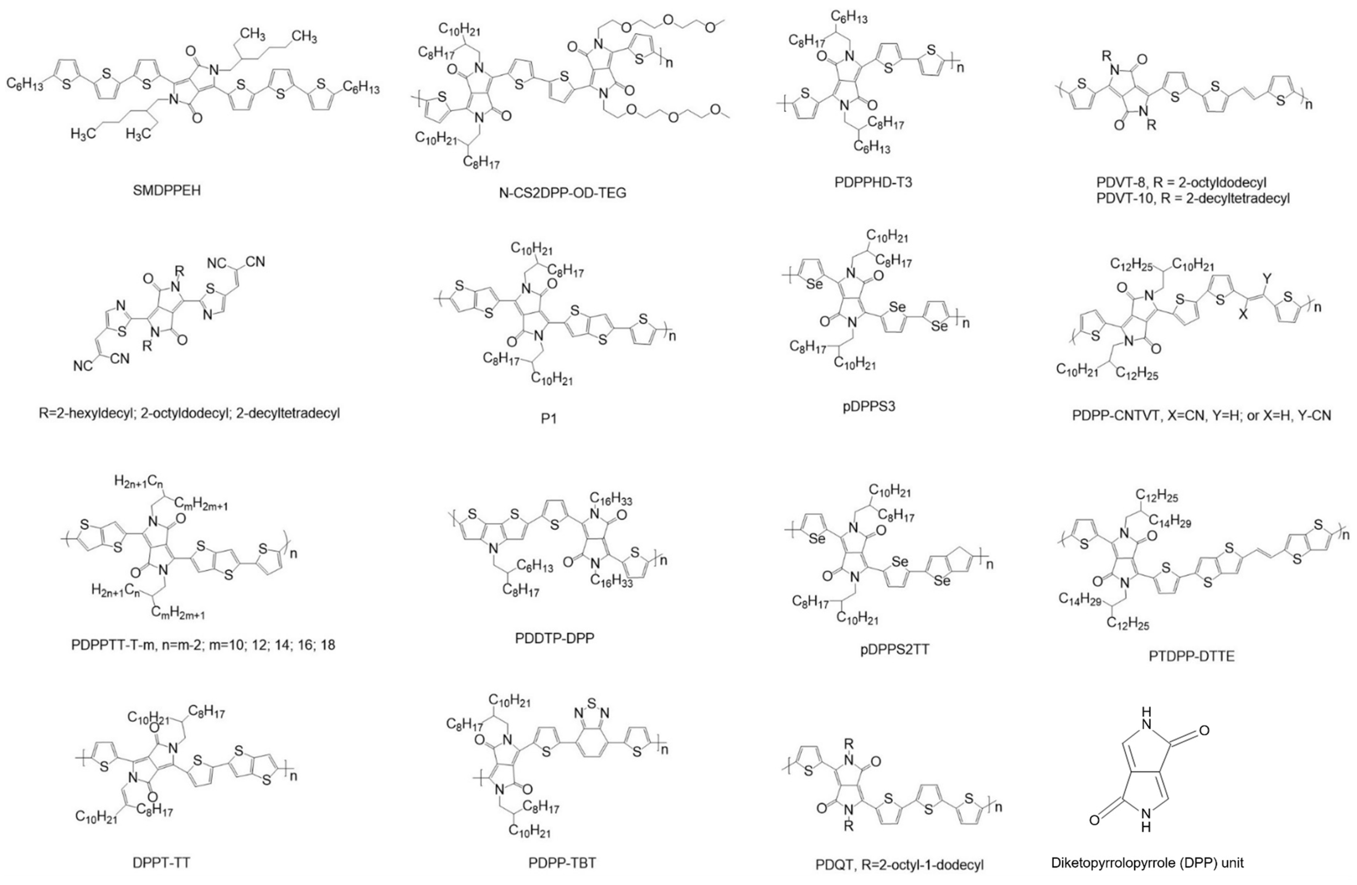
2.1. Properties of Diketopyrrolopyrrole-Based Organic Semiconductors
2.2. External Alignment of Diketopyrrolopyrrole-Based Organic Semiconductors
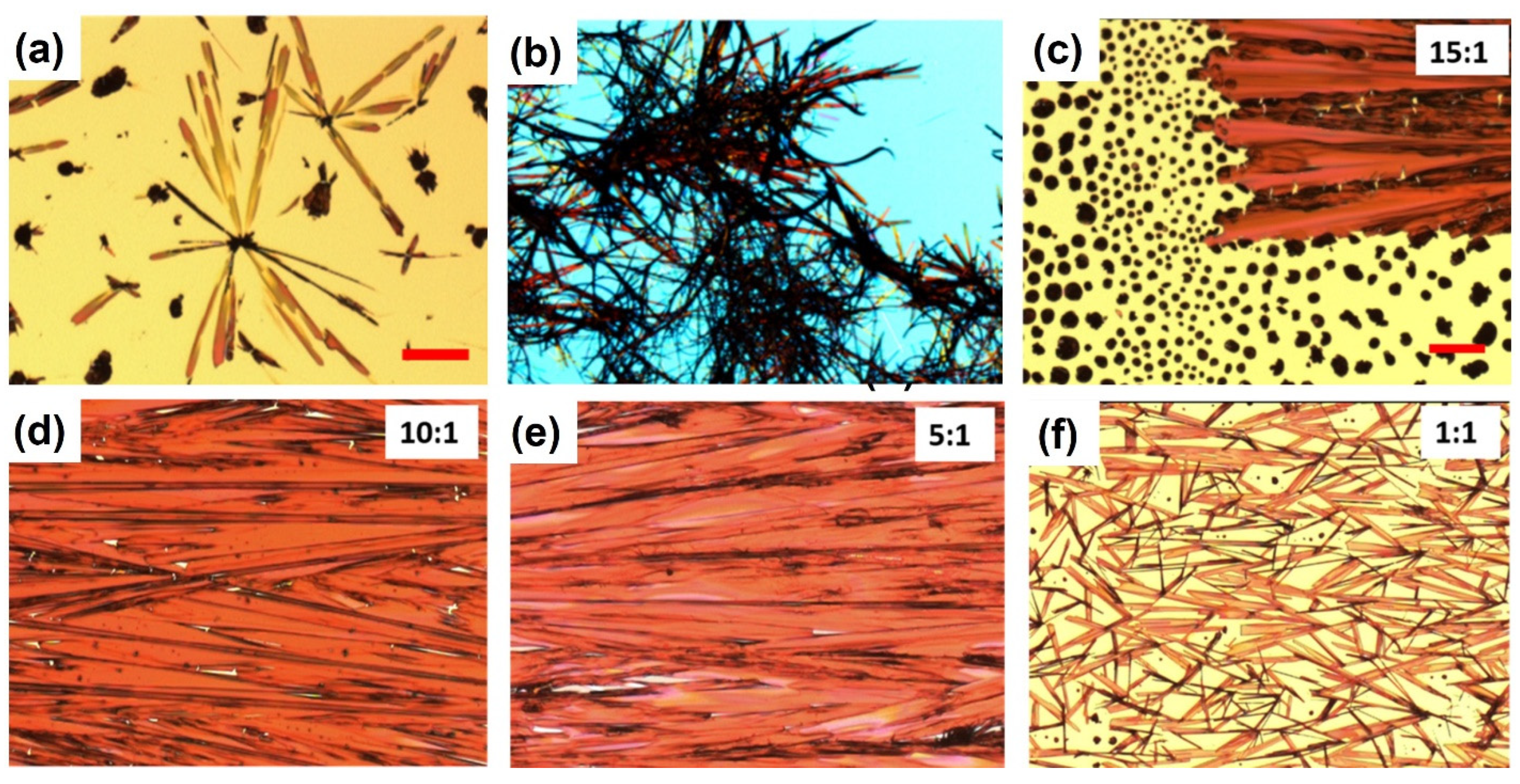
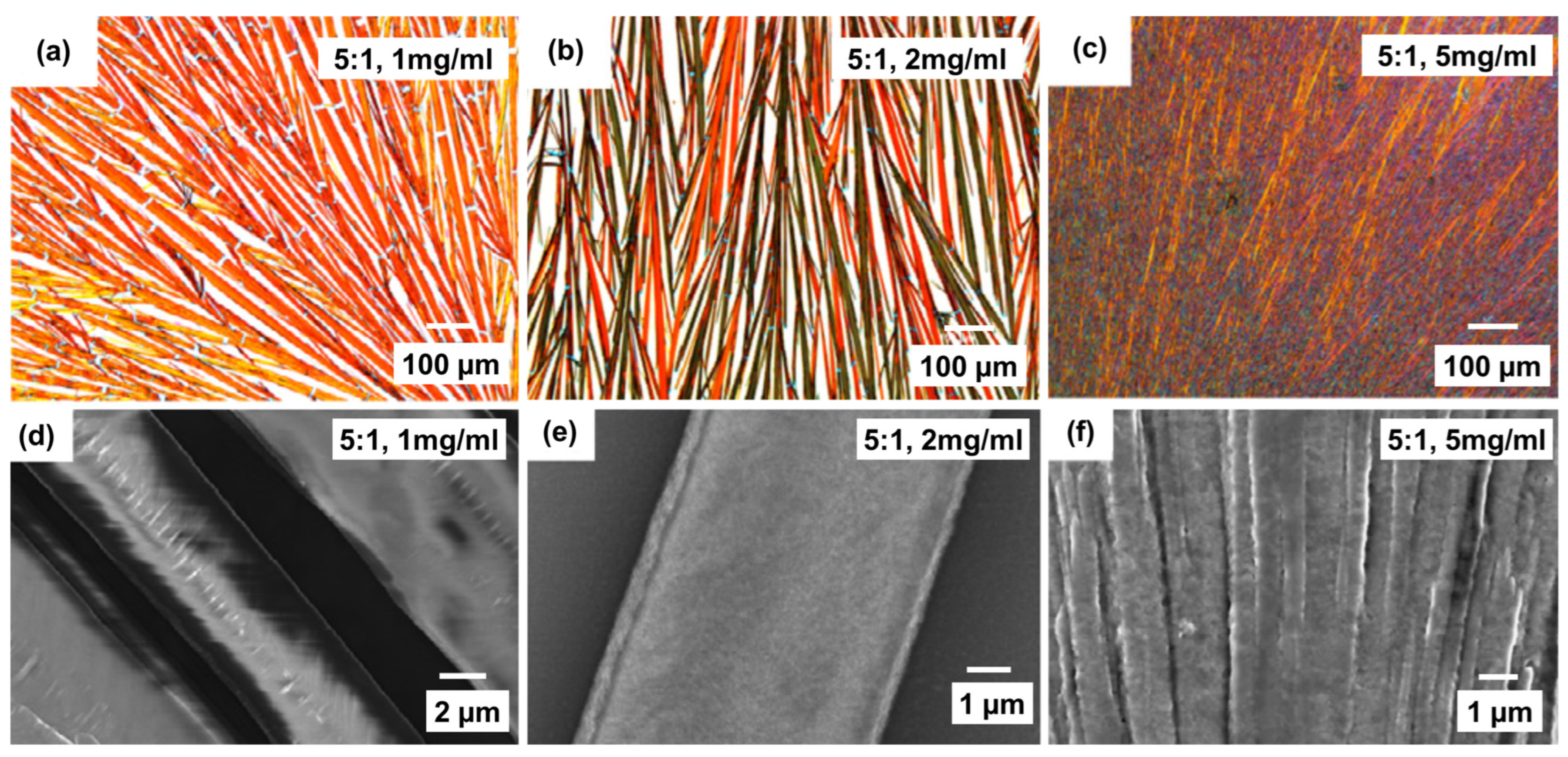
2.3. Thermal Annealing of Diketopyrrolopyrrole-Based Organic Semiconductors
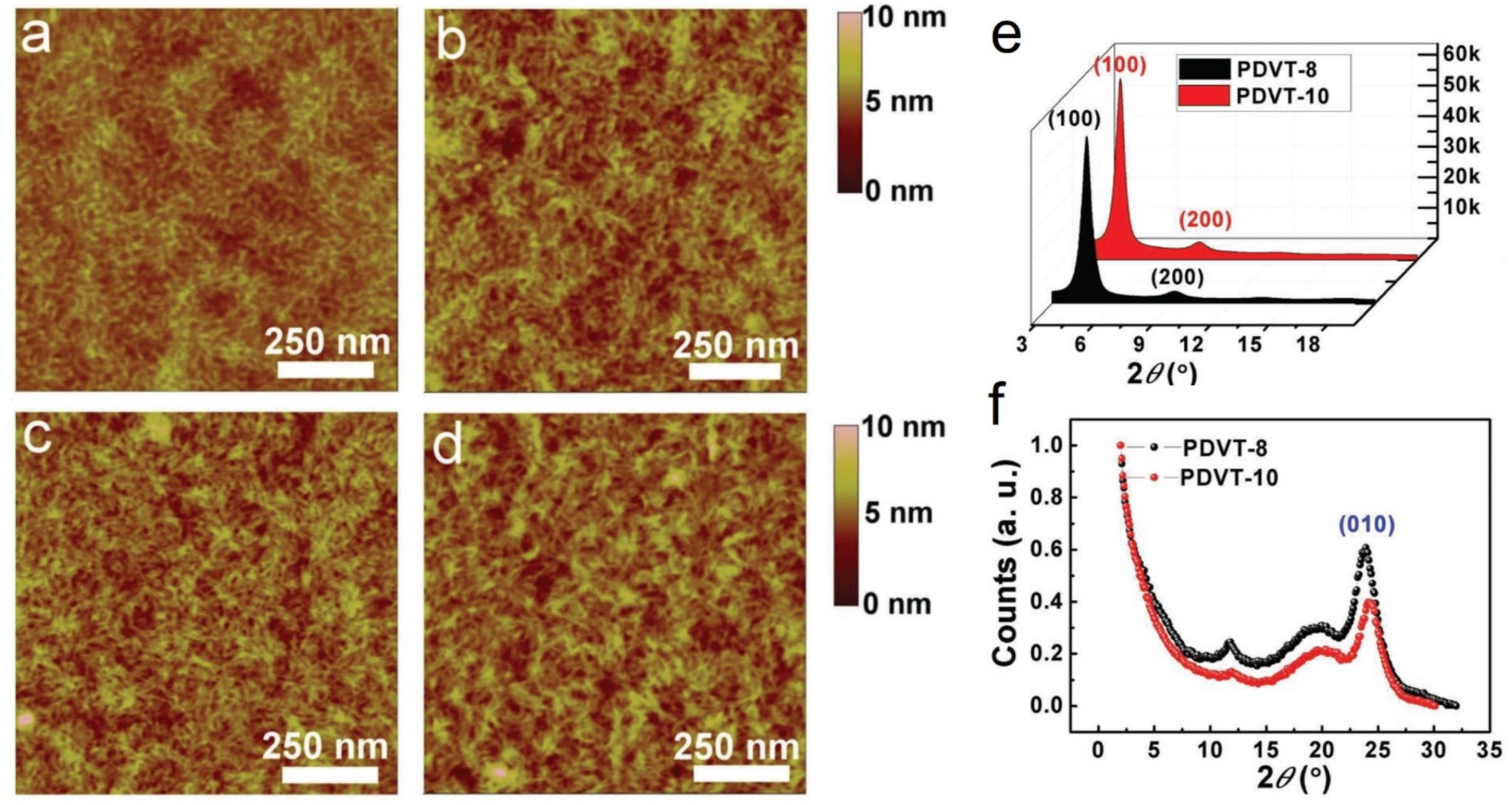
2.4. Molecular Engineering of Diketopyrrolopyrrole-Based Organic Semiconductors
2.5. Other Works on Diketopyrrolopyrrole-Based Organic Semiconductors
3. Conclusions and Outlook
Funding
Institutional Review Board Statement
Informed Consent Statement
Data Availability Statement
Conflicts of Interest
References
- Hu, P.; He, X.; Jiang, H. Greater than 10 cm2 V−1 s−1: A breakthrough of organic semiconductors for field-effect transistors. InfoMat 2021, 3, 613. [Google Scholar] [CrossRef]
- Guo, J.; Yu, B.; Zhu, F.; Yan, D. Significant improvement of 2,9-DPh-DNTT organic thin-film transistors based on organic heterojunction buffer layer. Org. Electron. 2021, 93, 106159. [Google Scholar] [CrossRef]
- Xie, P.; Liu, T.; Sun, J.; Jiang, J.; Yuan, Y.; Gao, Y.; Zhou, J.; Yang, J. Solution-processed ultra-flexible C8-BTBT organic thin-film transistors with the corrected mobility over 18 cm2/(V s). Sci. Bull. 2020, 65, 791. [Google Scholar] [CrossRef]
- Sánchez Vergara, M.E.; Santillán Esquivel, E.A.; Ballinas-Indilí, R.; Lozada-Flores, O.; Miranda-Ruvalcaba, R.; Álvarez-Toledano, C. Organic Semiconductor Devices Fabricated with Recycled Tetra Pak®-Based Electrodes and para-Quinone Methides. Coatings 2024, 14, 998. [Google Scholar] [CrossRef]
- Morab, S.; Sundaram, M.M.; Pivrikas, A. Review on Charge Carrier Transport in Inorganic and Organic Semiconductors. Coatings 2023, 13, 1657. [Google Scholar] [CrossRef]
- Orgiu, E.; Samori, P. 25th Anniversary Article: Organic Electronics Marries Photochromism: Generation of Multifunctional Interfaces, Materials, and Devices. Adv. Mater. 2014, 26, 1827. [Google Scholar] [CrossRef] [PubMed]
- Park, S.; Lee, B.; Bae, B.; Chai, J.; Lee, S.; Kim, C. Ambipolar thin-film transistors based on organic semiconductor blend. Synth. Met. 2019, 253, 40. [Google Scholar] [CrossRef]
- Lee, J.; Kwon, J.; Lim, J.; Lee, C. An Amorphous Polythiophene as a Binder Material for Organic Thin-Film Transistor Channel Applications. Mol. Cryst. Liq. Cryst. 2010, 519, 179. [Google Scholar] [CrossRef]
- Tazuhara, S.; Nagase, T.; Kobayashi, T.; Sadamitsu, Y.; Naito, H. Understanding the influence of contact resistances on short-channel high-mobility organic transistors in linear and saturation regimes. Appl. Phys. Express 2021, 14, 041010. [Google Scholar] [CrossRef]
- Tripathi, A.K.; Heinrich, M.; Siegrist, T.; Pflaum, J. Growth and Electronic Transport in 9,10-Diphenylanthracene Single Crystals—An Organic Semiconductor of High Electron and Hole Mobility. Adv. Mater. 2007, 19, 2097. [Google Scholar] [CrossRef]
- Xue, G.; Wu, J.; Fan, C.; Liu, S.; Huang, Z.; Liu, Y.; Shan, B.; Xin, H.L.; Miao, Q.; Chen, H.; et al. Boosting the electron mobility of solution-grown organic single crystals via reducing the amount of polar solvent residues. Mater. Horiz. 2016, 3, 119. [Google Scholar] [CrossRef]
- Liu, J.; Zhang, H.; Dong, H.; Meng, L.; Jiang, L.; Jiang, L.; Wang, Y.; Yu, J.; Sun, Y.; Hu, W.; et al. High mobility emissive organic semiconductor. Nat. Commun. 2015, 6, 10032. [Google Scholar] [CrossRef] [PubMed]
- Jurchescu, O.D.; Popinciuc, M.; van Wees, B.J.; Palstra, T.T.M. Interface-Controlled, High-Mobility Organic Transistors. Adv. Mater. 2007, 19, 688. [Google Scholar] [CrossRef]
- Lee, B.H.; Kim, S.; Lee, S.Y. Ammonia Gas Sensing Properties of 6,13-Bis(tri-isopropylsilyethynyl) Pentacene Based Field-Effect Transistor. Trans. Electr. Electron. Mater. 2022, 23, 182–186. [Google Scholar] [CrossRef]
- Hou, S.; Zhuang, X.; Fan, H.; Yu, J. Grain Boundary Control of Organic Semiconductors via Solvent Vapor Annealing for High-Sensitivity NO2 Detection. Sensors 2021, 21, 226. [Google Scholar] [CrossRef]
- Benavides, C.M.; Biele, M.; Schmidt, O.; Brabec, C.J.; Tedde, S.F. TIPS Pentacene as a Beneficial Interlayer for Organic Photodetectors in Imaging Applications. IEEE Trans. Electron Devices 2018, 65, 1516. [Google Scholar] [CrossRef]
- Zhao, X.; Liu, T.; Liu, H.; Wang, S.; Li, X.; Zhang, Y.; Hou, X.; Liu, Z.; Shi, W.; Dennis, T.J.S. Organic Single-Crystalline p–n Heterojunctions for High-Performance Ambipolar Field-Effect Transistors and Broadband Photodetectors. ACS Appl. Mater. Interfaces 2018, 10, 42715. [Google Scholar] [CrossRef]
- Jea, M.; Kumar, A.; Cho, H.; Yang, D.; Shim, H.; Palai, A.K.; Pyo, S. An organic microcrystal array-embedded layer: Highly directional alternating p- and n-channels for ambipolar transistors and inverters. J. Mater. Chem. C 2014, 2, 3980. [Google Scholar] [CrossRef]
- Janneck, R.; Nowack, T.S.; De Roose, F.; Ali, H.; Dehaene, W.; Heremans, P.; Genoe, J.; Rolin, C. Integration of highly crystalline C8-BTBT thin-films into simple logic gates and circuits. Org. Electron. 2019, 67, 64. [Google Scholar] [CrossRef]
- Chen, Z.; Duan, S.; Zhang, X.; Hu, W. Novel solution-processed 2D organic semiconductor crystals for high-performance OFETs. Mater. Chem. Front. 2024, 8, 2227. [Google Scholar] [CrossRef]
- Basu, R. A review on single crystal and thin film Si–Ge alloy: Growth and applications. Mater. Adv. 2022, 3, 4489. [Google Scholar] [CrossRef]
- Sun, L.; Li, T.; Zhou, J.; Li, W.; Wu, Z.; Niu, R.; Cheng, J.; Asare-Yeboah, K.; He, Z. A Green Binary Solvent Method to Control Organic Semiconductor Crystallization. ChemistrySelect 2023, 8, e202203927. [Google Scholar] [CrossRef]
- Bi, S.; Gao, B.; Han, X.; He, Z.; Metts, J.; Jiang, C.; Asare-Yeboah, K. Recent progress in printing flexible electronics: A review. Sci. China Technol. Sci. 2023, 67, 2363–2386. [Google Scholar] [CrossRef]
- Wang, Y.; Han, X.; Jin, L.; Meng, Y.; Jiang, C.; Asare-Yeboah, K.; He, Z.; Bi, S. Excitation Threshold Reduction Techniques for Organic Semiconductor Lasers: A Review. Coatings 2023, 13, 1815. [Google Scholar] [CrossRef]
- He, Z.; Zhang, Z.; Bi, S. Small-molecule additives for organic thin film transistors. J. Mater. Sci. Mater. Electron. 2019, 30, 20899. [Google Scholar] [CrossRef]
- He, Z.; Zhang, Z.; Asare-Yeboah, K.; Bi, S. Poly(α-methylstyrene) polymer and small-molecule semiconductor blend with reduced crystal misorientation for organic thin film transistors. J. Mater. Sci. Mater. Electron. 2019, 30, 14335. [Google Scholar] [CrossRef]
- Cho, S.; Lim, E. Controlling fabrication temperature of TIPS-pentacene to improve carrier properties. J. Korean Phys. Soc. 2023, 82, 91. [Google Scholar] [CrossRef]
- He, Z.; Zhang, Z.; Bi, S. Long-range crystal alignment with polymer additive for organic thin film transistors. J. Polym. Res. 2019, 26, 173. [Google Scholar] [CrossRef]
- Zhang, S.; Talnack, F.; Jousselin-Oba, T.; Bhat, V.; Wu, Y.; Lei, Y.; Tomo, Y.; Gong, H.; Michalek, L.; Zhong, D.; et al. Shear-aligned large-area organic semiconductor crystals through extended π–π interaction. J. Mater. Chem. C 2023, 11, 8992. [Google Scholar] [CrossRef]
- He, Z.; Chen, J.; Li, D. Crystal alignment for high performance organic electronics devices. J. Vac. Sci. Technol. A 2019, 37, 040801. [Google Scholar] [CrossRef]
- Tamayo, A.; Hofer, S.; Salzillo, T.; Ruzié, C.; Schweicher, G.; Resel, R.; Mas-Torrent, M. Mobility anisotropy in the herringbone structure of asymmetric Ph-BTBT-10 in solution sheared thin film transistors. J. Mater. Chem. C 2021, 9, 7186. [Google Scholar] [CrossRef]
- He, Z.; Zhang, Z.; Bi, S.; Asare-Yeboah, K.; Chen, J. Ultra-low misorientation angle in small-molecule semiconductor/polyethylene oxide blends for organic thin film transistors. J. Polym. Res. 2020, 27, 75. [Google Scholar] [CrossRef]
- Bai, J.; Jiang, Y.; Wang, Z.; Sui, Y.; Deng, Y.; Han, Y.; Geng, Y. Bar-Coated Organic Thin-Film Transistors with Reliable Electron Mobility Approaching 10 cm2 V−1 s−1. Adv. Electron. Mater. 2020, 6, 1901002. [Google Scholar] [CrossRef]
- He, Z.; Zhang, Z.; Bi, S. Polyacrylate Polymer Assisted Crystallization: Improved Charge Transport and Performance Consistency for Solution-Processable Small-Molecule Semiconductor Based Organic Thin Film Transistors. J. Sci. Adv. Mater. Devices 2019, 4, 467. [Google Scholar] [CrossRef]
- Kim, N.-K.; Jang, S.-Y.; Pace, G.; Caironi, M.; Park, W.-T.; Khim, D.; Kim, J.; Kim, D.-Y.; Noh, Y.-Y. High-Performance Organic Field-Effect Transistors with Directionally Aligned Conjugated Polymer Film Deposited from Pre-Aggregated Solution. Chem. Mater. 2015, 27, 8345. [Google Scholar] [CrossRef]
- Diao, Y.; Shaw, L.; Bao, Z.A.; Mannsfeld, S.C.B. Morphology control strategies for solution-processed organic semiconductor thin films. Energy Environ. Sci. 2014, 7, 2145. [Google Scholar] [CrossRef]
- He, Z.; Bi, S.; Asare-Yeboah, K.; Zhang, Z. Phase segregation effect on TIPS pentacene crystallization and morphology for organic thin film transistors. J. Mater. Sci. Mater. Electron. 2020, 31, 4503. [Google Scholar] [CrossRef]
- Chen, J.H.; Martin, D.C.; Anthony, J.E. Morphology and molecular orientation of thin-film bis(triisopropylsilylethynyl) pentacene. J. Mater. Res. 2007, 22, 1701. [Google Scholar] [CrossRef]
- He, Z.; Lopez, N.; Chi, X.; Li, D. Solution-based 5,6,11,12-tetrachlorotetracene crystal growth for high-performance organic thin film transistors. Org. Electron. 2015, 22, 191. [Google Scholar] [CrossRef]
- Chen, J.H.; Anthony, J.E.; Martin, D.C. Crystallographic cracking during a thermally-induced solid-state phase transition in TIPS pentacene. Abstr. Pap. Am. Chem. Soc. 2005, 230, 309. [Google Scholar]
- He, Z.; Zhang, Z.; Bi, S.; Chen, J. Tuning charge transport in organic semiconductors with nanoparticles and hexamethyldisilazane. J. Nanopart. Res. 2021, 23, 5. [Google Scholar] [CrossRef]
- Chi, X.L.; Li, D.W.; Zhang, H.Q.; Chen, Y.S.; Garcia, V.; Garcia, C.; Siegrist, T. 5,6,11,12-Tetrachlorotetracene, a tetracene derivative with pi-stacking structure: The synthesis, crystal structure and transistor properties. Org. Electron. 2008, 9, 234. [Google Scholar] [CrossRef]
- Yagodkin, E.; Xia, Y.; Kalihari, V.; Frisbie, C.D.; Douglas, C.J. Synthesis, Solid State Properties, and Semiconductor Measurements of 5,6,11,12-Tetrachlorotetracene. J. Phys. Chem. C 2009, 113, 16544. [Google Scholar] [CrossRef]
- Hwang, D.K.; Fuentes-Hernandez, C.; Kim, J.B.; Potscavage, W.J.; Kippelen, B. Flexible and stable solution-processed organic field-effect transistors. Org. Electron. 2011, 12, 1108. [Google Scholar] [CrossRef]
- James, D.T.; Kjellander, B.K.C.; Smaal, W.T.T.; Gelinck, G.H.; Combe, C.; McCulloch, I.; Wilson, R.; Burroughes, J.H.; Bradley, D.D.C.; Kim, J.S. Thin-Film Morphology of Inkjet-Printed Single-Droplet Organic Transistors Using Polarized Raman Spectroscopy: Effect of Blending TIPS-Pentacene with Insulating Polymer. Acs Nano 2011, 5, 9824. [Google Scholar] [CrossRef]
- Rogowski, R.Z.; Dzwilewski, A.; Kemerink, M.; Darhuber, A.A. Solution Processing of Semiconducting Organic Molecules for Tailored Charge Transport Properties. J. Phys. Chem. C 2011, 115, 11758. [Google Scholar] [CrossRef]
- Li, Y.; Liu, C.; Kumatani, A.; Darmawan, P.; Minari, T.; Tsukagoshi, K. Patterning solution-processed organic single-crystal transistors with high device performance. AIP Adv. 2011, 1, 022149. [Google Scholar] [CrossRef]
- Chen, J.H.; Tee, C.K.; Shtein, M.; Martin, D.C.; Anthony, J. Controlled solution deposition and systematic study of charge-transport anisotropy in single crystal and single-crystal textured TIPS pentacene thin films. Org. Electron. 2009, 10, 696. [Google Scholar] [CrossRef]
- He, Z.; Asare-Yeboah, K.; Zhang, Z.; Bi, S. Manipulate organic crystal morphology and charge transport. Org. Electron. 2022, 103, 106448. [Google Scholar] [CrossRef]
- Briseno, A.L.; Mannsfeld, S.C.B.; Ling, M.M.; Liu, S.H.; Tseng, R.J.; Reese, C.; Roberts, M.E.; Yang, Y.; Wudl, F.; Bao, Z.N. Patterning organic single-crystal transistor arrays. Nature 2006, 444, 913. [Google Scholar] [CrossRef]
- Kuribara, K.; Nobeshima, T.; Takei, A.; Kodzasa, T.; Uemura, S.; Yoshida, M. Wettability control with self-assembler patterning for printed electronics. Jpn. J. Appl. Phys. 2019, 58, 041002. [Google Scholar] [CrossRef]
- Chen, Z.; Duan, S.; Zhang, X.; Geng, B.; Xiao, Y.; Jie, J.; Dong, H.; Li, L.; Hu, W. Organic Semiconductor Crystal Engineering for High-Resolution Layer-Controlled 2D Crystal Arrays. Adv. Mater. 2021, 34, 2104166. [Google Scholar] [CrossRef]
- Li, W.; Li, L.; Sun, Q.; Liu, X.; Kanehara, M.; Nakayama, T.; Jiu, J.; Sakamoto, K.; Minari, T. Direct fabrication of high-resolution and high-performance flexible electronics via surface-activation-localized electroless plating. Chem. Eng. J. 2021, 416, 127644. [Google Scholar] [CrossRef]
- Kolodziejczyk, B.; Winther-Jensen, O.; Pereira, B.A.; Nair, S.S.; Winther-Jensen, B. Patterning of conducting layers on breathable substrates using laser engraving for gas sensors. J. Appl. Polym. Sci. 2015, 132, 42359. [Google Scholar] [CrossRef]
- Jo, P.S.; Duong, D.T.; Park, J.; Sinclair, R.; Salleo, A. Control of Rubrene Polymorphs via Polymer Binders: Applications in Organic Field-Effect Transistors. Chem. Mater. 2015, 27, 3979. [Google Scholar] [CrossRef]
- Wang, B.; Zhu, T.; Huang, L.; Tam, T.L.D.; Cui, Z.; Ding, J.; Chi, L. Addressable growth of oriented organic semiconductor ultra-thin films on hydrophobic surface by direct dip-coating. Org. Electron. 2015, 24, 170. [Google Scholar] [CrossRef]
- Meng, Q.; Zhang, F.; Zang, Y.; Huang, D.; Zou, Y.; Liu, J.; Zhao, G.; Wang, Z.; Ji, D.; Di, C.-A.; et al. Solution-sheared ultrathin films for highly-sensitive ammonia detection using organic thin-film transistors. J. Mater. Chem. C 2014, 2, 1264. [Google Scholar] [CrossRef]
- Kim, K.; Nam, K.; Li, X.; Lee, D.Y.; Kim, S.H. Programmed Design of Highly Crystalline Organic Semiconductor Patterns with Uniaxial Alignment via Blade Coating for High-Performance Organic Field-Effect. ACS Appl. Mater. Interfaces 2019, 11, 42403. [Google Scholar] [CrossRef] [PubMed]
- Leonardi, F.; Zhang, Q.; Kim, Y.-H.; Mas-Torrent, M. Solution-sheared thin films of a donor-acceptor random copolymerpolystyrene blend as active material in field-effect transistors. Mater. Sci. Semicond. Process. 2019, 93, 105. [Google Scholar] [CrossRef]
- Kwon, H.-J.; Kim, K.; An, T.K.; Kim, S.H.; Park, C.E. Effect of lateral confinement on crystallization behavior of a small-molecule semiconductor during capillary force lithography for use in high-performance OFETs. J. Ind. Eng. Chem. 2019, 75, 187. [Google Scholar] [CrossRef]
- Park, Y.; Park, J.; Cho, S.; Sung, M.M. Large-area single-crystal organic patterned thin films by vertically confined lateral crystal growth via capillary force lithography. Appl. Surf. Sci. 2019, 494, 1023. [Google Scholar] [CrossRef]
- Ma, X.; Liu, Q.; Xu, D.; Zhu, Y.; Kim, S.; Cui, Y.; Zhong, L.; Liu, M. Capillary-Force-Assisted Clean-Stamp Transfer of Two-Dimensional Materials. Nano Lett. 2017, 17, 6961. [Google Scholar] [CrossRef] [PubMed]
- Schweicher, G.; Liu, G.; Fastré, P.; Resel, R.; Abbas, M.; Wantz, G.; Geerts, Y.H. Directional crystallization of C8-BTBT-C8 thin films in a temperature gradient. Mater. Chem. Front. 2021, 5, 249. [Google Scholar] [CrossRef]
- Kneppe, D.; Talnack, F.; Boroujeni, B.K.; Teixeira da Rocha, C.; Höppner, M.; Tahn, A.; Mannsfeld, S.C.B.; Ellinger, F.; Leo, K.; Kleemann, H. Solution-processed pseudo-vertical organic transistors based on TIPS-pentacene. Mater. Today Energy 2021, 21, 100697. [Google Scholar] [CrossRef]
- Yang, Z.; Lin, S.; Liu, J.; Zheng, K.; Lu, G.; Ye, B.; Huang, J.; Zhang, Y.; Ye, Y.; Guo, T.; et al. High performance phototransistors with organic/quantum dot composite materials channels. Org. Electron. 2020, 78, 105565. [Google Scholar] [CrossRef]
- Najafi-Ashtiani, F. Low temperature processing of BaTiO3-PMMA-PVP hybrid films as transparent dielectric gate. J. Mater. Sci.-Mater. Electron. 2019, 30, 7087. [Google Scholar] [CrossRef]
- Haq, Y.-U.; Ullah, R.; Mazhar, S.; Khattak, R.; Qarni, A.A.; Haq, Z.-U.; Amin, S. Synthesis and characterization of 2D MXene: Device fabrication for humidity sensing. J. Sci. Adv. Mater. Devices 2021, 7, 100390. [Google Scholar] [CrossRef]
- Powell, D.; Campbell, E.V.; Flannery, L.; Ogle, J.; Soss, S.E.; Whittaker-Brooks, L. Steric hindrance dependence on the spin and morphology properties of highly oriented self-doped organic small molecule thin films. Mater. Adv. 2021, 2, 356. [Google Scholar] [CrossRef]
- Mohammed, H.Y.; Farea, M.A.; Sayyad, P.W.; Ingle, N.N.; Al-Gahouari, T.; Mahadik, M.M.; Bodkhe, G.A.; Shirsat, S.M.; Shirsat, M.D. Selective and sensitive chemiresistive sensors based on polyaniline/graphene oxide nanocomposite: A cost-effective approach. J. Sci. Adv. Mater. Devices 2021, 7, 100391. [Google Scholar] [CrossRef]
- Yang, Z.; Lin, S.; Liu, J.; Zheng, K.; Lu, G.; Ye, B.; Huang, J.; Zhang, Y.; Ye, Y.; Guo, T.; et al. Sharp phase-separated interface of 6, 13-bis (triisopropylsilylethynyl) pentacene/polystyrene blend films prepared by electrostatic spray deposition. Org. Electron. 2020, 78, 206. [Google Scholar]
- Park, M.; Cho, W.; Lee, G.; Hong, S.C.; Kim, M.C.; Yoon, J.; Ahn, N.; Choi, M. Highly Reproducible Large-Area Perovskite Solar Cell Fabrication via Continuous Megasonic Spray Coating of CH3NH3PbI3. Small 2019, 15, 1804005. [Google Scholar] [CrossRef]
- Koutsiaki, C.; Kaimakamis, T.; Zachariadis, A.; Papamichail, A.; Kamaraki, C.; Fachouri, S.; Gravalidis, C.; Laskarakis, A.; Logothetidis, S. Efficient combination of Roll-to-Roll compatible techniques towards the large area deposition of a polymer dielectric film and the solution-processing of an organic semiconductor for the field-effect transistors fabrication on plastic substrate. Org. Electron. 2019, 73, 231. [Google Scholar] [CrossRef]
- Teisala, H.; Tuominen, M.; Stepien, M.; Haapanen, J.; Makela, J.M.; Saarinen, J.J.; Toivakka, M.; Kuusipalo, J. Wettability conversion on the liquid flame spray generated superhydrophobic TiO2 nanoparticle coating on paper and board by photocatalytic decomposition of spontaneously accumulated carbonaceous overlayer. Cellulose 2013, 20, 391. [Google Scholar] [CrossRef]
- Hwang, J.Y.; Kim, D.; Jang, H.; Lee, S.-Y.; Joo, Y.-C. Thermal and Electrical Properties Depending on the Bonding Structure of Amorphous Carbon Thin Films. Electron. Mater. Lett. 2024, 20, 648–656. [Google Scholar] [CrossRef]
- Kim, J.W.; An, J.G.; Oh, G.H.; Park, J.H.; Kim, T. Improved Performance of Transparent MoS2 Thin-Film Transistor with IZO Electrodes by Air Thermal Annealing. Electron. Mater. Lett. 2024, 20, 225. [Google Scholar] [CrossRef]
- O’Connor, B.T.; Reid, O.G.; Zhang, X.; Kline, R.J.; Richter, L.J.; Gundlach, D.J.; DeLongchamp, D.M.; Toney, M.F.; Kopidakis, N.; Rumbles, G. Morphological Origin of Charge Transport Anisotropy in Aligned Polythiophene Thin Films. Adv. Funct. Mater. 2014, 24, 3422. [Google Scholar] [CrossRef]
- Du, C.; Wang, W.C.; Li, L.Q.; Fuchs, H.; Chi, L.F. Growth of rubrene crystalline thin films using thermal annealing on DPPC LB monolayer. Org. Electron. 2013, 14, 2534. [Google Scholar] [CrossRef]
- Li, Y.; Sonar, P.; Singh, S.P.; Soh, M.S.; van Meurs, M.; Tan, J. Annealing-Free High-Mobility Diketopyrrolopyrrole−Quaterthiophene Copolymer for Solution-Processed Organic Thin Film Transistors. J. Am. Chem. Soc. 2011, 133, 2198. [Google Scholar] [CrossRef]
- Shin, J.; Hong, T.R.; Lee, T.W.; Kim, A.; Kim, Y.H.; Cho, M.J.; Choi, D.H. Template-Guided Solution-Shearing Method for Enhanced Charge Carrier Mobility in Diketopyrrolopyrrole-Based Polymer Field-Effect Transistors. Adv. Mater. 2014, 26, 6031. [Google Scholar] [CrossRef]
- Chen, H.; Guo, Y.; Yu, G.; Zhao, Y.; Zhang, J.; Gao, D.; Liu, H.; Liu, Y. Highly π-Extended Copolymers with Diketopyrrolopyrrole Moieties for High-Performance Field-Effect Transistors. Adv. Mater. 2012, 24, 4618. [Google Scholar] [CrossRef]
- Yun, H.-J.; Kang, S.-J.; Xu, Y.; Kim, S.O.; Kim, Y.-H.; Noh, Y.-Y.; Kwon, S.-K. Dramatic Inversion of Charge Polarity in Diketopyrrolopyrrole-Based Organic Field-Effect Transistors via a Simple Nitrile Group Substitution. Adv. Mater. 2014, 26, 7300. [Google Scholar] [CrossRef] [PubMed]
- Chen, J.H.; Tee, C.K.; Yang, J.Y.; Shaw, C.; Shtein, M.; Anthony, J.; Martin, D.C. Thermal and mechanical cracking in bis(triisopropylsilyiethnyl) pentacene thin films. J. Polym. Sci. Part B-Polym. Phys. 2006, 44, 3631. [Google Scholar] [CrossRef]
- He, Z.; Li, D.; Hensley, D.K.; Rondinone, A.J.; Chen, J. Switching phase separation mode by varying the hydrophobicity of polymer additives in solution-processed semiconducting small-molecule/polymer blends. Appl. Phys. Lett. 2013, 103, 113301. [Google Scholar] [CrossRef]
- He, Z.; Chen, J.; Sun, Z.; Szulczewski, G.; Li, D. Air-flow navigated crystal growth for TIPS pentacene-based organic thin-film transistors. Org. Electron. 2012, 13, 1819. [Google Scholar] [CrossRef]
- He, Z.; Xiao, K.; Durant, W.; Hensley, D.K.; Anthony, J.E.; Hong, K.; Kilbey, S.M., II; Chen, J.; Li, D. Enhanced Performance Consistency in Nanoparticle/TIPS Pentacene-Based Organic Thin Film Transistors. Adv. Funct. Mater. 2011, 21, 3617. [Google Scholar] [CrossRef]
- Diao, Y.; Tee, B.C.K.; Giri, G.; Xu, J.; Kim, D.H.; Becerril, H.A.; Stoltenberg, R.M.; Lee, T.H.; Xue, G.; Mannsfeld, S.C.B.; et al. Solution coating of large-area organic semiconductor thin films with aligned single-crystalline domains. Nat. Mater. 2013, 12, 665. [Google Scholar] [CrossRef] [PubMed]
- Yuan, Y.B.; Giri, G.; Ayzner, A.L.; Zoombelt, A.P.; Mannsfeld, S.C.B.; Chen, J.H.; Nordlund, D.; Toney, M.F.; Huang, J.S.; Bao, Z.N. Ultra-high mobility transparent organic thin film transistors grown by an off-centre spin-coating method. Nat. Commun. 2014, 5, 3005. [Google Scholar] [CrossRef] [PubMed]
- Zhang, Z.; Asare-Yeboah, K.; Bi, S.; He, Z. Poly(α-methyl styrene) polymer additive for organic thin film transistors. J. Mater. Sci. Mater. Electron. 2022, 33, 1101. [Google Scholar] [CrossRef]
- He, Z.; Zhang, Z.; Asare-Yeboah, K.; Bi, S. Solvent Exchange in Controlling Semiconductor Morphology. Electron. Mater. Lett. 2022, 18, 501. [Google Scholar] [CrossRef]
- Coropceanu, V.; Cornil, J.; da Silva Filho, D.A.; Olivier, Y.; Silbey, R.; Brédas, J.-L. Charge Transport in Organic Semiconductors. Chem. Rev. 2007, 107, 926. [Google Scholar] [CrossRef]
- He, Z.; Zhang, Z.; Bi, S. Nanoparticles for organic electronics applications. Mater. Res. Express 2020, 7, 012004. [Google Scholar] [CrossRef]
- Bronstein, H.; Nielsen, C.B.; Schroeder, B.C.; McCulloch, I. The role of chemical design in the performance of organic semiconductors. Nat. Rev. Chem. 2020, 4, 66. [Google Scholar] [CrossRef] [PubMed]
- He, Z.; Zhang, Z.; Bi, S. Tailoring the molecular weight of polymer additives for organic semiconductors. Mater. Adv. 2022, 3, 1953. [Google Scholar] [CrossRef]
- Virkar, A.A.; Mannsfeld, S.; Bao, Z.; Stingelin, N. Organic Semiconductor Growth and Morphology Considerations for Organic Thin-Film Transistors. Adv. Mater. 2010, 22, 3857. [Google Scholar] [CrossRef] [PubMed]
- He, Z.; Chen, J.; Li, D. Polymer Additive Controlled Morphology for High Performance Organic Thin Film Transistors. Soft Matter 2019, 15, 5790. [Google Scholar] [CrossRef] [PubMed]
- Wang, C.; Dong, H.; Jiang, L.; Hu, W. Organic semiconductor crystals. Chem. Soc. Rev. 2018, 47, 422. [Google Scholar] [CrossRef]
- Yue, H.; Guo, M.; Ming, S.; Du, H.; Zhao, J.; Zhang, J. Fine-tuning the color hue of the solution-processable electrochromic copolymers based on the diketopyrrolopyrrole, benzodithiophene and dithienosilole units. Colloids Surf. A Physicochem. Eng. Asp. 2024, 684, 133094. [Google Scholar] [CrossRef]
- Jiang, W.; Liu, Z.; Zhu, D.; Zheng, W.; Chen, L.; Zhang, X.; Zhang, G.; Yi, Y.; Jiang, L.; Zhang, D. New Synthetic Approaches to N-Aryl and π-Expanded Diketopyrrolopyrroles as New Building Blocks for Organic Optoelectronic Materials. Angew. Chem. Int. Ed. 2021, 60, 10700. [Google Scholar] [CrossRef]
- Leenaers, P.J.; van Eersel, H.; Li, J.; Wienk, M.M.; Janssen, R.A.J. Influence of Regioregularity on the Optoelectronic Properties of Conjugated Diketopyrrolopyrrole Polymers Comprising Asymmetric Monomers. Macromolecules 2020, 53, 7749. [Google Scholar] [CrossRef]
- Shen, T.; Wu, Z.; Jiang, Z.; Yan, D.; Zhao, Y.; Wang, Y.; Liu, Y. Elucidating the effects of the sidechain substitution direction on the optoelectronic properties of isomeric diketopyrrolopyrrole-based conjugated polymers for near-infrared organic phototransistors. J. Mater. Chem. C 2024, 12, 489. [Google Scholar] [CrossRef]
- Adnan, M.; Kashif, M.; Irshad, Z.; Hussain, R.; Darwish, H.W.; Lim, J. Advancing optoelectronic characteristics of Diketopyrrolopyrrole-Based molecules as donors for organic and as hole transporting materials for perovskite solar cells. Spectrochim. Acta Part A Mol. Biomol. Spectrosc. 2024, 320, 124615. [Google Scholar] [CrossRef] [PubMed]
- Farnum, D.G.; Mehta, G.; Moore, G.G.I.; Siegal, F.P. Attempted reformatskii reaction of benzonitrile, 1,4-diketo-3,6-diphenylpyrrolo [3,4-C]pyrrole. A lactam analogue of pentalene. Tetrahedron Lett. 1974, 15, 2549. [Google Scholar] [CrossRef]
- Iqbal, A.; Jost, M.; Kirchmayr, R.; Pfenninger, J.; Rochat, A.; Wallquist, O. The synthesis and properties of 1,4-diketo-pyrrolo [3,4-C]pyrroles. Bull. Sociétés Chim. Belg. 1988, 97, 615. [Google Scholar] [CrossRef]
- Yiu, A.T.; Beaujuge, P.M.; Lee, O.P.; Woo, C.H.; Toney, M.F.; Fréchet, J.M.J. Side-Chain Tunability of Furan-Containing Low-Band-Gap Polymers Provides Control of Structural Order in Efficient Solar Cells. J. Am. Chem. Soc. 2012, 134, 2180. [Google Scholar] [CrossRef]
- Shaikh, S.A.L.; Birajdar, S.S.; Ambore, S.D.; Puyad, A.L.; Vijayanand, P.; Bhosale, S.V.; Bhosale, S.V. A minireview on diketopyrrolopyrrole chemistry: Historical perspective and recent developments. Results Chem. 2022, 4, 100473. [Google Scholar] [CrossRef]
- Luo, N.; Zhang, G.; Liu, Z. Keep glowing and going: Recent progress in diketopyrrolopyrrole synthesis towards organic optoelectronic materials. Org. Chem. Front. 2021, 8, 4560. [Google Scholar] [CrossRef]
- Tang, M.; Wu, S.; Xing, W.; Shen, H.; Xiang, L.; Liang, Y.; Xu, W.; Zhu, D. Diketopyrrolopyrrole based small molecular semiconductors containing thiazole units for solution-processed n-channel thin-film transistors. Dyes Pigments 2019, 163, 707. [Google Scholar] [CrossRef]
- Kwon, J.-H.; Kim, M.-H.; Bae, J.-H. A review on diverse streams of interface engineering for organic thin-film transistors. J. Mater. Chem. C 2024, 12, 29. [Google Scholar] [CrossRef]
- Song, J.; Liu, H.; Zhao, Z.; Lin, P.; Yan, F. Flexible Organic Transistors for Biosensing: Devices and Applications. Adv. Mater. 2024, 36, 2300034. [Google Scholar] [CrossRef]
- Shin, H.; Kim, D.; Park, J.; Kim, D.Y. Improving Photosensitivity and Transparency in Organic Phototransistor with Blending Insulating Polymers. Micromachines 2023, 14, 620. [Google Scholar] [CrossRef]
- Jain, S.K.; Joshi, A.M.; Bharti, D. Effect of Temperature on Performance Characteristics with Varying Defect States Parameters in TIPS-pentacene Based OTFTs on n++ Silicon Substrate. Silicon 2023, 15, 6397. [Google Scholar] [CrossRef]
- He, Z.; Chen, J.; Keum, J.K.; Szulczewski, G.; Li, D. Improving performance of TIPS pentacene-based organic thin film transistors with small-molecule additives. Org. Electron. 2014, 15, 150. [Google Scholar] [CrossRef]
- Chen, J.; Shao, M.; Xiao, K.; He, Z.; Li, D.; Lokitz, B.S.; Hensley, D.K.; Kilbey, S.M., II; Anthony, J.E.; Keum, J.K.; et al. Conjugated Polymer-Mediated Polymorphism of a High Performance, Small-Molecule Organic Semiconductor with Tuned Intermolecular Interactions, Enhanced Long-Range Order, and Charge Transport. Chem. Mater. 2013, 25, 4378. [Google Scholar] [CrossRef]
- Lewińska, G. Ternary Organic Solar Cells—Simulation–Optimization Approach. Electron. Mater. Lett. 2024, 20, 440. [Google Scholar] [CrossRef]
- Corzo, D.; Rosas-Villalva, D.; C, A.; Tostado-Blázquez, G.; Alexandre, E.B.; Hernandez, L.H.; Han, J.; Xu, H.; Babics, M.; De Wolf, S.; et al. High-performing organic electronics using terpene green solvents from renewable feedstocks. Nat. Energy 2023, 8, 62. [Google Scholar] [CrossRef]
- Ayub, A.; Ans, M.; Gul, S.; Shawky, A.M.; Ayub, K.; Iqbal, J.; Hashmi, M.A.; Lakhani, A. Toward High-Performance Quinoxaline Based Non-fullerene Small Molecule Acceptors for Organic Solar Cells. Electron. Mater. Lett. 2023, 19, 38. [Google Scholar] [CrossRef]
- Xu, X.; Zhao, Y.; Liu, Y. Wearable Electronics Based on Stretchable Organic Semiconductors. Small 2023, 19, 2206309. [Google Scholar] [CrossRef]
- Aderne, R.E.; Borges, B.G.A.L.; Ávila, H.C.; von Kieseritzky, F.; Hellberg, J.; Koehler, M.; Cremona, M.; Roman, L.S.; Araujo, C.M.; Rocco, M.L.M.; et al. On the energy gap determination of organic optoelectronic materials: The case of porphyrin derivatives. Mater. Adv. 2022, 3, 1791. [Google Scholar] [CrossRef]
- Sani, M.J. Theoretical survey on the electronic, linear and nonlinear optical properties of substituted benzenes and polycondensed π-systems. A density functional theory study. Comput. Theor. Chem. 2023, 1223, 114100. [Google Scholar] [CrossRef]
- Huang, J.; Yu, G. Recent progress in quinoidal semiconducting polymers: Structural evolution and insight. Mater. Chem. Front. 2021, 5, 76. [Google Scholar] [CrossRef]
- Liu, Q.; Bottle, S.E.; Sonar, P. Developments of Diketopyrrolopyrrole-Dye-Based Organic Semiconductors for a Wide Range of Applications in Electronics. Adv. Mater. 2020, 32, 1903882. [Google Scholar] [CrossRef] [PubMed]
- Grzybowski, M.; Gryko, D.T. Diketopyrrolopyrroles: Synthesis, Reactivity, and Optical Properties. Adv. Opt. Mater. 2015, 3, 280. [Google Scholar] [CrossRef]
- Addanki Tirumala, R.T.; Khatri, N.; Ramakrishnan, S.B.; Mohammadparast, F.; Khan, M.T.; Tan, S.; Wagle, P.; Puri, S.; McIlroy, D.N.; Kalkan, A.K.; et al. Tuning Catalytic Activity and Selectivity in Photocatalysis on Mie-Resonant Cuprous Oxide Particles: Distinguishing Electromagnetic Field Enhancement Effect from the Heating Effect. ACS Sustain. Chem. Eng. 2023, 11, 15931. [Google Scholar] [CrossRef]
- Tirumala, R.T.A.; Gyawali, S.; Wheeler, A.; Ramakrishnan, S.B.; Sooriyagoda, R.; Mohammadparast, F.; Khatri, N.; Tan, S.; Kalkan, A.K.; Bristow, A.D.; et al. Structure–Property–Performance Relationships of Cuprous Oxide Nanostructures for Dielectric Mie Resonance-Enhanced Photocatalysis. ACS Catal. 2022, 12, 7975. [Google Scholar] [CrossRef]
- Gyawali, S.; Tirumala, R.T.A.; Andiappan, M.; Bristow, A.D. Size- and Shape-Dependent Charge-Carrier Dynamics in Sub-micron Cuprous Oxide Nanoparticles. In Proceedings of the Frontiers in Optics + Laser Science 2022 (FIO, LS), Rochester, NY, USA, 16–20 October 2022, (unpublished). [Google Scholar]
- Yu, Y.-Y.; Chien, W.-C.; Wang, Y.-J. Copper oxide hole transport materials for heterojunction solar cell applications. Thin Solid Films 2016, 618, 134. [Google Scholar] [CrossRef]
- Meng, D.; Zheng, R.; Zhao, Y.; Zhang, E.; Dou, L.; Yang, Y. Near-Infrared Materials: The Turning Point of Organic Photovoltaics. Adv. Mater. 2022, 34, 2107330. [Google Scholar] [CrossRef]
- Zhao, Z.; Xu, C.; Niu, L.; Zhang, X.; Zhang, F. Recent Progress on Broadband Organic Photodetectors and their Applications. Laser Photonics Rev. 2020, 14, 2000262. [Google Scholar] [CrossRef]
- Tong, G.; Jiang, M.; Son, D.-Y.; Qiu, L.; Liu, Z.; Ono, L.K.; Qi, Y. Inverse Growth of Large Grain Size and Stable Inorganic Perovskite Micro-Nanowire Photodetectors. ACS Appl. Mater. Interfaces 2020, 12, 14185. [Google Scholar] [CrossRef] [PubMed]
- Zhang, Y.P.; Deng, W.; Zhang, X.J.; Zhang, X.W.; Zhang, X.H.; Xing, Y.L.; Jie, J.S. In Situ Integration of Squaraine-Nanowire-Array-Based Schottky-Type Photodetectors with Enhanced Switching Performance. ACS Appl. Mater. Interfaces 2013, 5, 12288. [Google Scholar] [CrossRef]
- Qian, G.; Qi, J.; Wang, Z.Y. Synthesis and study of low-bandgap polymers containing the diazapentalene and diketopyrrolopyrrole chromophores for potential use in solar cells and near-infrared photodetectors. J. Mater. Chem. 2012, 22, 12867. [Google Scholar] [CrossRef]
- Kwon, J.H.; Shin, S.I.; Kim, C.H.; You, I.K.; Cho, C.I.; Ju, B.K. Flexible Organic Thin-film Transistors for Photodetectors. J. Korean Phys. Soc. 2009, 55, 72. [Google Scholar] [CrossRef]
- Bassous, N.J.; Rodriguez, A.C.; Leal, C.I.L.; Jung, H.Y.; Lee, C.K.; Joo, S.; Kim, S.; Yun, C.; Hahm, M.G.; Ahn, M.-H.; et al. Significance of Various Sensing Mechanisms for Detecting Local and Atmospheric Greenhouse Gases: A Review. Adv. Sens. Res. 2024, 3, 2300094. [Google Scholar] [CrossRef]
- Suh, J.M.; Eom, T.H.; Cho, S.H.; Kim, T.; Jang, H.W. Light-activated gas sensing: A perspective of integration with micro-LEDs and plasmonic nanoparticles. Mater. Adv. 2021, 2, 827. [Google Scholar] [CrossRef]
- Pan, Y.; Yu, G. Multicomponent Blend Systems Used in Organic Field-Effect Transistors: Charge Transport Properties, Large-Area Preparation, and Functional Devices. Chem. Mater. 2021, 33, 2229. [Google Scholar] [CrossRef]
- Cavallari, M.R.; Pastrana, L.M.; Sosa, C.D.; Marquina, A.M.; Izquierdo, J.E.; Fonseca, F.J.; Amorim, C.A.; Paterno, L.G.; Kymissis, I. Organic Thin-Film Transistors as Gas Sensors: A Review. Materials 2021, 14, 3. [Google Scholar] [CrossRef]
- Addanki Tirumala, R.T.; Ramakrishnan, S.B.; Mohammadparast, F.; Khatri, N.; Arumugam, S.M.; Tan, S.; Kalkan, A.K.; Andiappan, M. Structure–Property–Performance Relationships of Dielectric Cu2O Nanoparticles for Mie Resonance-Enhanced Dye Sensitization. ACS Appl. Nano Mater. 2022, 5, 6699. [Google Scholar] [CrossRef]
- Gyawali, S.; Tirumala, R.T.A.; Loh, H.; Andiappan, M.; Bristow, A.D. Photocarrier Recombination Dynamics in Highly Scattering Cu2O Nanocatalyst Clusters. J. Phys. Chem. C 2024, 128, 2003. [Google Scholar] [CrossRef]
- Peng, S.-H.; Huang, T.-W.; Gollavelli, G.; Hsu, C.-S. Thiophene and diketopyrrolopyrrole based conjugated polymers as efficient alternatives to spiro-OMeTAD in perovskite solar cells as hole transporting layers. J. Mater. Chem. C 2017, 5, 5193. [Google Scholar] [CrossRef]
- Li, Y.N.; Sonar, P.; Murphy, L.; Hong, W. High mobility diketopyrrolopyrrole (DPP)-based organic semiconductor materials for organic thin film transistors and photovoltaics. Energy Environ. Sci. 2013, 6, 1684. [Google Scholar] [CrossRef]
- Otep, S.; Lin, Y.-C.; Matsumoto, H.; Mori, T.; Wei, K.-H.; Michinobu, T. Diketopyrrolopyrrole–thiophene–methoxythiophene based random copolymers for organic field effect transistor applications. Org. Electron. 2020, 87, 105986. [Google Scholar] [CrossRef]
- Chen, J.; Zhou, J.; Li, N.; Ding, Y.; Ren, S.; Zeng, M. Novel Divinyl-Flanked Diketopyrrolopyrrole Polymer, Based on a Dimerization Strategy for High-Performance Organic Field-Effect Transistors. Polymers 2023, 15, 4546. [Google Scholar] [CrossRef]
- Bürgi, L.; Turbiez, M.; Pfeiffer, R.; Bienewald, F.; Kirner, H.-J.; Winnewisser, C. High-Mobility Ambipolar Near-Infrared Light-Emitting Polymer Field-Effect Transistors. Adv. Mater. 2008, 20, 2217. [Google Scholar] [CrossRef]
- Bi, S.; He, Z.; Chen, J.; Li, D. Solution-grown small-molecule organic semiconductor with enhanced crystal alignment and areal coverage for organic thin film transistors. AIP Adv. 2015, 5, 077170. [Google Scholar] [CrossRef]
- Bi, S.; Li, Y.; He, Z.; Ouyang, Z.; Guo, Q.; Jiang, C. Self-assembly diketopyrrolopyrrole-based materials and polymer blend with enhanced crystal alignment and property for organic field-effect transistors. Org. Electron. 2019, 65, 96. [Google Scholar] [CrossRef]
- Chen, Z.; Lee, M.J.; Shahid Ashraf, R.; Gu, Y.; Albert-Seifried, S.; Meedom Nielsen, M.; Schroeder, B.; Anthopoulos, T.D.; Heeney, M.; McCulloch, I.; et al. High-Performance Ambipolar Diketopyrrolopyrrole-Thieno [3,2-b]thiophene Copolymer Field-Effect Transistors with Balanced Hole and Electron Mobilities. Adv. Mater. 2012, 24, 647. [Google Scholar] [CrossRef] [PubMed]
- Nelson, T.L.; Young, T.M.; Liu, J.; Mishra, S.P.; Belot, J.A.; Balliet, C.L.; Javier, A.E.; Kowalewski, T.; McCullough, R.D. Transistor Paint: High Mobilities in Small Bandgap Polymer Semiconductor Based on the Strong Acceptor, Diketopyrrolopyrrole and Strong Donor, Dithienopyrrole. Adv. Mater. 2010, 22, 4617. [Google Scholar] [CrossRef]
- Sonar, P.; Singh, S.P.; Li, Y.; Soh, M.S.; Dodabalapur, A. A Low-Bandgap Diketopyrrolopyrrole-Benzothiadiazole-Based Copolymer for High-Mobility Ambipolar Organic Thin-Film Transistors. Adv. Mater. 2010, 22, 5409. [Google Scholar] [CrossRef]
- Shahid, M.; McCarthy-Ward, T.; Labram, J.; Rossbauer, S.; Domingo, E.B.; Watkins, S.E.; Stingelin, N.; Anthopoulos, T.D.; Heeney, M. Low band gap selenophene–diketopyrrolopyrrole polymers exhibiting high and balanced ambipolar performance in bottom-gate transistors. Chem. Sci. 2012, 3, 181. [Google Scholar] [CrossRef]
- Shin, J.; Park, G.E.; Lee, D.H.; Um, H.A.; Lee, T.W.; Cho, M.J.; Choi, D.H. Bis(thienothiophenyl) Diketopyrrolopyrrole-Based Conjugated Polymers with Various Branched Alkyl Side Chains and Their Applications in Thin-Film Transistors and Polymer Solar Cells. ACS Appl. Mater. Interfaces 2015, 7, 3280. [Google Scholar] [CrossRef]
- Kanimozhi, C.; Yaacobi-Gross, N.; Chou, K.W.; Amassian, A.; Anthopoulos, T.D.; Patil, S. Diketopyrrolopyrrole–Diketopyrrolopyrrole-Based Conjugated Copolymer for High-Mobility Organic Field-Effect Transistors. J. Am. Chem. Soc. 2012, 134, 16532. [Google Scholar] [CrossRef]
- Bronstein, H.; Chen, Z.; Ashraf, R.S.; Zhang, W.; Du, J.; Durrant, J.R.; Shakya Tuladhar, P.; Song, K.; Watkins, S.E.; Geerts, Y.; et al. Thieno [3,2-b]thiophene−Diketopyrrolopyrrole-Containing Polymers for High-Performance Organic Field-Effect Transistors and Organic Photovoltaic Devices. J. Am. Chem. Soc. 2011, 133, 3272. [Google Scholar] [CrossRef] [PubMed]
- Wang, B.; Huynh, T.-P.; Wu, W.; Hayek, N.; Do, T.T.; Cancilla, J.C.; Torrecilla, J.S.; Nahid, M.M.; Colwell, J.M.; Gazit, O.M.; et al. A Highly Sensitive Diketopyrrolopyrrole-Based Ambipolar Transistor for Selective Detection and Discrimination of Xylene Isomers. Adv. Mater. 2016, 28, 4012. [Google Scholar] [CrossRef]
- Nikolka, M.; Nasrallah, I.; Rose, B.; Ravva, M.K.; Broch, K.; Sadhanala, A.; Harkin, D.; Charmet, J.; Hurhangee, M.; Brown, A.; et al. High operational and environmental stability of high-mobility conjugated polymer field-effect transistors through the use of molecular additives. Nat. Mater. 2017, 16, 356. [Google Scholar] [CrossRef] [PubMed]
- Onojima, N.; Akiyama, N.; Mori, Y.; Sugai, T.; Obata, S. Small molecule/polymer blends prepared by environmentally-friendly process for mechanically-stable flexible organic field-effect transistors. Org. Electron. 2020, 78, 105597. [Google Scholar] [CrossRef]
- Bharti, D.; Tiwari, S.P. Crystallinity and performance improvement in solution processed organic field-effect transistors due to structural dissimilarity of the additive solvent. Synth. Met. 2016, 215, 1. [Google Scholar] [CrossRef]
- Chae, G.J.; Jeong, S.H.; Baek, J.H.; Walker, B.; Song, C.K.; Seo, J.H. Improved performance in TIPS-pentacene field effect transistors using solvent additives. J. Mater. Chem. C 2013, 1, 4216. [Google Scholar] [CrossRef]
- Park, Y.J.; Seo, J.H.; Elsawy, W.; Walker, B.; Cho, S.; Lee, J.S. Enhanced performance in isoindigo based organic small molecule field-effect transistors through solvent additives. J. Mater. Chem. C 2015, 3, 5951. [Google Scholar] [CrossRef]
- Yamazaki, S.; Hamada, T.; Nagase, T.; Tokai, S.; Yoshikawa, M.; Kobayashi, T.; Michiwaki, Y.; Watase, S.; Watanabe, M.; Matsukawa, K.; et al. Drastic Improvement in Wettability of 6,13-Bis(triisopropylsilylethynyl)pentacene by Addition of Silica Nanoparticles for Solution-Processable Organic Field-Effect Transistors. Appl. Phys. Express 2010, 3, 091602. [Google Scholar] [CrossRef]
- Afsharimani, N.; Nysten, B. Hybrid gate dielectrics: A comparative study between polyvinyl alcohol/SiO2 nanocomposite and pure polyvinyl alcohol thin-film transistors. Bull. Mater. Sci. 2019, 42, 0026. [Google Scholar] [CrossRef]
- Nagase, T.; Yoshikawa, M.; Yamazaki, S.; Kobayashi, T.; Michiwaki, Y.; Watase, S.; Watanabe, M.; Matsukawa, K.; Naito, H. Effects of Silica Nanoparticle Addition on Polymer Semiconductor Wettability and Carrier Mobility in Solution-Processable Organic Transistors on Hydrophobic Substrates. J. Polym. Sci. Part B-Polym. Phys. 2016, 54, 509. [Google Scholar] [CrossRef]
- Wang, X.S.; Wang, H.; Li, Y.; Shi, Z.S.; Yan, D.H.; Cui, Z.C. Polymer/Silicon Nanoparticle Hybrid Layer as High-k Dielectrics in Organic Thin-Film Transistors. J. Phys. Chem. C 2018, 122, 11214. [Google Scholar] [CrossRef]
- Jang, Y.; Lee, W.H.; Park, Y.D.; Kwak, D.; Cho, J.H.; Cho, K. High field-effect mobility pentacene thin-film transistors with nanoparticle polymer composite/polymer bilayer insulators. Appl. Phys. Lett. 2009, 94, 183301. [Google Scholar] [CrossRef]
- Wang, S.M.; Leung, C.W.; Chan, P.K.L. Nonvolatile organic transistor-memory devices using various thicknesses of silver nanoparticle layers. Appl. Phys. Lett. 2010, 97, 023511. [Google Scholar] [CrossRef]
- Ryu, S.; Yun, C.; Ryu, S.; Ahn, J.; Kim, C.; Seo, S. Recent Progress in Perovskite Solar Cells: Status and Future. Coatings 2023, 13, 644. [Google Scholar] [CrossRef]
- Suzuki, I.; Hanna, J.-I.; Iino, H. High-speed blade-coating using liquid crystalline organic semiconductor Ph-BTBT-10. Appl. Phys. Express 2024, 17, 051007. [Google Scholar] [CrossRef]
- Hodsden, T.; Thorley, K.J.; Basu, A.; White, A.J.P.; Wang, C.; Mitchell, W.; Glöcklhofer, F.; Anthopoulos, T.D.; Heeney, M. The influence of alkyl group regiochemistry and backbone fluorination on the packing and transistor performance of N-cyanoimine functionalised indacenodithiophenes. Mater. Adv. 2021, 2, 1706. [Google Scholar] [CrossRef]
- Fo, W.-Z.; Xu, G.Y.; Dong, H.-J.; Liu, L.-N.; Li, Y.W.; Ding, L. Highly Efficient Binary Solvent Additive-Processed Organic Solar Cells by the Blade-Coating Method. Macromol. Chem. Phys. 2021, 222, 2100062. [Google Scholar] [CrossRef]
- Ouyang, Z.; Yang, M.; Whitaker, J.B.; Li, D.; van Hest, M.F. Toward Scalable Perovskite Solar Modules Using Blade Coating and Rapid Thermal Processing. ACS Appl. Energy Mater. 2020, 3, 3714. [Google Scholar] [CrossRef]
- Chen, M.; Peng, B.; Huang, S.; Chan, P.K.L. Understanding the Meniscus-Guided Coating Parameters in Organic Field-Effect-Transistor Fabrications. Adv. Funct. Mater. 2020, 30, 1905963. [Google Scholar] [CrossRef]
- Pierre, A.; Sadeghi, M.; Payne, M.M.; Facchetti, A.; Anthony, J.E.; Arias, A.C. All-Printed Flexible Organic Transistors Enabled by Surface Tension-Guided Blade Coating. Adv. Mater. 2014, 26, 5722. [Google Scholar] [CrossRef]
- Lee, W.H.; Park, Y.D. Organic Semiconductor/Insulator Polymer Blends for High-Performance Organic Transistors. Polymers 2014, 6, 1057. [Google Scholar] [CrossRef]
- Suzuki, T.; De Nicola, A.; Okada, T.; Matsui, H. Fully Atomistic Molecular Dynamics Simulation of a TIPS-Pentacene:Polystyrene Mixed Film Obtained via the Solution Process. Nanomaterials 2023, 13, 312. [Google Scholar] [CrossRef] [PubMed]
- Raghuwanshi, V.; Bharti, D.; Mahato, A.K.; Varun, I.; Tiwari, S.P. Solution-processed organic field-effect transistors with high performance and stability on paper substrates. ACS Appl. Mater. Interfaces 2019, 11, 8357. [Google Scholar] [CrossRef]
- Lin, Z.; Guo, X.; Zhou, L.; Zhang, C.; Chang, J.; Wu, J.; Zhang, J. Solution-processed high performance organic thin film transistors enabled by roll-to-roll slot die coating technique. Org. Electron. 2018, 54, 80. [Google Scholar] [CrossRef]
- Feng, L.; Jiang, C.; Ma, H.; Guo, X.; Nathan, A. All ink-jet printed low-voltage organic field-effect transistors on flexible substrate. Org. Electron. 2016, 38, 186. [Google Scholar] [CrossRef]
- Huang, Z.-T.; Xue, G.-B.; Wu, J.-K.; Liu, S.; Li, H.-B.; Yang, Y.-H.; Yan, F.; Chan, P.K.L.; Chen, H.-Z.; Li, H.-Y. Electron transport in solution-grown TIPS-pentacene single crystals: Effects of gate dielectrics and polar impurities. Chin. Chem. Lett. 2016, 27, 1781. [Google Scholar] [CrossRef]
- Bharti, D.; Tiwari, S.P. Phase separation induced high mobility and electrical stability in organic field-effect transistors. Synth. Met. 2016, 221, 186. [Google Scholar] [CrossRef]


| Method | Advantages | Disadvantages |
|---|---|---|
| Spin-Coating | Uniform film thickness, easy to control | Low crystallinity, limited to small areas |
| Drop-Casting | High crystallinity, simple equipment | Nonuniform morphology, grain size variation |
| Spray-Coating | Scalable for large areas, suitable for flexible substrates | Challenging thickness control, lower crystallinity |
| Author | Semiconductor | Type | Result Findings | Mobility |
|---|---|---|---|---|
| Bi et al. [144] | SMDPPEH | p-type | A “controlled evaporative self-assembly” method aligned crystal orientations | 0.016 cm2/Vs |
| Bi et al. [145] | SMDPPEH | p-type | P3HT was used as a polymer additive to modulate morphology and alignment | 0.001 cm2/Vs |
| Shin et al. [79] | PTDPP-DTTE | p-type | A “template-guided solution-shearing” method oriented crystals | 7.43 cm2/Vs based on the TGSS method |
| Author | Semiconductor | Type | Result Findings | Mobility |
|---|---|---|---|---|
| Chen et al. [146] | DPPT-TT | Ambipolar | Thermal annealing and cleaning procedure of gold contacts impact the ambipolar behaviors of DPP-TT | 1.36 ± 0.26 cm2/Vs (hole) and 1.56 ± 0.49 cm2/Vs (electron) |
| Nelson et al. [147] | PDDTP-DPP | p-type | Thermal annealing enhanced structural order and led to fine isotropic morphology | 0.41 cm2/Vs (hole) |
| Sonar et al. [148] | PDPP-TBT | Ambipolar | Thermal annealing modulated crystalline structure, charge transport | 0.35 cm2/Vs (hole) and 0.4 cm2/Vs (electron) |
| Shahid et al. [149] | pDPPS3, pDPPS2TT | Ambipolar | Thermal annealing impacted crystallinity and charge transport of the polymers | 1.1 cm2/Vs (hole) and 0.15 cm2/Vs (electron) from pDPPS3 |
| Author | Semiconductor | Type | Result Findings | Mobility |
|---|---|---|---|---|
| Tang et al. [107] | 2TzDPPA1-2DCV, 2TzDPPA2-2DCV, 2TzDPPA3-2DCV | n-type | Shorter alkyl side chain leads to more continuous topography and more orderly packing, favoring charge transport | 0.28 cm2/Vs from 2TzDPPA1-2DCV |
| Shin et al. [150] | PDPPTT-T-10, -12, -14, -16, -18 | p-type | Attachment of 2-tetradecylhexadecyl side group leads to enhanced crystallinity, surface uniformity, and orderly packing | 1.92 cm2/Vs from PDPPTT-T-14 |
| Chen et al. [80] | PDVT-8, PDVT-10 | p-type | PDVT-10 with a longer side chain shows enhanced topography uniformity and smaller π–π stacking distance | 8.2 cm2/Vs from PDVT-10 |
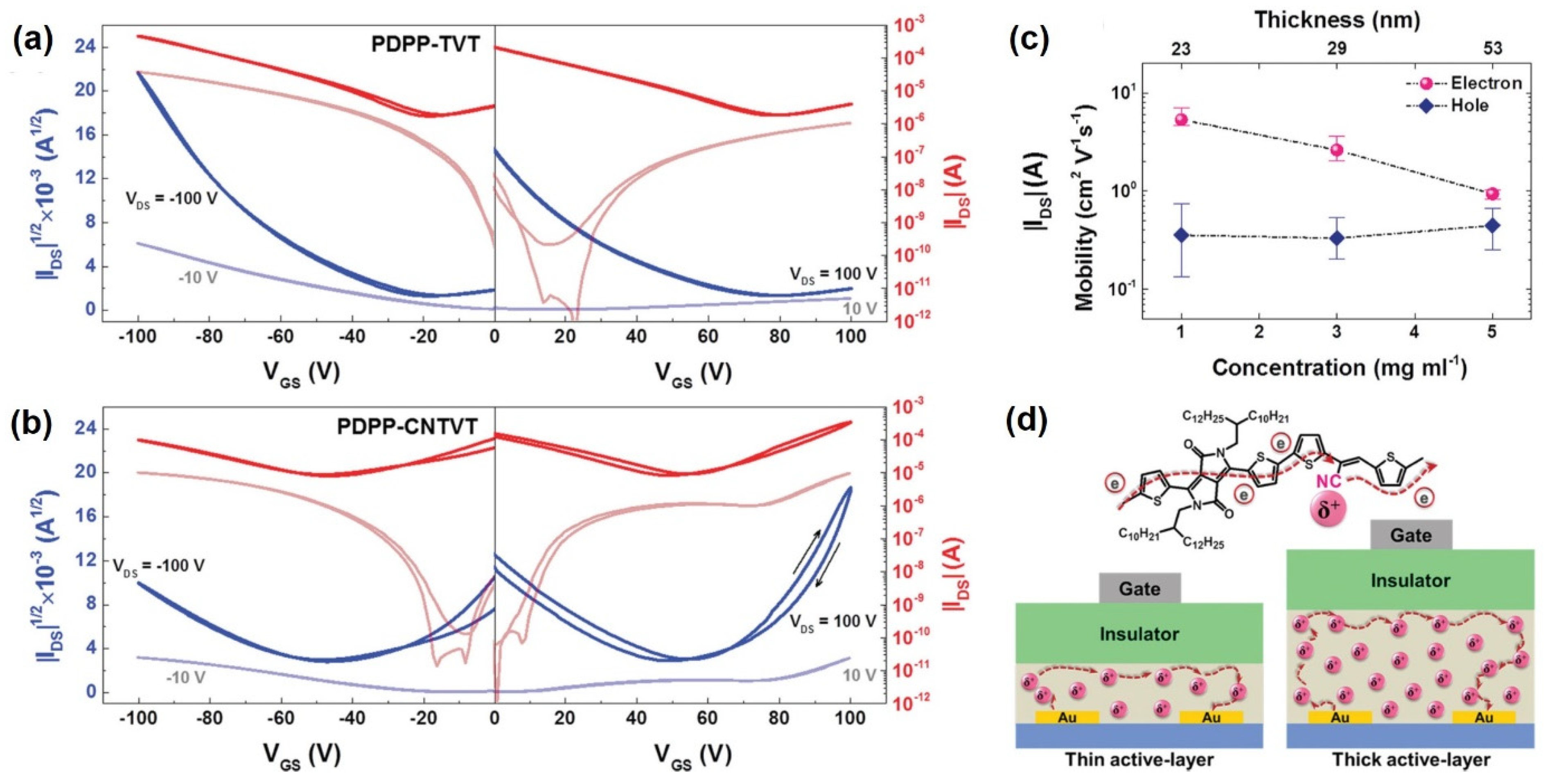
| Yun et al. [81] | PDPP-CNTVT | Ambipolar | Inclusion of a nitrile group in the polymer vinyl linkage results in ambipolar behavior; charge transport depends on active layer thickness | Electron mobility of 7 cm2/Vs |
| Author | Semiconductor | Type | Result Findings | Mobility |
|---|---|---|---|---|
| Kanimozhi et al. [151] | N-CS2DPP-OD-TEG | Ambipolar | Device configuration impacts ambipolar behaviors and charge transport | 3 cm2/Vs (electron) |
| Bronstein et al. [152] | Diketopyrrolopyrrole based polymer | Ambipolar | A much higher hole mobility was obtained than electron mobility | 1.95 cm2/Vs (hole) |
| Wang et al. [153] | PDPPHD-T3 | Ambipolar | Device performance of PDPPHD-T3 thin-film transistor for detecting xylene | 0.125 cm2/Vs (hole) and 0.027 cm2/Vs (electron) |
| Li et al. [78] | PDQT | p-type | High-molecular-weight PDQT exhibits more superior morphology and charge transport | 0.97 cm2/Vs from the high-molecular-weight PDQT |
Disclaimer/Publisher’s Note: The statements, opinions and data contained in all publications are solely those of the individual author(s) and contributor(s) and not of MDPI and/or the editor(s). MDPI and/or the editor(s) disclaim responsibility for any injury to people or property resulting from any ideas, methods, instructions or products referred to in the content. |
© 2024 by the authors. Licensee MDPI, Basel, Switzerland. This article is an open access article distributed under the terms and conditions of the Creative Commons Attribution (CC BY) license (https://creativecommons.org/licenses/by/4.0/).
Share and Cite
He, Z.; Asare-Yeboah, K.; Bi, S. Advances in Charge Carrier Mobility of Diketopyrrolopyrrole-Based Organic Semiconductors. Coatings 2024, 14, 1080. https://doi.org/10.3390/coatings14091080
He Z, Asare-Yeboah K, Bi S. Advances in Charge Carrier Mobility of Diketopyrrolopyrrole-Based Organic Semiconductors. Coatings. 2024; 14(9):1080. https://doi.org/10.3390/coatings14091080
Chicago/Turabian StyleHe, Zhengran, Kyeiwaa Asare-Yeboah, and Sheng Bi. 2024. "Advances in Charge Carrier Mobility of Diketopyrrolopyrrole-Based Organic Semiconductors" Coatings 14, no. 9: 1080. https://doi.org/10.3390/coatings14091080
APA StyleHe, Z., Asare-Yeboah, K., & Bi, S. (2024). Advances in Charge Carrier Mobility of Diketopyrrolopyrrole-Based Organic Semiconductors. Coatings, 14(9), 1080. https://doi.org/10.3390/coatings14091080