
A Review of CIGS Thin Film Semiconductor Deposition via Sputtering and Thermal Evaporation for Solar Cell Applications


Abstract
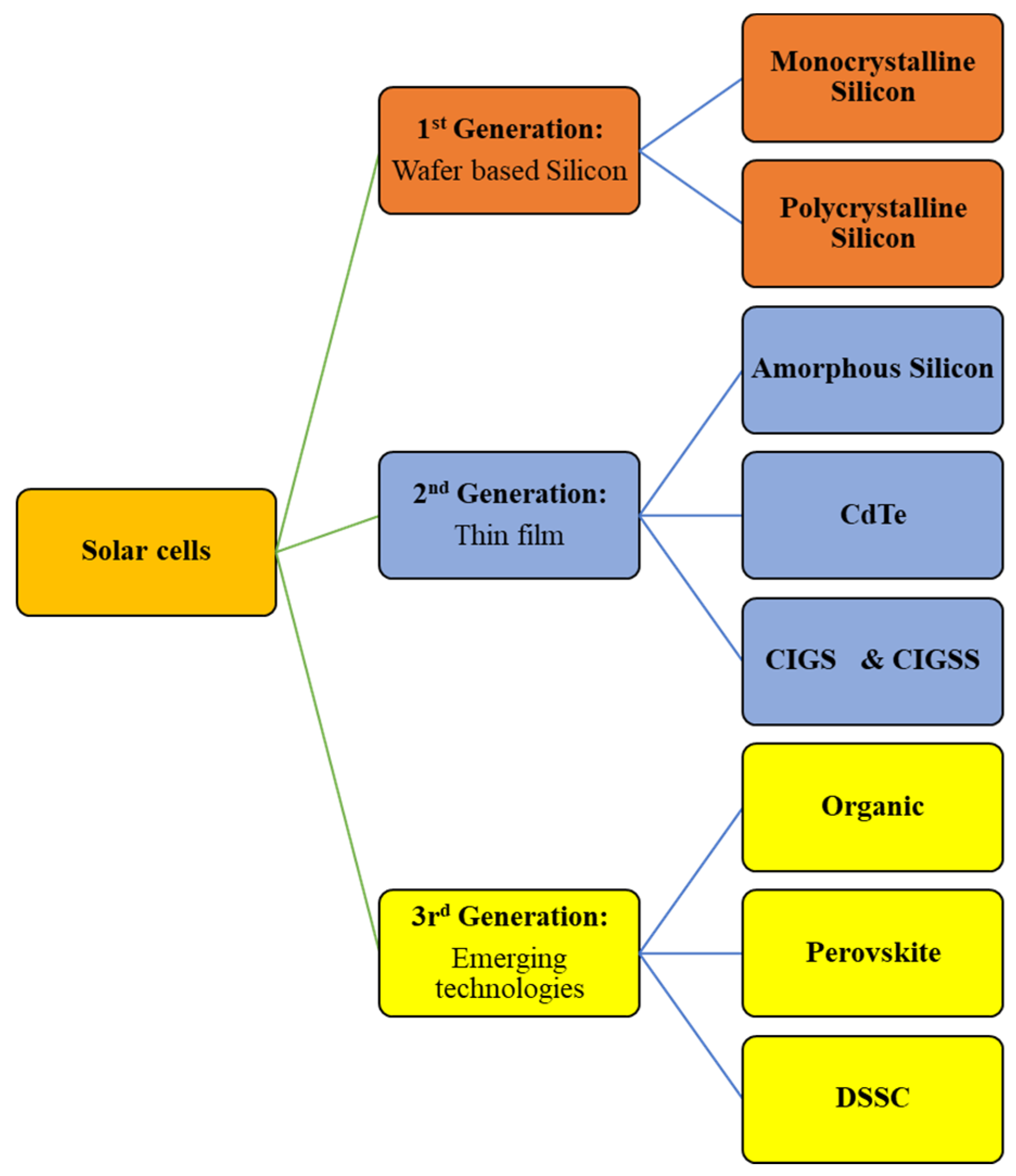
:1. Introduction
- Amorphous Silicon (a-Si): Characterized by disorderedly organized silicon atoms, amorphous silicon differs from crystalline silicon. a-Si solar cells are more cost-effective than their crystalline counterparts due to the reduced silicon requirement. However, the fundamental limitation of this technology lies in its lower efficiency, attributed to material defects [11,12,13].
- Cadmium Telluride (CdTe): Stands out as a direct bandgap material with a higher absorption coefficient and greater chemical stability compared to a-Si. However, the main drawback of CdTe solar cells is the inclusion of cadmium (Cd), a heavy and hazardous metal [11].
- Copper Indium Gallium Di-Selenide (CIGS): A quaternary compound with a direct bandgap and a high absorption coefficient [11].
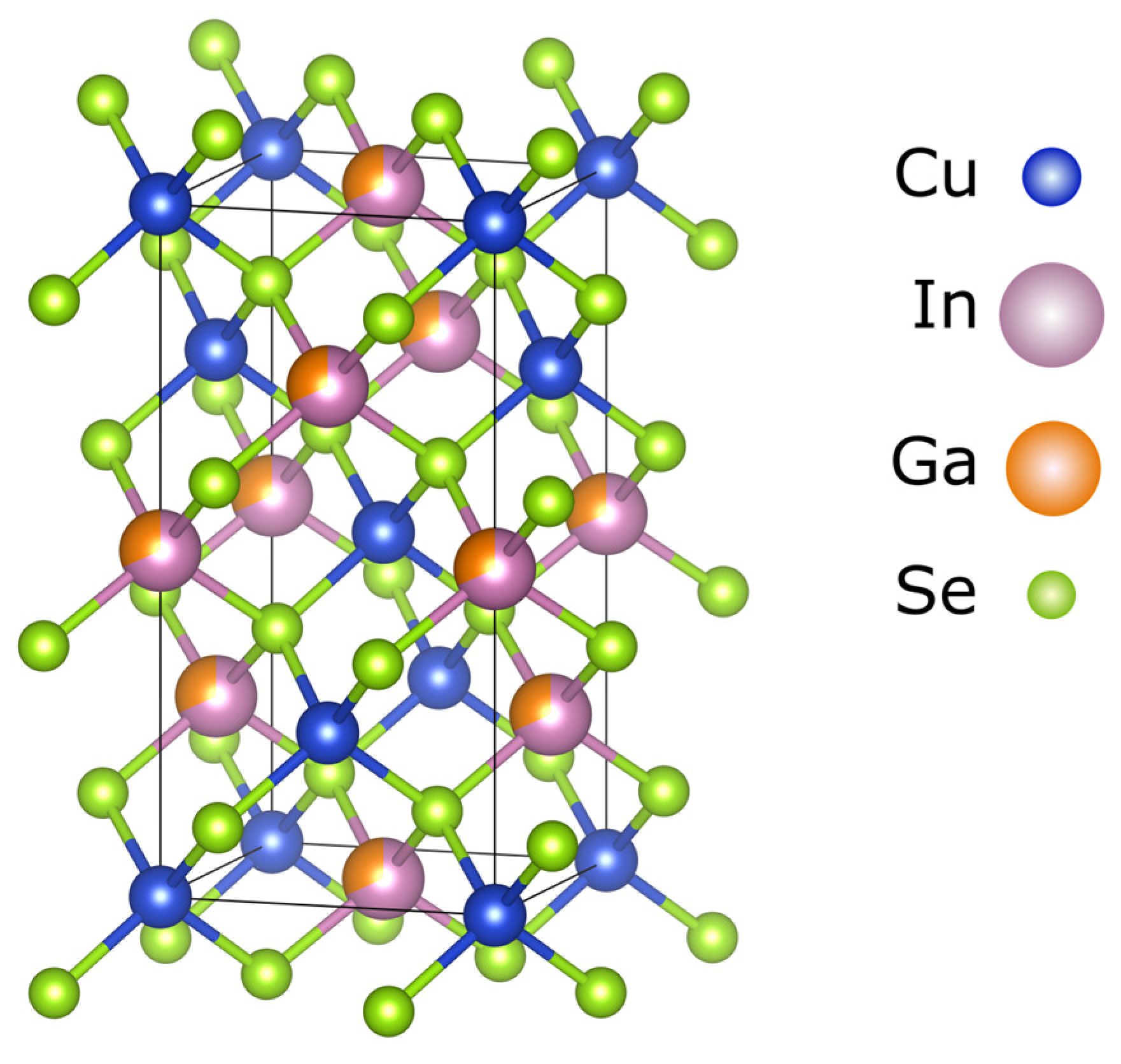
2. Properties of Chalcogenide Materials
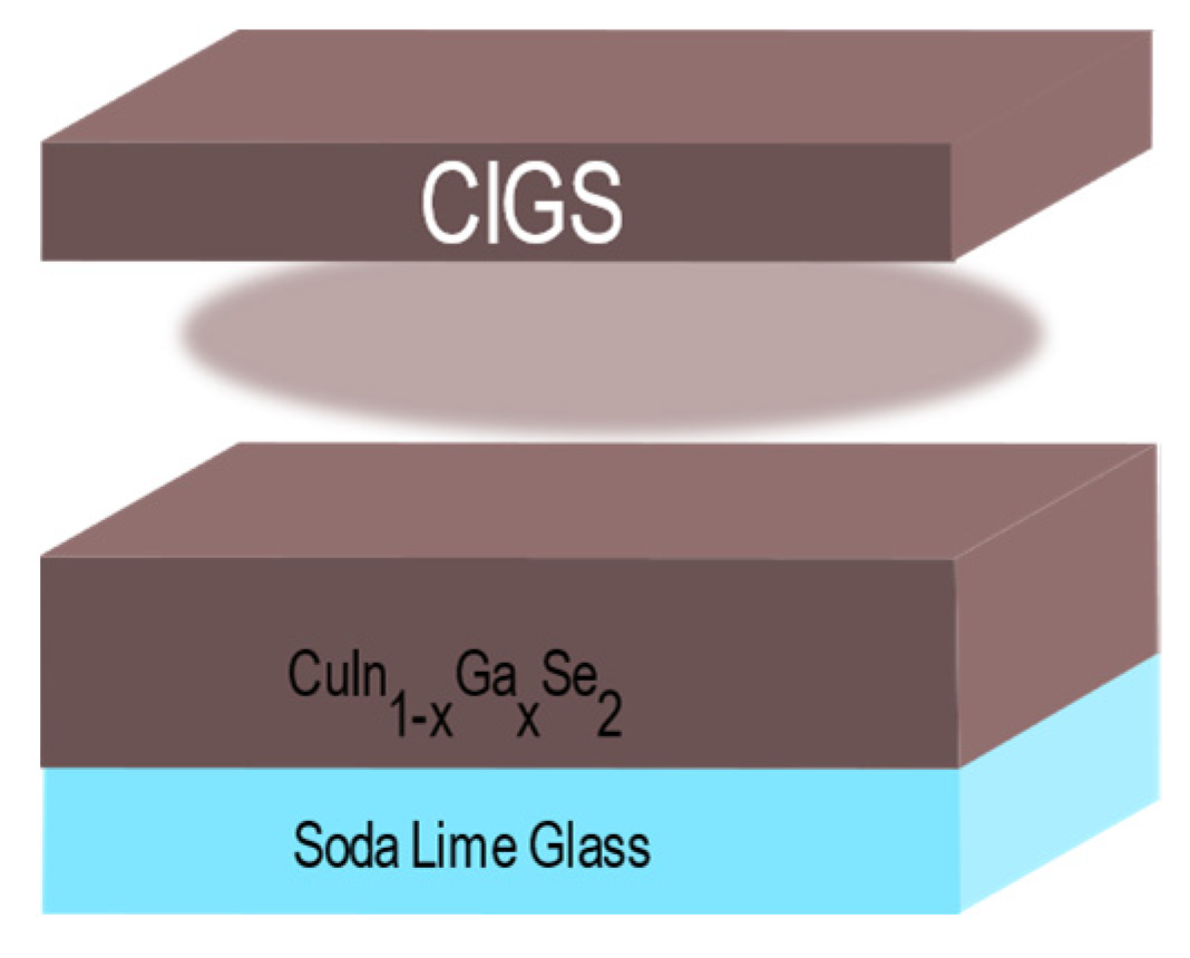
3. Device Architecture of CIGS Solar Cells
4. Challenges with the Deposition of CIGS Thin Films Using Solution-Based Processes
5. Physical Vapor Deposition Methods Used for the Preparation of CIGS Thin Films
5.1. Working Principle of the Deposition Techniques
- Resistive Heating: This method employs a resistively heated source to evaporate the targeted material. The source is typically constructed from refractory metals such as tungsten, molybdenum, and tantalum, which possess high melting points.
- Electron Beam Evaporation: In this technique, a material is evaporated by focusing an intense electron beam on it. Electron beam evaporation addresses challenges associated with resistive heating, including contamination and the difficulty of evaporating materials with high melting points.
- An ion, often an argon ion (Ar), accelerates toward a negatively charged target.
- The accelerated ion hits the target material, leading to a series of atomic collisions.
- As a consequence of these collisions, one or more atoms from the target are ejected and become free in the form of ions or neutral particles.
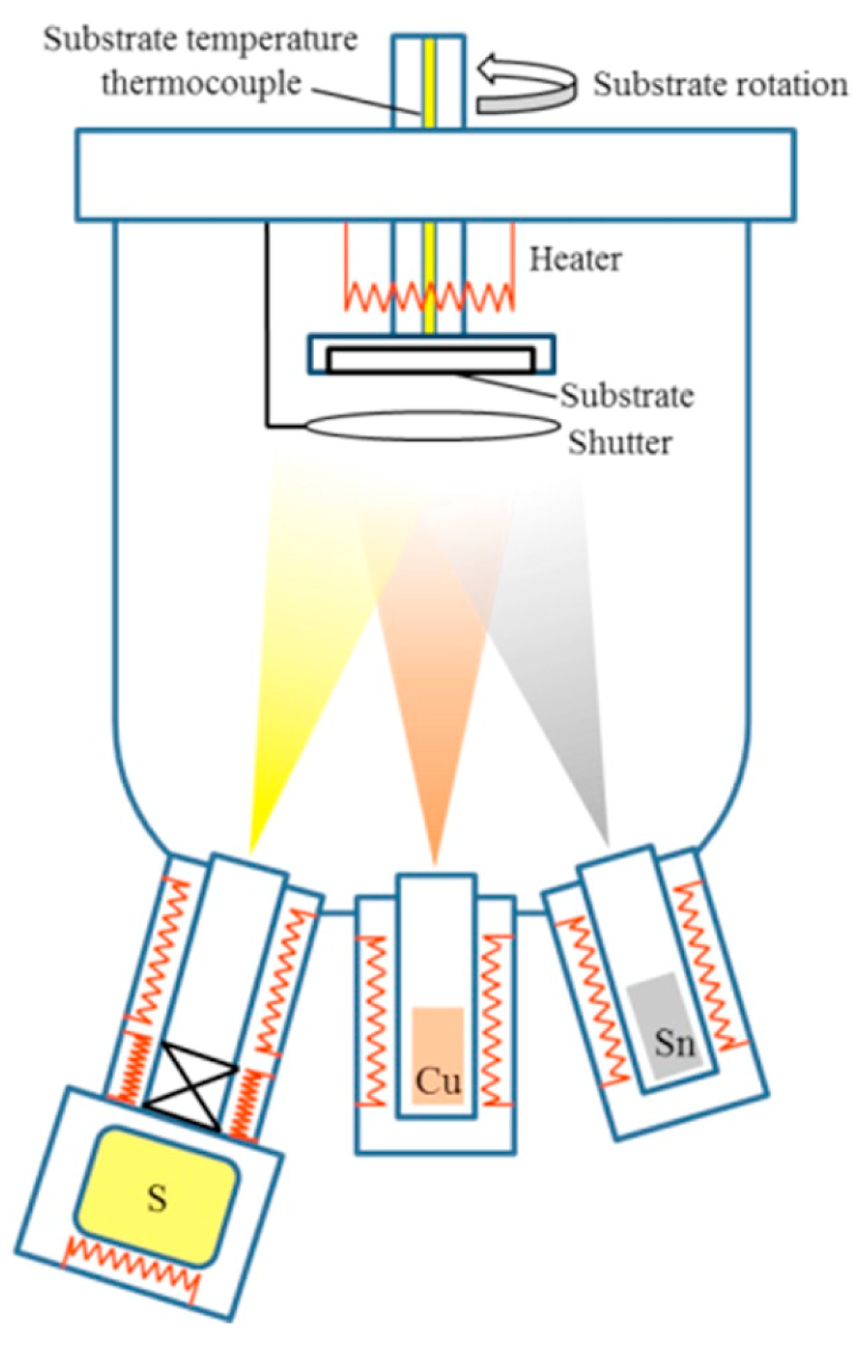
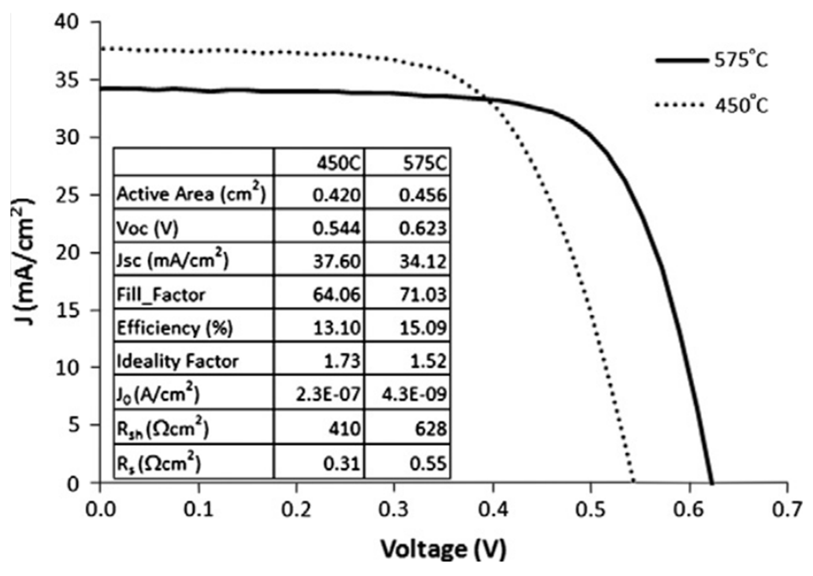
5.2. Deposition of CIGS Films by Thermal Co-Evaporation
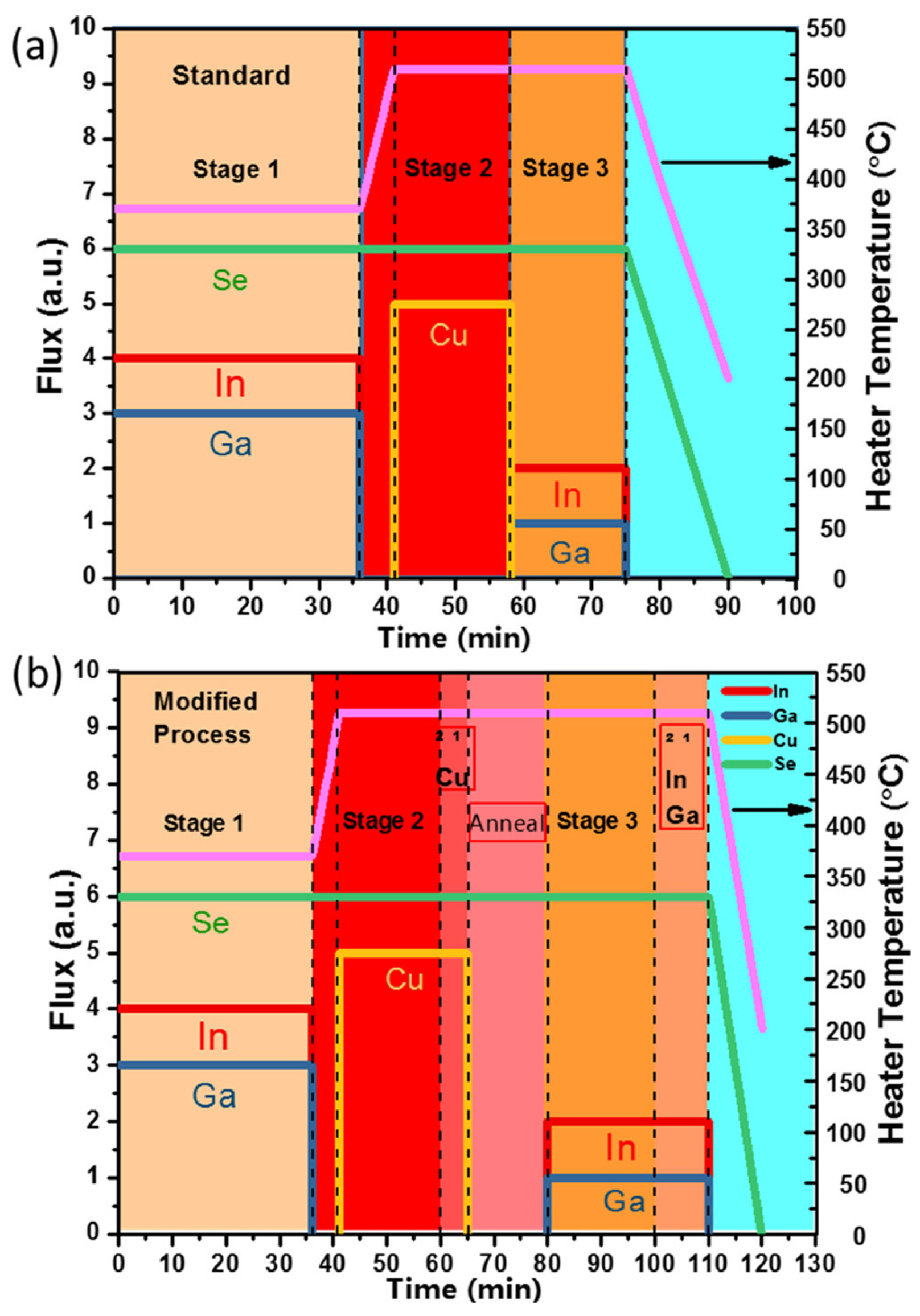
5.2.1. Three-Stage Deposition
5.2.2. Two-Stage Deposition
5.2.3. Single-Stage Deposition
5.3. Deposition of CIGS Films by Sputtering Methods
5.3.1. Two-Step Deposition
5.3.2. Single-Step Deposition

| Device Structure | Deposition of CIGS | PCE (%) | FF (%) | Voc (mV) | Jsc (mA/cm2) | Device Area (cm2) | Ref. |
|---|---|---|---|---|---|---|---|
| MgF2/ZnO/CdS/CIGS/Mo | 20.8 | 79.1 | 757 | 34.8 | 0.5 | [33] | |
| ZnO/CdS/CIGS/Mo | Pulse current electrodeposition | 11.04 | 63.40 | 505 | 34.47 | 0.34 | [56] |
| MgF2/ZnO/CdS/CIGS/Mo | 15.9 | 76.6 | 649 | 31.88 | 0.437 | [72] | |
| MgF2/ZnO/CdS/Cu(In,Ga)Se2/Mo | Three-stage | 18.8 | 78.6 | 678 | 35.2 | [73] | |
| MgF2/ZnO/CdS/Cu (In,Ga)Se2/CuGaSe2/Mo | Two-stage | 17.7 | 77.2 | 674 | 34.0 | 0.414 | [74] |
| MgF2/ZnO/CdS/Cu(In,Ga)Se2/Mo | 19.9 | 81.2 | 690 | 35.5 | 0.419 | [75] | |
| ZnO/CdS/CIGS/Mo | 17.6 | 0.79 | 671 | 33.20 | [76] | ||
| ITO/ZnO/CdS/CIGS/Mo/PI | 13.6 | 67.23 | 620 | 32.75 | 0.5 | [78] | |
| ZnO/CdS/CIGS/Mo | 16.9 | 74.3 | 658 | 34.6 | 0.5 | [79] | |
| MgF2/ZnO/CdS/CIGS/Mo | Multi-stage | 21.7 | 79.3 | 746 | 36.6 | [81] | |
| MgF2/ZnO/CdS/CIGS/Mo | 22.6 | 80.6 | 741 | 37.8 | 0.5 | [82] | |
| ZnO/CdS/CIGS/Mo | 10.14 | 63.0 | 505 | 32.3 | 0.4 | [98] | |
| MgF2/ZnO/CdS/CIGS/Mo | One-step | 16.7 | 70.6 | 614 | 38.6 | 0.86 | [100] |
| ZnO/CdS/CIGS/Mo | Two-step | 13.5 | 70 | 530 | 36.5 | 0.86 | [102] |
| ZnO/CdS/CIGS/Mo | 10.2 | 67.0 | 533 | 28.0 | 0.43 | [104] | |
| 11.2 | 67.9 | 520 | 31.0 | 0.43 | |||
| 13.1 | 69.9 | 563 | 33.0 |
6. Current Status, Challenges, and Future Prospects
- -
- Various types of substrates have been employed for CIGS solar cells, each offering distinct advantages. Soda–lime glass (SLG) stands out as the most commonly used substrate due to its alkali diffusion properties and suitability for relatively high-temperature CIGS solar cell production [110]. Flexible substrates have also gained attention, offering the advantage of the low-temperature deposition of CIGS thin films. Polyimide substrates, for example, have achieved an efficiency of 18.7% [111]. In cases where high-temperature processing is required, ceramics can serve as flexible substrates, providing an alternative to rigid SLG [110].
- -
- The Mo thin film has demonstrated its effectiveness as a suitable back contact for CIGS solar cells. However, the challenge lies in simultaneously achieving both good adhesion and low resistivity in this material [111]. To address this, a bilayer approach is often employed instead of a single layer. The first layer is designed for high adhesion, while the second layer serves as a low-resistivity thin film [112]. The selenization process, leading to the formation of a MoSe2 layer, has been found to enhance the adhesion of the CIGS thin film on Mo, preventing interface recombination [113]. The thickness of the MoSe2 layer is a crucial factor influencing its impact on the Mo/CIGS interface properties [50], although controlling its thickness during the selenization step can be challenging [110]. To address this, an alternative approach is to deposit all cell layers using sputtering with an interlayer of MoSe2, providing greater control over the process.
- -
- The most commonly used buffer layer for CIGS solar cells is CdS. However, CdS has a relatively low band gap of about 2.4 eV, which can result in the absorption of light, particularly in short wavelengths [114]. To address this issue and replace the toxic cadmium with more environmentally friendly elements, various alternatives have been explored. These alternatives include ZnO [115], ZnSe [116], Zn(O,S) [117], ZnMgO [118], ZnSnO [119], and In2S3 [120].
- -
- Indium scarcity and high demand might contribute to an increase in the cost of CIGS solar cells. CZTS-based solar cells were developed to substitute Zn for In; however, their power conversion efficiencies are still very low to compete with CIGS counterparts. The substitution of more In for Ga is another way to reduce In usage, which also comes with the advantage of a larger band gap, allowing its use as a top cell in tandem devices. An alternative approach consists of reducing the thickness of the absorber layer so that it is lower than 400 nm [121]. Recent numerical models predict the possibility of reaching efficiencies as high as 21% for these ultra-thin solar cells [122]. This would reduce the material use and increase the production throughput.
- -
- The “tandem solar cell” approach involves combining two or more junctions in a solar cell. In this configuration, the top junction is designed to absorb high-energy photons, while the bottom junction is responsible for absorbing low-energy photons [123]. One promising tandem solar cell configuration is the perovskite/CIGS tandem solar cell, which has demonstrated an efficiency exceeding 24% according to the National Renewable Energy Laboratory (NREL). This tandem configuration leverages the strengths of both perovskite and CIGS materials to enhance overall solar cell performance.
7. Conclusions
Author Contributions
Funding
Institutional Review Board Statement
Informed Consent Statement
Data Availability Statement
Conflicts of Interest
References
- Al-Mulali, U.; Fereidouni, H.G.; Lee, J.Y.M. Electricity Consumption from Renewable and Non-Renewable Sources and Economic Growth: Evidence from Latin American Countries. Renew. Sustain. Energy Rev. 2014, 30, 290–298. [Google Scholar] [CrossRef]
- Zahedi, A. A Review of Drivers, Benefits, and Challenges in Integrating Renewable Energy Sources into Electricity Grid. Renew. Sustain. Energy Rev. 2011, 15, 4775–4779. [Google Scholar] [CrossRef]
- Moheimani, N.R.; Parlevliet, D. Sustainable Solar Energy Conversion to Chemical and Electrical Energy. Renew. Sustain. Energy Rev. 2013, 27, 494–504. [Google Scholar] [CrossRef]
- Mohammad Bagher, A. Types of Solar Cells and Application. Am. J. Opt. Photonics 2015, 3, 94. [Google Scholar] [CrossRef]
- Sundaram, S.; Benson, D.; Mallick, T.K. Overview of the PV Industry and Different Technologies. In Solar Photovoltaic Technology Production; Academic Press: Cambridge, MA, USA, 2016; ISBN 978-0-12-802953-4. [Google Scholar] [CrossRef]
- Lee, T.D.; Ebong, A.U. A Review of Thin Film Solar Cell Technologies and Challenges. Renew. Sustain. Energy Rev. 2017, 70, 1286–1297. [Google Scholar] [CrossRef]
- Okil, M.; Salem, M.S.; Abdolkader, T.M.; Shaker, A. From Crystalline to Low-Cost Silicon-Based Solar Cells: A Review. Silicon 2022, 14, 1895–1911. [Google Scholar] [CrossRef]
- Shah, A.V.; Platz, R.; Keppner, H. Thin-Film Silicon Solar Cells: A Review and Selected Trends. Sol. Energy Mater. Sol. Cells 1995, 38, 501–520. [Google Scholar] [CrossRef]
- Prasad, R.D.; Bansal, R.C. Photovoltaic Systems. In Handbook of Renewable Energy Technology; World Scientific: Singapore, 2011; pp. 205–224. [Google Scholar] [CrossRef]
- Ramanujam, J.; Singh, U.P. Copper Indium Gallium Selenide Based Solar Cells—A Review. Energy Environ. Sci. 2017, 10, 1306–1319. [Google Scholar] [CrossRef]
- Sharma, S.; Jain, K.K.; Sharma, A. Solar Cells: In Research and Applications—A Review. Mater. Sci. Appl. 2015, 06, 1145–1155. [Google Scholar] [CrossRef]
- Stuckelberger, M.; Biron, R.; Wyrsch, N.; Haug, F.J.; Ballif, C. Review: Progress in Solar Cells from Hydrogenated Amorphous Silicon. Renew. Sustain. Energy Rev. 2017, 76, 1497–1523. [Google Scholar] [CrossRef]
- Sreejith, S.; Ajayan, J.; Kollem, S.; Sivasankari, B. A Comprehensive Review on Thin Film Amorphous Silicon Solar Cells. Silicon 2022, 14, 8277–8293. [Google Scholar] [CrossRef]
- Sahu, A.; Garg, A.; Dixit, A. A Review on Quantum Dot Sensitized Solar Cells: Past, Present and Future towards Carrier Multiplication with a Possibility for Higher Efficiency. Sol. Energy 2020, 203, 210–239. [Google Scholar] [CrossRef]
- Krebs, F.C. Fabrication and Processing of Polymer Solar Cells: A Review of Printing and Coating Techniques. Sol. Energy Mater. Sol. Cells 2009, 93, 394–412. [Google Scholar] [CrossRef]
- Sugathan, V.; John, E.; Sudhakar, K. Recent Improvements in Dye Sensitized Solar Cells: A Review. Renew. Sustain. Energy Rev. 2015, 52, 54–64. [Google Scholar] [CrossRef]
- Hasan, A.; Sarwar, J.; Shah, A.H. Concentrated Photovoltaic: A Review of Thermal Aspects, Challenges and Opportunities. Renew. Sustain. Energy Rev. 2018, 94, 835–852. [Google Scholar] [CrossRef]
- Gulkowski, S.; Zdyb, A.; Dragan, P. Experimental Efficiency Analysis of a Photovoltaic System with Different Module Technologies under Temperate Climate Conditions. Appl. Sci. 2019, 9, 141. [Google Scholar] [CrossRef]
- Ghanbari, E.; Zahedifar, M.; Moradi, M. Improving CIGS Thin Film by Evaporation of CIGS Nanoparticles without Phase Change. Appl. Phys. A Mater. Sci. Process. 2019, 125, 327. [Google Scholar] [CrossRef]
- Suresh, S.; Uhl, A.R. Present Status of Solution-Processing Routes for Cu(In,Ga)(S,Se)2 Solar Cell Absorbers. Adv. Energy Mater. 2021, 11, 2003743. [Google Scholar] [CrossRef]
- Gonçalves, B.F.; Sadewasser, S.; Salonen, L.M.; Lanceros-Méndez, S.; Kolen’ko, Y.V. Merging Solution Processing and Printing for Sustainable Fabrication of Cu(In,Ga)Se2 Photovoltaics. Chem. Eng. J. 2022, 442, 136188. [Google Scholar] [CrossRef]
- Kazmerski, L.L.; White, F.R.; Morgan, G.K. Thin-Film CuInSe2/CdS Heterojunction Solar Cells. Appl. Phys. Lett. 1976, 29, 268–270. [Google Scholar] [CrossRef]
- Kazmerski, L.L.; White, F.R.; Ayyagari, M.S.; Juang, Y.J.; Patterson, R.P. Growth and Characterization of Thin-film Compound Semiconductor Photovoltaic Heterojunctions. J. Vac. Sci. Technol. 1976, 14, 65–68. [Google Scholar] [CrossRef]
- Abou-Ras, D.; Kostorz, G.; Romeo, A.; Rudmann, D.; Tiwari, A.N. Structural and Chemical Investigations of CBD- and PVD-CdS Buffer Layers and Interfaces in Cu(In,Ga)Se2-Based Thin Film Solar Cells. Thin Solid Film. 2005, 480–481, 118–123. [Google Scholar] [CrossRef]
- Gloeckler, M.; Sites, J.R. Efficiency Limitations for Wide-Band-Gap Chalcopyrite Solar Cells. Thin Solid Film. 2005, 480–481, 241–245. [Google Scholar] [CrossRef]
- Luque, A.; Hegedus, S. Handbook of Photovoltaic Science and Engineering; John Wiley & Sons, Ltd.: Hoboken, NJ, USA, 2011; ISBN 9780470721698. [Google Scholar]
- Momma, K.; Izumi, F. VESTA 3 for Three-Dimensional Visualization of Crystal, Volumetric and Morphology Data. J. Appl. Crystallogr. 2011, 44, 1272–1276. [Google Scholar] [CrossRef]
- Faraj, M.G.; Ibrahim, K.; Salhin, A. Effects of Ga Concentration on Structural and Electrical Properties of Screen Printed-CIGS Absorber Layers on Polyethylene Terephthalate. Mater. Sci. Semicond. Process. 2012, 15, 206–213. [Google Scholar] [CrossRef]
- Jung, S.; Ahn, S.J.; Yun, J.H.; Gwak, J.; Kim, D.; Yoon, K. Effects of Ga Contents on Properties of CIGS Thin Films and Solar Cells Fabricated by Co-Evaporation Technique. Curr. Appl. Phys. 2010, 10, 990–996. [Google Scholar] [CrossRef]
- Yoshiaki, H.; Yasuyoshi, K.; Akira, Y. Numerical Study of Cu(In,Ga)Se 2 Solar Cell Performance toward 23% Conversion Efficiency. Jpn. J. Appl. Phys. 2014, 53, 12301. [Google Scholar] [CrossRef]
- Mudryi, A.V.; Gremenok, V.F.; Karotki, A.V.; Zalesski, V.B.; Yakushev, M.V.; Luckert, F.; Martin, R. Structural and Optical Properties of Thin Films of Cu(In,Ga)Se2 Semiconductor Compounds. J. Appl. Spectrosc. 2010, 77, 371–377. [Google Scholar] [CrossRef]
- Mufti, N.; Amrillah, T.; Taufiq, A.; Diantoro, M.; Nur, H. Review of CIGS-Based Solar Cells Manufacturing by Structural Engineering. Sol. Energy 2020, 207, 1146–1157. [Google Scholar] [CrossRef]
- Jackson, P.; Hariskos, D.; Lotter, E.; Paetel, S.; Wuerz, R.; Menner, R.; Wischmann, W.; Powalla, M. New World Record Efficiency for Cu(In,Ga)Se2 Thin-Film Solar Cells beyond 20%. Prog. Photovolt. Res. Appl. 2011, 19, 894–897. [Google Scholar] [CrossRef]
- Diagne, O.; Ehemba, A.K.; Diallo, D.; Wade, I.; Soce, M.; Dieng, M. Effect of [Ga]/[In + Ga] Atomic Ratio on Electric Parameters of Cu(In,Ga)Se2 Thin Film Solar Cells. Int. J. Sci. Eng. Technol. 2016, 5, 252–255. [Google Scholar] [CrossRef]
- Jo, H.J.; Kim, D.H.; Kim, C.; Hwang, D.K.; Sung, S.J.; Kim, J.H.; Bae, I.H. The Optical and Structural Properties of CuIn 1-XGa XSe 2 Thin Films Fabricated with Various Ga Contents by Using the Co-Evaporation Technique. J. Korean Phys. Soc. 2012, 60, 1708–1712. [Google Scholar] [CrossRef]
- Li, H.; Qu, F.; Luo, H.; Niu, X.; Chen, J.; Zhang, Y.; Yao, H.; Jia, X.; Gu, H.; Wang, W. Engineering CIGS Grains Qualities to Achieve High Efficiency in Ultrathin Cu(InxGa1−x)Se2 Solar Cells with a Single-Gradient Band Gap Profile. Results Phys. 2019, 12, 704–711. [Google Scholar] [CrossRef]
- Jasenek, A.; Rau, U.; Nadenau, V.; Schock, H.W. Electronic Properties of CuGaSe2-Based Heterojunction Solar Cells. Part II. Defect Spectroscopy. J. Appl. Phys. 2000, 87, 594–602. [Google Scholar] [CrossRef]
- Wei, S.H.; Zhang, S.B.; Zunger, A. Effects of Ga Addition to CuInSe2 on Its Electronic, Structural, and Defect Properties. Appl. Phys. Lett. 1998, 72, 3199–3201. [Google Scholar] [CrossRef]
- Huang, C.H. Effects of Ga Content on Cu(In,Ga)Se2 Solar Cells Studied by Numerical Modeling. J. Phys. Chem. Solids 2008, 69, 330–334. [Google Scholar] [CrossRef]
- Zhang, Z.; Witte, W.; Kiowski, O.; Lemmer, U.; Powalla, M.; Hölscher, H. Influence of the Ga Content on the Optical and Electrical Properties of CuIn 1-XGa XSe2 Thin-Film Solar Cells. IEEE J. Photovolt. 2013, 3, 823–827. [Google Scholar] [CrossRef]
- Guthrey, H.; Contreras, M.; Al-Jassim, M. The Effect of Ga Content on the Recombination Behavior of Grain Boundaries in Cu(In,Ga)Se2 Solar Cells. MRS Online Proc. Libr. 2014, 1670, mrss14-1670. [Google Scholar] [CrossRef]
- Bai, T.R.; Liu, C.Q.; Wang, N.; Liu, S.M.; Wang, H.L.; Jiang, W.W.; Ding, W.Y.; Fei, W.D.; Chai, W.P. Effects of Sputtering Voltage and Current on the Composition and Microstructure of the CIGS Films Prepared by One-Step Pulsed DC Magnetron Sputtering. J. Alloys Compd. 2015, 646, 532–540. [Google Scholar] [CrossRef]
- Rahman, M.F.; Hossain, J.; Kuddus, A.; Tabassum, S.; Rubel, M.H.K.; Shirai, H.; Ismail, A.B.M. A Novel Synthesis and Characterization of Transparent CdS Thin Films for CdTe/CdS Solar Cells. Appl. Phys. A Mater. Sci. Process. 2020, 126, 1–11. [Google Scholar] [CrossRef]
- Ayachi, B.; Aviles, T.; Vilcot, J.P.; Sion, C.; Miska, P. Room Temperature Pulsed-DC Sputtering Deposition Process for CIGS Absorber Layer: Material and Device Characterizations. Thin Solid Film. 2018, 660, 175–179. [Google Scholar] [CrossRef]
- Suryavanshi, P.S.; Panchal, C.J.; Patel, A.L. Influence of Thickness on Physical and Optoelectronic Properties of DC Sputtered Bilayer Molybdenum Thin Films for CIGS Solar Cell. Mater. Today Proc. 2019, 39, 1884–1888. [Google Scholar] [CrossRef]
- Li, W.; Zhao, Y.M.; Liu, X.J.; Ao, J.P.; Sun, Y. Thickness Optimization of Mo Films for Cu(InGa)Se2 Solar Cell Applications. Chin. Phys. B 2011, 20, 068102. [Google Scholar] [CrossRef]
- Chia-Hao, H.; Yue-Shun, S.; Shih-Yuan, W.; Chia-Hsiang, C.; Wei-Hao, H.; Chang, C.; Yan-Huie, W.; Chun-Jun, L.; Chih-Huang, L. Na-induced Efficiency Boost for Se-deficient Cu In Ga Se2 Solar Cells. Prog. Photovolt. Res. Appl. 2015, 23, 1621. [Google Scholar] [CrossRef]
- Orgassa, K.; Schock, H.W.; Werner, J.H. Alternative Back Contact Materials for Thin Film Cu(In,Ga)Se2 Solar Cells. Thin Solid Film. 2003, 431–432, 387–391. [Google Scholar] [CrossRef]
- Cao, Q.; Gunawan, O.; Copel, M.; Reuter, K.B.; Chey, S.J.; Deline, V.R.; Mitzi, D.B. Defects in Cu(In,Ga)Se 2 Chalcopyrite Semiconductors: A Comparative Study of Material Properties, Defect States, and Photovoltaic Performance. Adv. Energy Mater. 2011, 1, 845–853. [Google Scholar] [CrossRef]
- Hsiao, K.J.; Liu, J.D.; Hsieh, H.H.; Jiang, T.S. Electrical Impact of MoSe2 on CIGS Thin-Film Solar Cells. Phys. Chem. Chem. Phys. 2013, 15, 18174–18178. [Google Scholar] [CrossRef] [PubMed]
- Dai, W.; Gao, Z.; Li, J.; Qin, S.; Wang, R.; Xu, H.; Wang, X.; Gao, C.; Teng, X.; Zhang, Y.; et al. Above 15% Efficient Directly Sputtered CIGS Solar Cells Enabled by a Modified Back-Contact Interface. ACS Appl. Mater. Interfaces 2021, 13, 49414–49422. [Google Scholar] [CrossRef] [PubMed]
- Wada, T.; Kohara, N.; Nishiwaki, S.; Negami, T. Characterization of the Cu(In,Ga)Se2/Mo Interface in CIGS Solar Cells. Thin Solid Film. 2001, 387, 118–122. [Google Scholar] [CrossRef]
- Cheng, K.; Liu, J.; Jin, R.; Liu, J.; Liu, X.; Lu, Z.; Liu, Y.; Liu, X.; Du, Z. Surface Microstructure Evolution of Highly Transparent and Conductive Al-Doped ZnO Thin Films and Its Application in CIGS Solar Cells. Appl. Surf. Sci. 2017, 409, 124–131. [Google Scholar] [CrossRef]
- Kaelin, M.; Rudmann, D.; Tiwari, A.N. Low Cost Processing of CIGS Thin Film Solar Cells. Sol. Energy 2004, 77, 749–756. [Google Scholar] [CrossRef]
- Bi, J.; Gao, Q.; Ao, J.; Zhang, Z.; Sun, G.; Zhang, Y.; Liu, W.; Liu, F.; Sun, Y.; Xiang, D. Influence of Cu on Ga Diffusion during Post-Selenizing the Electrodeposited Cu/In/Ga Metallic Precursor Process. Sol. Energy Mater. Sol. Cells 2018, 182, 92–97. [Google Scholar] [CrossRef]
- Bi, J.; Ao, J.; Gao, Q.; Zhang, Z.; Sun, G.; He, Q.; Zhou, Z.; Sun, Y.; Zhang, Y. Controllable Growth of Ga Film Electrodeposited from Aqueous Solution and Cu(In,Ga)Se2 Solar Cells. ACS Appl. Mater. Interfaces 2017, 9, 18682–18690. [Google Scholar] [CrossRef]
- Gao, Q.; Cao, C.; Ao, J.; Bi, J.; Yao, L.; Guo, J.; Sun, G.; Liu, W.; Zhang, Y.; Liu, F.; et al. Efficiency Improvement of Electrodeposition-Processed Cu(In,Ga)Se2 Solar Cell with Widen Surface Bandgap by Spin-Coating In2S3 Thin Film. Appl. Surf. Sci. 2022, 578, 152063. [Google Scholar] [CrossRef]
- Gao, Q.; Yuan, S.; Zhou, Z.; Kou, D.; Zhou, W.; Meng, Y.; Qi, Y.; Han, L.; Wu, S. Over 16% Efficient Solution-Processed Cu(In,Ga)Se2 Solar Cells via Incorporation of Copper-Rich Precursor Film. Small 2022, 18, 2203443. [Google Scholar] [CrossRef] [PubMed]
- Zhang, T.; Yang, Y.; Liu, D.; Tse, S.C.; Cao, W.; Feng, Z.; Chen, S.; Qian, L. High Efficiency Solution-Processed Thin-Film Cu(In,Ga)(Se,S)2 Solar Cells. Energy Environ. Sci. 2016, 9, 3674–3681. [Google Scholar] [CrossRef]
- Uhl, A.R.; Katahara, J.K.; Hillhouse, H.W. Molecular-Ink Route to 13.0% Efficient Low-Bandgap CuIn(S,Se)2 and 14.7% Efficient Cu(In,Ga)(S,Se)2 Solar Cells. Energy Environ. Sci. 2016, 9, 130–134. [Google Scholar] [CrossRef]
- Ahn, S.; Kim, C.; Yun, J.H.; Gwak, J.; Jeong, S.; Ryu, B.H.; Yoon, K. CuInSe2 (CIS) Thin Film Solar Cells by Direct Coating and Selenization of Solution Precursors. J. Phys. Chem. C 2010, 114, 8108–8113. [Google Scholar] [CrossRef]
- Messier, R. Thin Film Deposition Processes. MRS Bull. 1988, 13, 18–21. [Google Scholar] [CrossRef]
- Sasagawa, S.; Yago, A.; Kanai, A.; Araki, H. Cu2(Sn1−xGex)S3 Solar Cells Prepared via Co-Evaporation and Annealing in Germanium Sulfide and Sulfur Vapor. Phys. Status Solidi Curr. Top. Solid State Phys. 2017, 14, 2–6. [Google Scholar] [CrossRef]
- Abegunde, O.O.; Akinlabi, E.T.; Oladijo, O.P.; Akinlabi, S.; Ude, A.U. Overview of Thin Film Deposition Techniques. AIMS Mater. Sci. 2019, 6, 174–199. [Google Scholar] [CrossRef]
- Alfonso, E.; Olaya, J.; Cubillos, G. Thin Film Growth Through Sputtering Technique and Its Applications. Cryst.-Sci. Technol. 2012, 23, 11–12. [Google Scholar] [CrossRef]
- Mubarak, A.; Hamzah, E.; Toff, M.R.M. Review of Physical Vapour Deposition (PVD) Techniques for Hard Coating. J. Mek. 2005, 20, 42–51. [Google Scholar] [CrossRef]
- Kelly, P.; Arnell, R. Magnetron Sputtering: A Review of Recent Developments and Applications. Vacuum 2000, 56, 159–172. [Google Scholar] [CrossRef]
- Baptista, A.; Silva, F.; Porteiro, J.; Míguez, J.; Pinto, G. Sputtering Physical Vapour Deposition (PVD) Coatings: A Critical Review on Process Improvement Andmarket Trend Demands. Coatings 2018, 8, 402. [Google Scholar] [CrossRef]
- Anders, A. Deposition Rates of High Power Impulse Magnetron Sputtering: Physics and Economics. J. Vac. Sci. Technol. A Vac. Surf. Film. 2010, 28, 783–790. [Google Scholar] [CrossRef]
- Tiron, V.; Velicu, I.L.; Mihăilă, I.; Popa, G. Deposition Rate Enhancement in HiPIMS through the Control of Magnetic Field and Pulse Configuration. Surf. Coat. Technol. 2018, 337, 484–491. [Google Scholar] [CrossRef]
- Alami, J.; Stranak, V.; Herrendorf, A.P.; Hubicka, Z.; Hippler, R. Design of Magnetic Field Configuration for Controlled Discharge Properties in Highly Ionized Plasma. Plasma Sources Sci. Technol. 2015, 24, 045016. [Google Scholar] [CrossRef]
- Gabor, A.M.; Tuttle, J.R.; Albin, D.S.; Contreras, M.A.; Noufi, R.; Hermann, A.M. High-Efficiency CuInxGa1-XSe2 Solar Cells Made from (Inx,Ga1−x)2Se3 Precursor Films. Appl. Phys. Lett. 1994, 65, 198–200. [Google Scholar] [CrossRef]
- Contreras, M.A.; Egaas, B.; Ramanathan, K.; Hiltner, J.; Swartzlander, A.; Hasoon, F.; Noufi, R. Progress Toward 20% Effciency in Cu(In,Ga)Se2 Polycrystalline Thin-Film Solar Cells. Prog. Photovolt. 1999, 7, 311–316. [Google Scholar] [CrossRef]
- Tuttle, J.R.; Ward, J.S.; Duda, A.; Berens, T.A.; Contreras, M.A.; Ramanathan, K.R.; Tennant, A.L.; Keane, J.; Cole, E.D.; Emery, K.; et al. The Performance of Cu(In,Ga)Se 2-Based Solar Cells in Conventional and Concentrator Applications. In Proceedings of the MRS Online Proceedings Library (OPL); Cambridge University Press: Cambridge, UK, 1996; Volume 426, pp. 143–151. [Google Scholar]
- Repins, I.; Contreras, M.A.; Egaas, B.; DeHart, C.; Scharf, J.; Perkins, C.L.; To, B.; Noufi, R. 19.9%-Efficient ZnO/CdS/CuInGaSe2 Solar Cell with 81.2% Fill Factor. Prog. Photovolt. Res. Appl. 2008, 16, 235–239. [Google Scholar] [CrossRef]
- Chaisitsak, S.; Yamada, A.; Konagai, M. Preferred Orientation Control of Cu(In1−x Gax)Se2 (x ≈ 0.28) Thin Films and Its Influence on Solar Cell Characteristics. Jpn. J. Appl. Phys. Part 1 Regul. Pap. Short Notes Rev. Pap. 2002, 41, 507–513. [Google Scholar] [CrossRef]
- Kim, S.Y.; Yoo, H.; Rana, T.R.; Enkhbat, T.; Han, G.; Kim, J.H.; Song, S.; Kim, K.; Gwak, J.; Eo, Y.J.; et al. Effect of Crystal Orientation and Conduction Band Grading of Absorber on Efficiency of Cu(In,Ga)Se2 Solar Cells Grown on Flexible Polyimide Foil at Low Temperature. Adv. Energy Mater. 2018, 8, 1801501. [Google Scholar] [CrossRef]
- Contreras, M.A.; Romero, M.J.; Noufi, R. Characterization of Cu(In,Ga)Se2 Materials Used in Record Performance Solar Cells. Thin Solid Film. 2006, 511–512, 51–54. [Google Scholar] [CrossRef]
- Li, W.; Yao, L.; Li, K.; Li, X.; Yang, B.; Xu, S.; Shi, S.; Yi, C.; Chen, M.; Feng, Y.; et al. Enabling Low-Temperature Deposition of High-Efficiency CIGS Solar Cells with a Modified Three-Stage Co-Evaporation Process. ACS Appl. Energy Mater. 2020, 3, 4201–4207. [Google Scholar] [CrossRef]
- Chirilǎ, A.; Seyrling, S.; Buecheler, S.; Guettler, D.; Nishiwaki, S.; Romanyuk, Y.E.; Bilger, G.; Tiwari, A.N. Influence of High Growth Rates on Evaporated Cu(In,Ga)Se 2 Layers and Solar Cells. Prog. Photovolt. Res. Appl. 2012, 20, 209–216. [Google Scholar] [CrossRef]
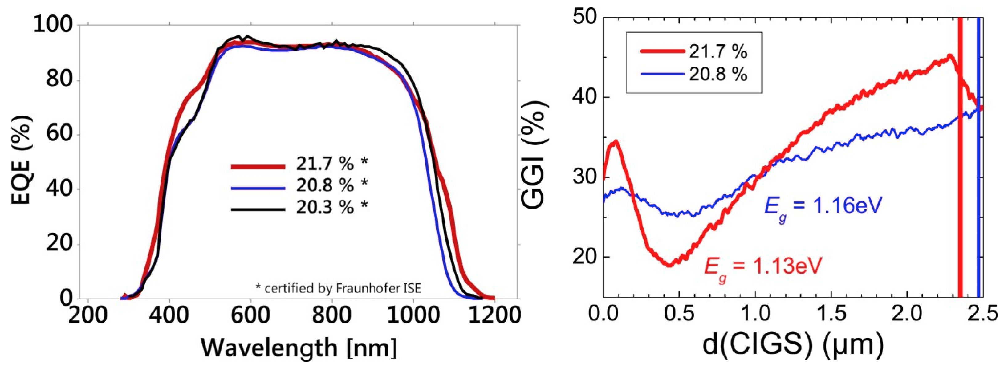
- Jackson, P.; Hariskos, D.; Wuerz, R.; Kiowski, O.; Bauer, A.; Friedlmeier, T.M.; Powalla, M. Properties of Cu(In,Ga)Se2 Solar Cells with New Record Efficiencies up to 21.7%. Phys. Status Solidi -Rapid Res. Lett. 2015, 9, 28–31. [Google Scholar] [CrossRef]
- Jackson, P.; Wuerz, R.; Hariskos, D.; Lotter, E.; Witte, W.; Powalla, M. Effects of Heavy Alkali Elements in Cu(In,Ga)Se2 Solar Cells with Efficiencies up to 22.6%. Phys. Status Solidi -Rapid Res. Lett. 2016, 10, 583–586. [Google Scholar] [CrossRef]
- Gulkowski, S.; Krawczak, E. RF/DC Magnetron Sputtering Deposition of Thin Layers for Solar Cell Fabrication. Coatings 2020, 10, 791. [Google Scholar] [CrossRef]
- Canava, B.; Vigneron, J.; Etcheberry, A.; Ould Saad, S.; Djebbour, Z.; Mencaraglia, D.; Guillemoles, J.F.; Lincot, D. Interface Defects in GIGS-Based Solar Cells from Coupled Electrical and Chemical Points of View. Mater. Res. Soc. Symp.-Proc. 2001, 668, H521–H526. [Google Scholar] [CrossRef]
- Acciarri, M.; Le Donne, A.; Morgano, M.; Caccamo, L.; Miglio, L.; Marchionna, S.; Moneta, R.; Meschia, M.; Binetti, S. Hybrid Sputtering/Evaporation Deposition of Cu(In,Ga)Se 2 Thin Film Solar Cells. Energy Procedia 2011, 10, 138–143. [Google Scholar] [CrossRef]
- Wada, T.; Nishiwaki, S.; Hashimoto, Y.; Negami, T. Physical Vapor Deposition of Cu(In,Ga)Se2 Films for Industrial Application. MRS Online Proc. Libr. 2000, 668, H2.1.2. [Google Scholar] [CrossRef]
- Huang, C.H.; Chuang, W.J.; Lin, C.P.; Jan, Y.L.; Shih, Y.C. Deposition Technologies of High-Efficiency Cigs Solar Cells: Development of Two-Step and Co-Evaporation Processes. Crystals 2018, 8, 296. [Google Scholar] [CrossRef]
- Wang, H.; Zhang, Y.; Kou, X.L.; Cai, Y.A.; Liu, W.; Yu, T.; Pang, J.B.; Li, C.J.; Sun, Y. Effect of Substrate Temperature on the Structural and Electrical Properties of CIGS Films Based on the One-Stage Co-Evaporation Process. Semicond. Sci. Technol. 2010, 25, 055007. [Google Scholar] [CrossRef]
- Zhang, J.W.; Xue, Y.M.; Li, W.; Zhao, Y.M.; Qiao, Z.X. Morphology of CIGS Thin Films Deposited by Single-Stage Process and Three-Stage Process at Low Temperature. Optoelectron. Lett. 2013, 9, 449–453. [Google Scholar] [CrossRef]
- Ravi Dhas, C.; Christy, A.J.; Venkatesh, R.; Kirubakaran, D.D.; Sivakumar, R.; Ravichandran, K.; Raj, A.M.E.; Sanjeeviraja, C. Effect of Sputtering Power on Properties and Photovoltaic Performance of CIGS Thin Film Solar Cells. Mater. Res. Innov. 2017, 21, 286–293. [Google Scholar] [CrossRef]
- Sung, H.H.; Tsai, D.C.; Chang, Z.C.; Kuo, B.H.; Lin, Y.C.; Lin, T.J.; Liang, S.C.; Shieu, F.S. Ga Gradient Behavior of CIGS Thin Films Prepared through Selenization of CuGa/In Stacked Elemental Layers. Surf. Coat. Technol. 2014, 259, 335–339. [Google Scholar] [CrossRef]
- Liang, H.; Avachat, U.; Liu, W.; Van Duren, J.; Le, M. CIGS Formation by High Temperature Selenization of Metal Precursors in H2Se Atmosphere. Solid. State. Electron. 2012, 76, 95–100. [Google Scholar] [CrossRef]
- Olejníček, J.; Hubička, Z.; Kšírová, P.; Kment, Š.; Brunclíková, M.; Kohout, M.; Čada, M.; Darveau, S.A.; Exstrom, C.L. Preparation of CIGS Thin Films by HiPIMS or DC Sputtering and Various Selenization Processes. J. Adv. Oxid. Technol. 2013, 16, 314–319. [Google Scholar] [CrossRef]
- Su, C.Y.; Ho, W.H.; Lin, H.C.; Nieh, C.Y.; Liang, S.C. The Effects of the Morphology on the CIGS Thin Films Prepared by CuInGa Single Precursor. Sol. Energy Mater. Sol. Cells 2011, 95, 261–263. [Google Scholar] [CrossRef]
- Li, W.; Sun, Y.; Liu, W.; Zhou, L. Fabrication of Cu(In,Ga)Se2 Thin Films Solar Cell by Selenization Process with Se Vapor. Sol. Energy 2006, 80, 191–195. [Google Scholar] [CrossRef]
- Shi, J.H.; Li, Z.Q.; Zhang, D.W.; Liu, Q.Q.; Sun, Z.Z.; Huang, S.M. Fabrication of Cu(In, Ga)Se2 Thin Films by Sputtering from a Single Quaternary Chalcogenide Target. Prog. Photovolt. Res. Appl. 2011, 19, 160–164. [Google Scholar] [CrossRef]
- Kato, T.; Handa, A.; Yagioka, T.; Matsuura, T.; Yamamoto, K.; Higashi, S.; Wu, J.L.; Tai, K.F.; Hiroi, H.; Yoshiyama, T.; et al. Enhanced Efficiency of Cd-Free Cu(In,Ga)(Se,S)2 Minimodule Via (Zn,Mg)O Second Buffer Layer and Alkali Metal Post-Treatment. IEEE J. Photovolt. 2017, 7, 1773–1780. [Google Scholar] [CrossRef]
- Chen, C.H.; Shih, W.C.; Chien, C.Y.; Hsu, C.H.; Wu, Y.H.; Lai, C.H. A Promising Sputtering Route for One-Step Fabrication of Chalcopyrite Phase Cu(In,Ga)Se 2 Absorbers without Extra Se Supply. Sol. Energy Mater. Sol. Cells 2012, 103, 25–29. [Google Scholar] [CrossRef]
- Kim, K.; Hanket, G.M.; Huynh, T.; Shafarman, W.N. Three-Step H 2Se/Ar/H 2S Reaction of Cu-In-Ga Precursors for Controlled Composition and Adhesion of Cu(In,Ga)(Se,S) 2 Thin Films. J. Appl. Phys. 2012, 111, 083710. [Google Scholar] [CrossRef]
- Ouyang, L.; Zhuang, D.; Zhao, M.; Zhang, N.; Li, X.; Guo, L.; Sun, R.; Cao, M. Cu(In,Ga)Se2 Solar Cell with 16.7% Active-Area Efficiency Achieved by Sputtering from a Quaternary Target. Phys. Status Solidi Appl. Mater. Sci. 2015, 212, 1774–1778. [Google Scholar] [CrossRef]
- Zhang, L.; Zhuang, D.; Zhao, M.; Gong, Q.; Guo, L.; Ouyang, L.; Sun, R.; Wei, Y.; Zhan, S. The Effects of Annealing Temperature on CIGS Solar Cells by Sputtering from Quaternary Target with Se-Free Post Annealing. Appl. Surf. Sci. 2017, 413, 175–180. [Google Scholar] [CrossRef]
- Ouyang, L.; Zhao, M.; Zhuang, D.; Han, J.; Gao, Z.; Guo, L.; Li, X.; Sun, R.; Cao, M. Annealing Treatment of Cu(In,Ga)Se2 Absorbers Prepared by Sputtering a Quaternary Target for 13.5% Conversion Efficiency Device. Sol. Energy 2015, 118, 375–383. [Google Scholar] [CrossRef]
- Liu, J.; Zhuang, D.; Luan, H.; Cao, M.; Xie, M.; Li, X. Preparation of Cu(In,Ga)Se2 Thin Film by Sputtering from Cu(In,Ga)Se2 Quaternary Target. Prog. Nat. Sci. Mater. Int. 2013, 23, 133–138. [Google Scholar] [CrossRef]
- Halbe, A.; Johnson, P.; Jackson, S.; Weiss, R.; Avachat, U.; Welsh, A.; Ehiasarian, A.P. High Efficiency Copper Indium Gallium Diselenide (CIGS) by High Power Impulse Magnetron Sputtering (HIPIMS): A Promising & Scalable Application in Thin-Film Photovoltaics. MRS Online Proc. Libr. 2009, 1210, 179–184. [Google Scholar] [CrossRef]
- Oubaki, R.; Machkih, K.; Larhlimi, H.; Abegunde, O.O.; Alami, J.; Makha, M. One-Step DcMS and HiPIMS Sputtered CIGS Films from a Quaternary Target. Phys. Status Solidi 2023, 220, 2300178. [Google Scholar] [CrossRef]
- Lee, D.; Yong, K. Non-Vacuum Deposition of CIGS Absorber Films for Low-Cost Thin Film Solar Cells. Korean J. Chem. Eng. 2013, 30, 1347–1358. [Google Scholar] [CrossRef]
- Chang, C.L.; Yang, F.C. Synthesis and Characteristics of Nc-WC/a-C:H Thin Films Deposited via a Reactive HIPIMS Process Using Optical Emission Spectrometry Feedback Control. Surf. Coat. Technol. 2018, 350, 1120–1127. [Google Scholar] [CrossRef]
- Mohan, R.; Paulose, R. Brief Review on Copper Indium Gallium Diselenide (CIGS) Solar Cells. Photoenergy Thin Film Mater. 2019, 157–192. [Google Scholar] [CrossRef]
- Zhang, H.; Cherng, J.S.; Chen, Q. Recent Progress on High Power Impulse Magnetron Sputtering (HiPIMS): The Challenges and Applications in Fabricating VO2 Thin Film. AIP Adv. 2019, 9, 035242. [Google Scholar] [CrossRef]
- Ong, K.H.; Agileswari, R.; Maniscalco, B.; Arnou, P.; Kumar, C.C.; Bowers, J.W.; Marsadek, M.B. Review on Substrate and Molybdenum Back Contact in CIGS Thin Film Solar Cell. Int. J. Photoenergy 2018, 2018, 9106269. [Google Scholar] [CrossRef]
- Ahmed, N.; Iqbal, M.A.; Khan, Z.S.; Qayyum, A.A. DC Magnetron-Sputtered Mo Thin Films with High Adhesion, Conductivity and Reflectance. J. Electron. Mater. 2020, 49, 4221–4230. [Google Scholar] [CrossRef]
- Dai, X.; Zhou, A.; Feng, L.; Wang, Y.; Xu, J.; Li, J. Molybdenum Thin Films with Low Resistivity and Superior Adhesion Deposited by Radio-Frequency Magnetron Sputtering at Elevated Temperature. Thin Solid Film. 2014, 567, 64–71. [Google Scholar] [CrossRef]
- Sylla, A.; Ignace, N.A.; Siaka, T.; Vilcot, J.-P. Theoretical Analysis of the Effect of the Interfacial MoSe2 Layer in CIGS-Based Solar Cells. Open J. Model. Simul. 2021, 09, 339–350. [Google Scholar] [CrossRef]
- Sinha, S.; Nandi, D.K.; Pawar, P.S.; Kim, S.H.; Heo, J. A Review on Atomic Layer Deposited Buffer Layers for Cu(In,Ga)Se2 (CIGS) Thin Film Solar Cells: Past, Present, and Future. Sol. Energy 2020, 209, 515–537. [Google Scholar] [CrossRef]
- Arepalli, V.K.; Lee, W.J.; Chung, Y.D.; Kim, J. Growth and Device Properties of ALD Deposited ZnO Films for CIGS Solar Cells. Mater. Sci. Semicond. Process. 2021, 121, 105406. [Google Scholar] [CrossRef]
- Chen, L.Y.; Fang, C. ZnSe Thin Film Buffer Layer for CIGS Solar Cells Deposited from Chemical Solution with Variety Complexing Agents. Appl. Mech. Mater. 2013, 321–324, 264–267. [Google Scholar] [CrossRef]
- Sharbati, S.; Keshmiri, S.H.; McGoffin, J.T.; Geisthardt, R. Improvement of CIGS Thin-Film Solar Cell Performance by Optimization of Zn(O,S) Buffer Layer Parameters. Appl. Phys. A Mater. Sci. Process. 2015, 118, 1259–1265. [Google Scholar] [CrossRef]
- Lee, C.S.; Kim, S.; Shin, Y.M.; Park, B.G.; Ahn, B.T.; Kwon, H. Performance Improvement in Cd-Free Cu(In,Ga)Se2 Solar Cells by Modifying the Electronic Structure of the ZnMgO Buffer Layer. RSC Adv. 2014, 4, 36784–36790. [Google Scholar] [CrossRef]
- Salomé, P.M.P.; Keller, J.; Törndahl, T.; Teixeira, J.P.; Nicoara, N.; Andrade, R.R.; Stroppa, D.G.; González, J.C.; Edoff, M.; Leitão, J.P.; et al. CdS and Zn1−xSnxOy Buffer Layers for CIGS Solar Cells. Sol. Energy Mater. Sol. Cells 2017, 159, 272–281. [Google Scholar] [CrossRef]
- Mughal, M.A.; Engelken, R.; Sharma, R. Progress in Indium (III) Sulfide (In2S3) Buffer Layer Deposition Techniques for CIS, CIGS, and CdTe-Based Thin Film Solar Cells. Sol. Energy 2015, 120, 131–146. [Google Scholar] [CrossRef]
- Massiot, I.; Cattoni, A.; Collin, S. Progress and Prospects for Ultrathin Solar Cells. Nat. Energy 2020, 5, 959–972. [Google Scholar] [CrossRef]
- Violas, A.F.; Oliveira, A.J.N.; Teixeira, J.P.; Lopes, T.S.; Barbosa, J.R.S.; Fernandes, P.A.; Salomé, P.M.P. Will Ultrathin CIGS Solar Cells Overtake the Champion Thin-Film Cells? Updated SCAPS Baseline Models Reveal Main Differences between Ultrathin and Standard CIGS. Sol. Energy Mater. Sol. Cells 2022, 243, 111792. [Google Scholar] [CrossRef]
- van Sark, W.G.J.H.M. Methods of Deposition of Hydrogenated Amorphous Silicon for Device Applications. Thin Film. Nanostruct. 2002, 30, 1–215. [Google Scholar] [CrossRef]


Disclaimer/Publisher’s Note: The statements, opinions and data contained in all publications are solely those of the individual author(s) and contributor(s) and not of MDPI and/or the editor(s). MDPI and/or the editor(s) disclaim responsibility for any injury to people or property resulting from any ideas, methods, instructions or products referred to in the content. |
© 2024 by the authors. Licensee MDPI, Basel, Switzerland. This article is an open access article distributed under the terms and conditions of the Creative Commons Attribution (CC BY) license (https://creativecommons.org/licenses/by/4.0/).
Share and Cite
Machkih, K.; Oubaki, R.; Makha, M. A Review of CIGS Thin Film Semiconductor Deposition via Sputtering and Thermal Evaporation for Solar Cell Applications. Coatings 2024, 14, 1088. https://doi.org/10.3390/coatings14091088
Machkih K, Oubaki R, Makha M. A Review of CIGS Thin Film Semiconductor Deposition via Sputtering and Thermal Evaporation for Solar Cell Applications. Coatings. 2024; 14(9):1088. https://doi.org/10.3390/coatings14091088
Chicago/Turabian StyleMachkih, Karima, Rachid Oubaki, and Mohammed Makha. 2024. "A Review of CIGS Thin Film Semiconductor Deposition via Sputtering and Thermal Evaporation for Solar Cell Applications" Coatings 14, no. 9: 1088. https://doi.org/10.3390/coatings14091088