Article

Controllable Crystallization of Perovskite Films during the Blade-Coating Fabrication Process for Efficient and Stable Solar Cells

by
Zhaoyi Jiang
1,*,†,
Jiaqi Li
1,†,
Kun Li
1,
Rui Zhang
1,
Zhenxing Qin
1,
Yufei Zhang
1,
Boheng Wu
1,
Qiang Ma
2,
Yulong Zhang
3 and
Weijia Zhang
4,*
1
School of Applied Science, Taiyuan University of Science and Technology, Taiyuan 030024, China
2
School of Advanced Interdisciplinary Studies, Ningxia University, Zhongwei 755000, China
3
Department of Basic Courses, Officers College of PAP, Chengdu 610213, China
4
Center of Condensed Matter and Material Physics, School of Physics, Beihang University, Beijing 100191, China
*
Authors to whom correspondence should be addressed.
These authors contributed equally to this work.
Coatings 2024, 14(9), 1113; https://doi.org/10.3390/coatings14091113
Submission received: 11 August 2024 / Revised: 27 August 2024 / Accepted: 28 August 2024 / Published: 2 September 2024

Abstract

:
The scalable production of high-quality perovskite thin films is pivotal for the industrialization of perovskite thin film solar cells. Consequently, the solvent system employed for the fabrication of large-area perovskite films via coating processes has attracted significant attention. In this study, a solvent system utilizing a volatile solvent as the primary reagent has been developed to facilitate the rapid nucleation of volatile compounds. While adding the liquid Lewis base dimethylformamide (DMF) can help to improve the microstructure of perovskite films, its slow volatilization renders the crystal growth process uncontrollable. Based on the solvent system containing DMF and ethanol (EtOH), introducing a small amount of NH4Cl increases the proportion of the intermediate phase in the precursor films. This not only results in a controllable growth process for the perovskite crystals but also contributes to the improvement of the film microstructure. Under the simulated illumination (AM1.5, 1000 W/m2), the photoelectric conversion efficiency (PCE) of the inverted solar cells has been improved to 20.12%. Furthermore, after 500 hours of continuous illumination, the photovoltaic device can retain 95.6 % of the initial, indicating that the solvent system is suitable for the scalable fabrication of high-quality FAPbI3 thin films.

1. Introduction

Over the past decade, the laboratory efficiency record of perovskite solar cells (PSCs) has experienced a remarkable increase, advancing from an initial 3.8 % to a certified 26.1% [1,2,3]. This substantial improvement has attracted considerable interest from both the academic community and industry stakeholders. However, the deployment of this innovative photovoltaic technology is impeded by several critical challenges that necessitate further investigation and resolution [4,5,6]. Moreover, a significant disparity exists in comparison to crystalline silicon solar cells. The principal limitation is attributed to the quality of the perovskite thin film, which includes factors such as morphology, uniformity, crystalline structure, and defect density, all of which are inferior to those observed in spin-coated small-area perovskite thin films [7,8,9,10].
To date, the predominant methodologies for the fabrication of large-area perovskite thin films include solution-coating (such as blade- and slit-coating), inkjet printing, and vacuum evaporation. Among these techniques, solution-coating demonstrates significant advantages in terms of production efficiency, cost-effectiveness, and the ability to preserve the nonstoichiometric composition of the coated perovskite film. The recent scholarly literature has extensively documented the application of solution-coating methods for the preparation of large-area perovskite thin films, with the objective of improving the conversion efficiency of large-area modules [11,12]. Substantial progress has been made in this field of research. Irrespective of whether a small-area solution spin-coating technique or a large-area solution-coating method is utilized, both conform to the traditional LaMer crystal growth model [13,14,15,16]. Prior to attaining the critical nucleation concentration, the perovskite solute within the film undergoes rapid supersaturation facilitated by techniques such as anti-solvent extraction, air knife blowing, and rapid vacuum pumping. These post-processing methods induce instantaneous nucleation, thereby ensuring comprehensive substrate coverage. The formation of a defect-free film is of paramount importance. In the context of various post-processing methodologies, the regulation of the physical and chemical properties of the precursor solution is crucial for influencing the nucleation and crystallization processes of perovskite as well as determining the crystalline quality of the resultant thin film [17,18]. Solvents are generally categorized and optimized according to their volatility, solubility, and coordination properties to attain the optimal coating formulation. Deng et al. proposed the use of a solvent system consisting of high-volatility, low-coordination solvents in conjunction with a minor proportion of high-boiling-point, strong-coordination solvents. Through the application of air-knife-assisted film formation, they successfully prepared a large area of MAPbI3 perovskite film at a high speed of up to 99 cm/s [8,12]. However, a substantial quantity of acetonitrile (ACN) is utilized in the precursor solution, which can volatilize rapidly to facilitate high-speed film formation. Furthermore, in comparison to small-area perovskite films prepared via spin-coating, the current large-area perovskite films exhibit several significant issues: 1. The crystal phase and grain size distribution of perovskite crystals exhibit significant non-uniformity across a large area. 2. The surface roughness of the films varies considerably over an extensive area. 3. There is substantial variation in the thickness of the film across a large area. The aforementioned issues are intricately linked to the nucleation and growth mechanisms of perovskite crystals within thin films [14,19,20]. A significant challenge involves modulating the growth kinetics of perovskite thin film crystals to enable controlled fabrication over extensive areas [21,22,23]. Overcoming this challenge is crucial for the scalable production of high-quality perovskite thin films and the advancement of high-efficiency photovoltaic devices. In this study, we successfully prepared high-quality perovskite thin films through the incorporation of both solid and liquid Lewis base additives [24,25,26,27]. This can be achieved by employing a range of solvent systems and design strategies suitable for large-area fabrication. The coating process was conducted in dry air, adhering to the proposed design scheme.
In this study, FAPbI3 thin films were fabricated using a vacuum flashing-assisted coating process with EtOH as the main solvent. The effects of DMF and ammonium chloride (NH4Cl) on the nucleation and growth of FAPbI3 perovskite crystals were systematically investigated. The addition of appropriate amounts of these Lewis base additives increased the size of the perovskite crystals. Notably, compared to the EtOH/DMF solvent system, the incorporation of a small amount of NH4Cl not only facilitated an increase in grain size but also conferred advantages such as uniform grain size distribution and enhanced surface flatness. In conjunction with the analysis of the crystallization kinetics mechanism of perovskite crystals, the incorporation of a small amount of NH4Cl into the precursor solution has been shown to effectively promote the formation of an intermediate structure in the unannealed film. This intermediate structure gradually transitions into crystalline form during the subsequent annealing process, thereby enhancing the controllable growth of the crystals. This method is advantageous for the scalable fabrication of high-quality FAPbI3 films. Through the substantial enhancement of the microstructure of the FAPbI3 perovskite thin film, the carrier transport properties in the associated photovoltaic device are significantly optimized. Consequently, this leads to marked improvements in both the photoelectric conversion efficiency (PCE) and the stability of the FAPbI3 perovskite film solar cell.

2. Experimental Details

2.1. Materials

N, N-dimethylformamide (DMF, 99.8%), EtOH (99.8%), and IPA (99.5%) were brought from Sigma-Aldrich. NH4Cl, lead(II) iodide(PbI2) powers (99.8%), and formamidinium iodide (FAI) powers (99.8%) were acquired from Xi’an Yuri Solar Co., Ltd. (Xi’an, China). Nickel(II) acetylacetonate (99%) was purchased from Tokyo Chemical Industry. The metallic Ag particles were purchased from Sino-Platinum Metals Co., Ltd. (Kunming, China) Unless stated otherwise, all solvents and regents were stored and used without any purification. The C60 and bathocuproine (BCP) powers (≥99.9%) were purchased from Advanced Election Technology Co., Ltd., Shenzhen, China.

2.2. Solution Preparation

The indium tin oxide (ITO)-coated glass substrates (Nippon Sheet Glass Co., Ltd., Osaka, Kitahama, Japan) were cleaned by sequential ultrasonication for 15 min with deionized water and ethanol. Then, the ITO substrates were dried by a high-speed N2 gas flow before being stored. Then, a nickel(II) oxide (NiO) layer (hole transport layer) was deposited on the clean substrates. Next, NiO solution was prepared with a mixed solution of acetonitrile and ethanol (with a 90:10 volume ratio, 150 mL) of nickel acetylacetonate. The perovskite precursor solution (1.2 M) was prepared by mixing FAI and PbI2 in mixed solvents (EtOH: DMF/Volume: Volume = 9:1).

2.3. Device Fabrication

The ITO glass should be washed with sequential ultrasonication for 15 min with detergent, deionized water, and ethanol and then subjected to UV ozone treatment (10 min). First, a NiO layer (hole transport layer, HTL) was deposited on the clean substrates. The prepared nickel acetylacetonate solution was automatically sprayed by an air nozzle on the hot ITO glass (200 °C) for 10 min, which was transferred into the glove box filled with N2. The films were blade-coated with a precursor solution (coating speed of 20 mm/s), and then the wet films were transferred in a vacuum chamber to accelerate the evaporation of most solvents. Undergoing an annealing process (150 °C for 10 min), the FAPbI3 films were prepared. Subsequently, the 20 nm-C60 and 2 nm-BCP were sequentially deposited on the prepared FAPbI3 films by thermal evaporation in a vacuum atmosphere (≤1 × 10⁻⁴ Pa), and the deposition rate was controlled below 0.2 nm/s. Finally, the Ag (120 nm) was deposited on the surface of the devices in a vacuum chamber (≤3 × 10⁻⁴ Pa) for the electrodes.

2.4. Characterizations

Morphologies of the prepared films and devices were carried out by scanning electron microscope (SEM) images acquired using Hitachi S-4800 (Tokyo, Japan). The XRD patterns of annealed and unannealed films were obtained by an Empyrean X-ray diffractometer with Cu Ka radiation (PANalytical B.V. Co., Almelo, The Netherlands). The absorption spectra of the perovskite films were carried out by a Hitachi U-4100 UV–Vis spectrophotometer (Tokyo, Japan). The photoluminescence (PL) spectra of the samples were recorded using the Edinburgh Instrument FLS920 (the excitation light source was a 450 W xenon lamp) (Livingston, Scotland). The electrochemical impedance spectroscopy (EIS) results of the devices were collected with a Zennium electrochemistry workstation (Zahner, Berlin, Germany). The photoluminescence (PL) spectra of the perovskite films prepared on glasses were recorded via the Edinburgh Instrument FLS920, and the excitation light source was a 450 W xenon lamp. Then the current density–voltage (J–V) curves and corresponding photovoltaic parameters of perovskite solar cells (PSCs, the active area was 0.09 cm2) were achieved with a black mask under a simulated illumination (standard AM1.5G, 1000 W/m2), and a silicon photodiode was used for calibrating the simulated illumination. The operational stability of the prepared PSCs was performed under continuous white-light LED array illumination in a dry atmosphere (RH ≤ 10%), and the test temperature was controlled at around 30 ± 5 °C.

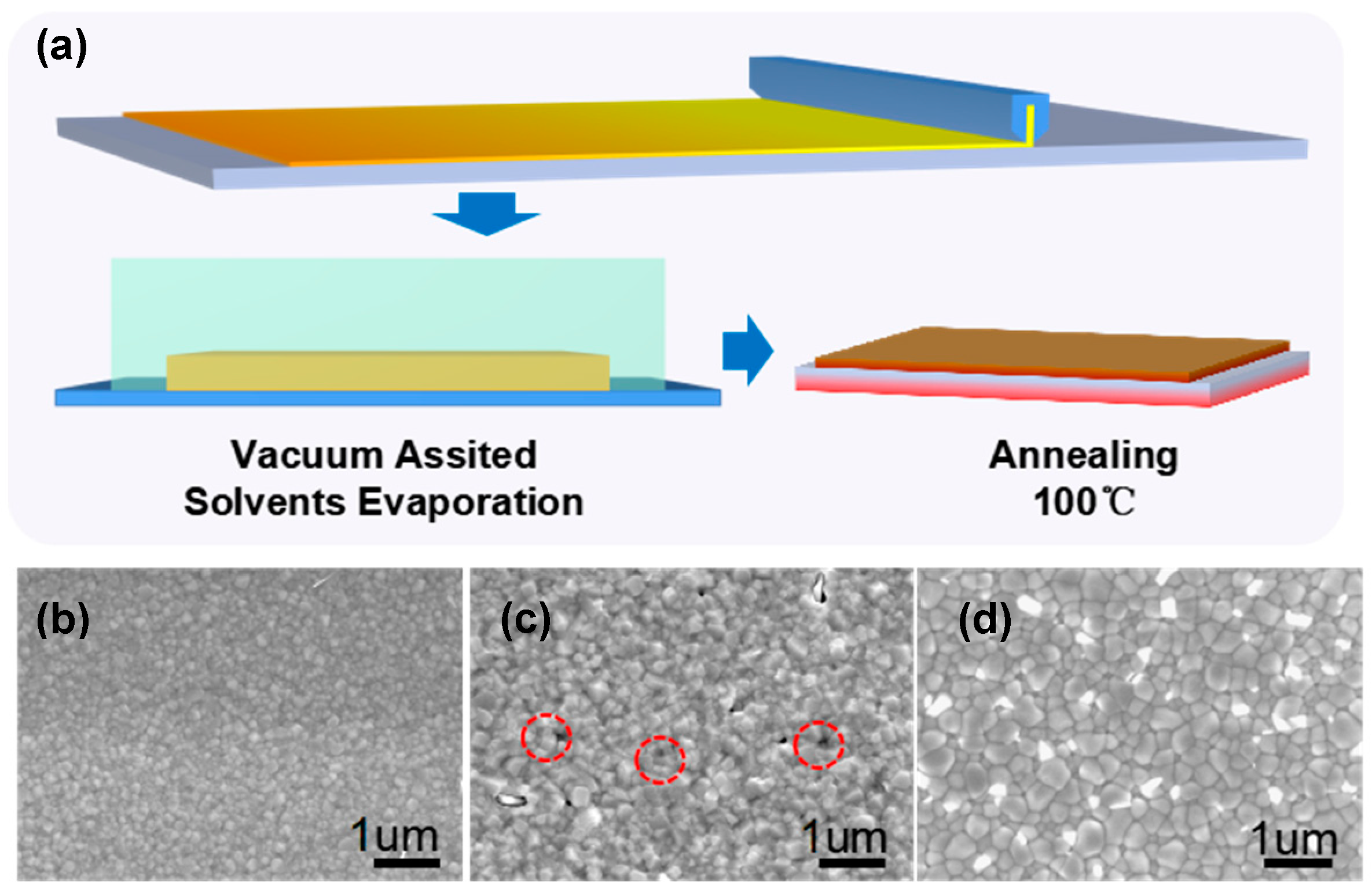
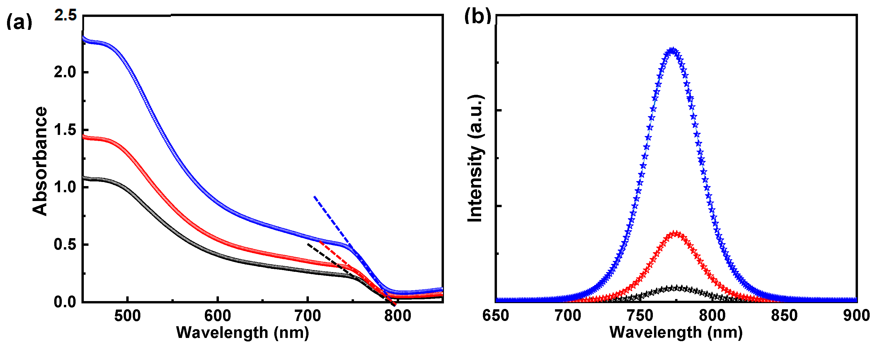
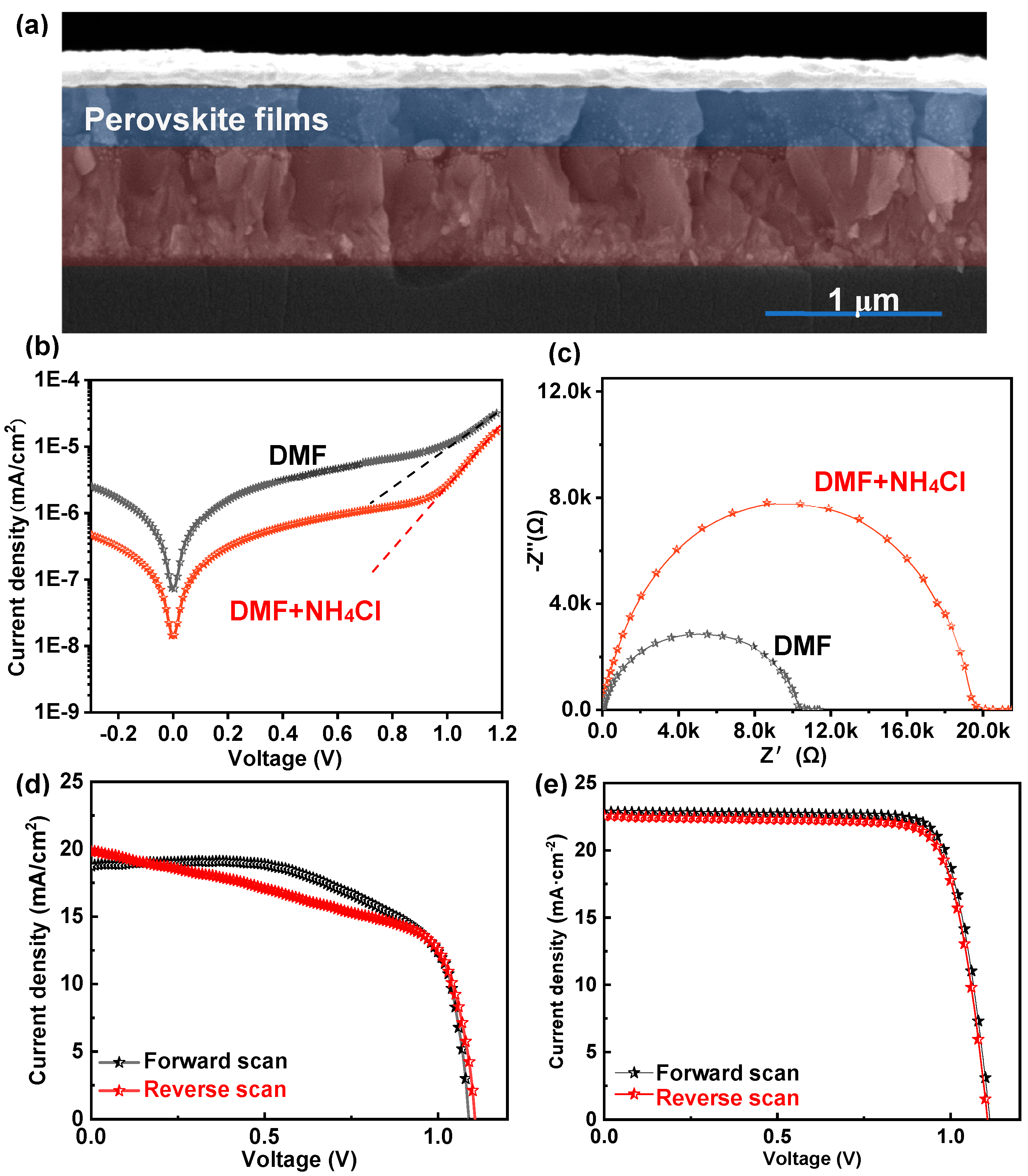
3. Results and Discussion

Currently, the solvent system employed for the preparation of large-area perovskite films via vacuum/nitrogen knife-assisted crystallization blade-coating necessitates the use of volatile solvents at ambient temperature and pressure, such as EtOH and ACN. However, the nucleation and growth processes of perovskite crystals cannot be effectively regulated solely through the use of highly volatile solvents, thereby constraining their applicability in the scalable production of high-quality perovskite films. In this study, we employ EtOH with high volatility as the primary solvent, incrementally incorporating small quantities of DMF and NH4Cl to maintain an adequate volatilization rate. The rapid evaporation of a substantial volume of solvent facilitates the swift and uniform nucleation of perovskite crystals. Concurrently, the formation of a minor DMF/NH4Cl-related intermediate phase within the precursor films enhances the controllability of perovskite crystal growth during the post-annealing process. Based on previous research [4], three kinds of precursor solutions were prepared for this study: EtOH, EtOH + DMF (with a molar ratio of DMF/Pb2+ = 0.8), and EtOH + DMF + NH4Cl (with a molar ratio of NH4Cl/Pb2+ = 0.2). As illustrated in Figure 1a, wet films were initially formed by coating these precursor solutions onto a clean substrate at a coating speed of 20 mm/s in a controlled dry environment (relative humidity RH ≤ 10%). Subsequently, the coated substrates were placed in a vacuum chamber for a brief period of 5 seconds. Then, the samples were removed onto the heating table for a subsequent annealing treatment at 100 °C for a duration of 10 minutes. Figure 1b–d illustrate the surface morphologies of the perovskite thin films synthesized from three distinct precursor solutions.
The perovskite film synthesized from the precursor solution containing solely EtOH exhibits a flat surface and a dense microstructure [28,29]. The grain sizes within the film are uniformly distributed, albeit relatively small, ranging from 50 to 100 nm. This limited grain size is primarily attributed to the rapid volatilization of the solvent and the consequent increase in solution concentration, conditions under which nucleation predominantly occurs within the precursor films. Within a brief duration, a dense microstructure develops in the film, thereby inhibiting the crystal growth process. Concurrently, crystal growth ceases entirely once the solvent has fully volatilized. These factors collectively result in a smooth and compact microstructure of the film, albeit with a small grain size. During this process, the introduction of a minor quantity of DMF facilitates the gradual transformation of the mesophase structure present in the precursor film into a perovskite crystal structure during the post-annealing stage. Concurrently, DMF progressively volatilizes and dissolves the crystal boundaries, leading to the formation of larger crystal particles. Nevertheless, due to the low volatility of DMF, a limited number of voids are observed in the prepared film, as illustrated in Figure 1c. Subsequently, a minor quantity of NH4Cl was introduced into the precursor solution, resulting in an enhancement of the crystal particles within the film. Concurrently, the surface morphology of the film exhibited significant improvement. To further investigate the dynamic process of crystal growth in the perovskite thin film, this study analyzed the crystal structure of three types of perovskite thin films both before and after annealing, utilizing X-ray diffraction spectra, as illustrated in Figure 2a,b.
Figure 2a presents the X-ray diffraction (XRD) spectra of various perovskite films, both before and after annealing at 100 °C for 10 minutes. In the sample devoid of DMF and NH4Cl, the precursor film exhibits only a weak diffraction peak corresponding to the α-phase FAPbI3 perovskite. This indicates the presence of a substantial number of fine α-phase perovskite crystal nuclei within the film. The full width at half maximum (FWHM) of the primary XRD peak associated with the α-phase crystal nuclei is 14.1°, and the crystal nucleus size, as calculated from the FWHM, is approximately 50 nm. With the addition of DMF to the precursor film, the relative integral area of the α-phase perovskite nucleus (100) correlated XRD diffraction peak (approximately 14.1°) progressively decreases. This observation indicates a gradual reduction in the proportion of the α-phase crystal (100) component within the film [4,30,31,32]. Concurrently, a secondary phase diffraction peak emerges between 8° and 9°, which, according to literature reports, is likely attributable to the formation of an intermediate phase resulting from the coordination of DMF with FAPbI3. Upon the addition of a small quantity of NH4Cl to the precursor solution, there is a progressive enhancement in the diffraction peak intensity of the secondary phase relative to the α-phase perovskite crystal nucleus. This indicates an increased relative content of the intermediate phase within the surface precursor film, corroborating the aforementioned analytical results. Post-annealing, the diffraction peaks corresponding to DMF and the intermediate phase are no longer observed, indicating a complete transformation of all products into α-phase perovskite crystals. After adding the NH4Cl, the intensity of the corresponding 14.1° diffraction peak progressively increases, while the half-height width correspondingly decreases. This observation suggests that the size of the perovskite crystals within the film enlarges, corroborating the SEM test results. Consequently, the presence of the intermediate phase appears to facilitate the crystal growth of the perovskite film during the subsequent annealing process.
Subsequently, in light of the aforementioned conclusions, an analysis of the optical properties of perovskite thin films synthesized from the three precursor solutions was conducted. Figure 3a presents the absorption characteristic curve of the perovskite thin film. The absorption spectra of the perovskite thin films, fabricated using a precursor solution with pure EtOH as the primary solvent, predominantly span the range of 450 nm to 800 nm. The intersection of the absorption curve with the X-axis occurs at approximately 780 nm. This observation aligns closely with the absorption characteristic curve of perovskite thin films reported in the literature, suggesting that the thin film primarily comprises α-phase perovskite crystals [31]. Simultaneously, the absorption intensity of the film sample is significantly enhanced by the addition of DMF, primarily due to the increased crystal particle size within the film. Additionally, it was observed that the slope of the absorption edge (approximately 780 nm) in the film’s absorption curve is steeper compared to the aforementioned samples. This phenomenon is predominantly attributed to the effective improvement in the microstructure of the perovskite film following the incorporation of DMF. Furthermore, the absorption intensity of the thin film was significantly enhanced, and the slope of the absorption edge of the absorption curve was also improved following the addition of an appropriate amount of NH4Cl to the precursor solution. This suggests that the incorporation of NH4Cl further optimized the microstructure of the perovskite thin film [33]. Figure 3b presents the photoluminescence curves of the film samples prepared from the three different precursor solutions. The addition of a small amount of DMF and NH4Cl to the precursor solution results in a gradual increase in the luminescence intensity of the thin film sample, suggesting an enhancement in the crystal structure of the synthesized FAPbI3 thin film. This observation aligns with the findings from XRD and SEM analyses, which further corroborate that the incorporation of DMF and NH4Cl in the precursor solution facilitates the improvement of the quality and controllability of FAPbI3 thin films.
To further analyze the effects of DMF and NH4Cl on the microstructure of FAPbI3 films, Figure 4a presents the grain size distribution statistics obtained from SEM images of the thin film samples. It is evident that compared to the FAPbI3 film prepared using a DMF precursor solution, the grain sizes of the sample prepared with an NH4Cl precursor solution are generally larger and exhibit a more concentrated distribution. These findings indicate that the incorporation of DMF and NH4Cl enhances the controllability of perovskite crystal formation, which is advantageous for subsequent scalability. Simultaneously, Atomic Force Microscopy (AFM) images of perovskite films (Figure 4b,c) reveal that the surface roughness of the FAPbI3 film prepared using the NH4Cl precursor solution is lower compared to that of the FAPbI3 film prepared with the DMF precursor solution [34]. Consequently, the flatness of the film surface is enhanced with the addition of NH4Cl, which establishes a foundation for further improving the carrier transport performance of photovoltaic devices. Additionally, Figure 4d presents the cross-sectional Scanning Electron Microscopy (SEM) images of the film samples. The presence of numerous voids at the interface between the FAPbI3 film prepared using a DMF precursor solution and the substrate is evident, which is likely to result in suboptimal carrier transport within photovoltaic devices. Conversely, the incorporation of NH4Cl significantly reduces the voids at the interface of the as-prepared perovskite thin film samples and the substrate. Numerous studies indicate that this phenomenon is primarily attributed to the volatilization of DMF film samples during the annealing process, which leads to the formation of numerous voids at the film’s base. Consequently, the introduction of a small quantity of NH4Cl enhances the interface morphology between the film and the substrate. This improvement is crucial for optimizing carrier transport.
To further investigate the transport properties of carriers in photovoltaic devices, reverse-structure thin film photovoltaic devices were fabricated utilizing the aforementioned perovskite thin films. The architecture of these thin film photovoltaic devices comprises ITO glass/NiO layer (hole transport layer, HTL)/FAPbI3/C60 (electron transport layer, ETL)/BCP/Ag. Cross-sectional SEM images of the photovoltaic device are presented in Figure 5a, with an active area of 0.09 cm2. Figure 5 illustrates the voltage–current characteristics of the photovoltaic device under dark conditions. The data indicate a decrease in the reverse saturation current density with the incorporation of NH4Cl. This observation, when integrated with the analysis of the thin film microstructure, suggests that the addition of NH4Cl mitigates defects within the perovskite thin film. Consequently, this reduction in defects diminishes carrier recombination within the device, thereby enhancing carrier transport properties. These improvements are anticipated to significantly elevate the photovoltaic performance of the perovskite thin film solar cell. Simultaneously, electrochemical impedance spectroscopy (EIS) measurements were conducted (Figure 5c) to evaluate the charge transfer and recombination processes in perovskite solar cells (PSCs) fabricated using various precursor solutions. The charge recombination resistance (Rrec) of the PSC prepared with DMF + NH4Cl was found to be higher than that of the sample prepared with DMF alone, suggesting that the interface characteristics of the thin film photovoltaic devices are substantially improved upon the incorporation of NH4Cl. This result is consistent with the analytical results obtained from the cross-sectional SEM images of the aforementioned thin film samples. Moreover, enhanced charge extraction can contribute to improvements in both the short-circuit current density (Jsc) and the open-circuit voltage (Voc) of photovoltaic devices.
Furthermore, the J–V characteristic curve of the photovoltaic device under AM1.5 illumination is presented in Figure 5d,e, with detailed parameters provided in Table 1. The J–V characteristic curve of the photovoltaic device sample incorporating DMF exhibits a pronounced S-shaped distortion, suggesting inferior photo-generated carrier transportation under illuminated conditions. Under illumination, the photovoltaic device exhibits an open-circuit voltage (VOC) of 1.09 V, a short-circuit current density (JSC) of 18.76 mA/cm2, a fill factor (FF) of 64.80%, and a PCE of 13.25%. After the addition of NH4Cl, the current–voltage (J–V) characteristic curve of the thin film photovoltaic device exhibits a progressive flattening. As a result, the open-circuit voltage increases to 1.1 V, the short-circuit current density rises to 22.86 mA/cm2, and the PCE improves to 20.12%. Simultaneously, the relatively concentrated forward and reverse scanning results of photovoltaic devices with NH4Cl addition suggest a high degree of repeatability in the process method. The observed decrease in photoelectric conversion efficiency may be attributed to an increase in the internal resistance of series cells. In subsequent stages, the photovoltaic efficiency can be enhanced by further adjusting the parameters of the precursor solution and optimizing the interface contact to minimize performance losses. Simultaneously, Figure 6a,b illustrate the statistical power conversion efficiency (PCE) of solar cells fabricated with and without the incorporation of NH4Cl into the precursor solution, based on ten samples prepared under each set of conditions. The results indicate that the PCE of samples prepared without NH4Cl ranges from approximately 4% to 7%, whereas the PCE of samples prepared with NH4Cl ranges from approximately 16% to 21%, and the related parameters are shown in Table S1. These results further demonstrate that the addition of NH4Cl significantly enhances the PCE and repeatability of perovskite thin film solar cells, thereby facilitating the scalable fabrication of PSCs.
Furthermore, we evaluated the operational stability of the photovoltaic device under continuous illumination. To enhance stability, a 20 nm layer of bismuth (Bi) was applied as an inert buffer layer before the evaporation of the silver (Ag) electrode [35,36]. This buffer layer serves to mitigate iodine-induced corrosion of the Ag electrode, which can result from the decomposition and diffusion of perovskite. The maximum power point (MPP) of the photovoltaic device was continuously monitored and assessed using a white LED as the aging light source, with an equivalent light intensity of 1 sun. The module temperature was maintained at 30 ± 5 °C, as depicted in Figure 6. After subjecting the aforementioned small photovoltaic device, with an effective area of 0.09 cm2, to 500 hours of continuous illumination, the photoelectric conversion efficiency of the device incorporating NH4Cl remains at 95.6% of its initial efficiency. In contrast, photovoltaic devices fabricated using DMF exhibit a more pronounced efficiency decay. Consequently, the incorporation of NH4Cl enhances the stability of thin film photovoltaic devices, primarily due to the high-quality, low-defect-density perovskite thin film and the improved carrier transport mechanism at the NiO/C60 stable interface.

4. Conclusions

In this study, high-quality FAPbI3 perovskite thin films were synthesized using a coating method. The incorporation of DMF and NH4Cl enhanced the stability and temporal window of the wet film and moderated the crystal growth rate within the film. This approach increased the content of the intermediate phase in the wet film, allowing perovskite grains to grow further during the annealing process. Consequently, the grain sizes were enlarged, the density of grain boundary defects was reduced, and the crystalline quality of the film was significantly improved.
Furthermore, the interfacial contact between the perovskite film and the substrate is significantly enhanced through the incorporation of liquid DMF and solid NH4Cl. An analysis of the carrier transport mechanism under dark conditions reveals that the high-quality FAPbI3 perovskite thin film, along with the improved interface performance, enhances the carrier transport properties of the corresponding photovoltaic device. Based on these findings, under simulated illumination conditions, the photovoltaic performance parameters of the thin film device were enhanced by the incorporation of a small amount of DMF and NH4Cl, resulting in a photoelectric conversion efficiency of 20.12%. Furthermore, the decay curve of the photoelectric conversion efficiency under continuous irradiation with an equivalent 1-sun white-light source indicates that the improved microstructure of the perovskite thin film achieved through the addition of DMF and NH4Cl also enhances the operational stability of the photovoltaic device. The results indicate that solid Lewis base additives enable the control and scalability of perovskite crystal growth, which is crucial for advancing the industrialization of perovskite thin film photovoltaic devices.

Supplementary Materials

The following supporting information can be downloaded at https://www.mdpi.com/article/10.3390/coatings14091113/s1, Table S1. Related photovoltaic parameters of PSCs fabricated with precursor solutions containing DMF and DMF + CH4Cl.

Author Contributions

Conceptualization, Z.J. and Q.M.; methodology, J.L.; software, Y.Z. (Yufei Zhang) and Y.Z. (Yulong Zhang); validation, B.W.; formal analysis, Z.Q.; investigation, Z.Q.; resources, W.Z.; data curation, R.Z.; writing—original draft preparation, Z.J.; writing—review and editing, Z.J.; visualization, supervision, Z.J.; project administration, K.L. and Q.M. All authors have read and agreed to the published version of the manuscript.

Funding

This research was funded by Taiyuanuniversity of Science and Technology Scientific Research Initial Funding, grant number 20232091, the Fundamental Research Program of Shanxi Provinces (No. 0210302123221), the Fundamental Research Program of Shanxi Provinces (No. 202203021222207), the Fundamental Research Program of Shanxi Province (202103021224268), the Special Fund for Science and Technology Innovation Teams of Shanxi Province (No. 02204051001002), and the Fundamental Research Program of Shanxi Province (No. 202203021221146).

Institutional Review Board Statement

Not applicable.

Informed Consent Statement

Not applicable.

Data Availability Statement

Data are contained within the article/Supplementary Materials; further inquiries can be directed to the corresponding author.

Acknowledgments

We gratefully acknowledge Beihang University and Hangzhou Acme Optoelectronics Technology Co., Ltd. for providing access to their experimental equipment to fabricate samples and their measurements.

Conflicts of Interest

The authors declare that they have no known competing financial interests or personal relationships that could have appeared to influence the work reported in this paper.

References

  1. Kojima, A.; Teshima, K.; Shirai, Y.; Miyasaka, T. Organometal halide perovskites as visible-light sensitizers for photovoltaic cells. J. Am. Chem. Soc. 2009, 131, 6050–6051. [Google Scholar] [CrossRef] [PubMed]
  2. Green, M.A.; Ho-Baillie, A.; Snaith, H.J. The emergence of perovskite solar cells. Nat. Photonics 2014, 8, 506–514. [Google Scholar] [CrossRef]
  3. Green, M.A. Commercial progress and challenges for photovoltaics. Nat. Energy 2016, 1, 15015. [Google Scholar] [CrossRef]
  4. Jiang, Z.; Wang, B.; Zhang, W.; Yang, Z.; Li, M.; Ren, F.; Imran, T.; Sun, Z.; Zhang, S.; Zhang, Y. Solvent engineering towards scalable fabrication of high-quality perovskite films for efficient solar modules. J. Energy Chem. 2023, 80, 689–710. [Google Scholar] [CrossRef]
  5. Chen, R.; Zhang, W.; Guan, X.; Raza, H.; Zhang, S.; Zhang, Y.; Troshin, P.A.; Kuklin, S.A.; Liu, Z.; Chen, W. Rear electrode materials for perovskite solar cells. Adv. Funct. Mater. 2022, 32, 2200651. [Google Scholar] [CrossRef]
  6. Yang, Z.; Zhang, W.; Wu, S.; Zhu, H.; Liu, Z.; Liu, Z.; Jiang, Z.; Chen, R.; Zhou, J.; Lu, Q. Slot-die coating large-area formamidinium-cesium perovskite film for efficient and stable parallel solar module. Sci. Adv. 2021, 7, 3749. [Google Scholar] [CrossRef]
  7. Kam, M.; Zhu, Y.; Zhang, D.; Gu, L.; Chen, J.; Fan, Z. Efficient mixed-cation mixed-halide perovskite solar cells by all-vacuum sequential deposition using metal oxide electron transport layer. Sol. RRL 2019, 3, 1900050. [Google Scholar] [CrossRef]
  8. Deng, Y.; Xu, S.; Chen, S.; Xiao, X.; Zhao, J.J. Huang, Defect compensation in formamidinium–caesium perovskites for highly efficient solar mini-modules with improved photostability. Nat. Energy 2021, 6, 633–641. [Google Scholar] [CrossRef]
  9. Bu, T.; Li, J.; Li, H.; Tian, C.; Su, J.; Tong, G.; Ono, L.K.; Wang, C.; Lin, Z.; Chai, N. Lead halide–templated crystallization of methylamine-free perovskite for efficient photovoltaic modules. Science 2021, 372, 1327–1332. [Google Scholar] [CrossRef]
  10. Feng, Q.; Huang, X.; Tang, Z.; Hou, Y.; Chang, Q.; Nie, S.; Cao, F.; Niu, X.; Yin, J.; Li, J. Governing PbI6 octahedral frameworks for high-stability perovskite solar modules. Energy Environ. Sci. 2022, 15, 4404–4413. [Google Scholar] [CrossRef]
  11. Si, H.; Liao, Q.; Kang, Z.; Ou, Y.; Meng, J.; Liu, Y.; Zhang, Z.; Zhang, Y. Deciphering the NH4PbI3 Intermediate Phase for Simultaneous Improvement on Nucleation and Crystal Growth of Perovskite. Adv. Funct. Mater. 2017, 17, 1701804. [Google Scholar] [CrossRef]
  12. Deng, Y.; Zheng, X.; Bai, Y.; Wang, Q.; Zhao, J.; Huang, J. Surfactant-controlled ink drying enables high-speed deposition of perovskite films for efficient photovoltaic modules. Nat. Energy 2018, 3, 560–566. [Google Scholar] [CrossRef]
  13. Guo, F.; Qiu, S.; Hu, J.; Wang, H.; Cai, B.; Li, J.; Yuan, X.; Liu, X.; Forberich, K.; BrabecC, J. A Generalized Crystallization Protocol for Scalable Deposition of High-Quality Perovskite Thin Films for Photovoltaic Applications. Adv. Sci. 2019, 6, 1901067. [Google Scholar] [CrossRef] [PubMed]
  14. Deng, Y.; Van Brackle, C.H.; Dai, X.; Zhao, J.; Chen, B.; Huang, J. Tailoring solvent coordination for high-speed, room-temperature blading of perovskite photovoltaic films. Sci. Adv. 2019, 5, 7537. [Google Scholar] [CrossRef] [PubMed]
  15. Gao, Y.; Wu, Y.; Lu, H.; Chen, C.; Liu, Y.; Bai, X.; Yang, L.; Yu, W.W.; Dai, Q.; Zhang, Y. CsPbBr3 perovskite nanoparticles as additive for environmentally stable perovskite solar cells with 20.46% efficiency. Nano Energy 2019, 59, 517–526. [Google Scholar] [CrossRef]
  16. Lee, J.W.; Bae, S.H.; Marco, N.D.; Hsieh, Y.T.; Dai, Z.; Yang, Y. The role of grain boundaries in perovskite solar cells. Mater. Today Energy 2018, 7, 149–160. [Google Scholar] [CrossRef]
  17. Wang, B.; Wong, K.Y.; Yang, S.; Chen, T. Crystallinity and defect state engineering in organo-lead halide perovskite for high-efficiency solar cells. J. Mater. Chem. A 2016, 4, 3806–3812. [Google Scholar] [CrossRef]
  18. Huang, F.; Dkhissi, Y.; Huang, W.; Xiao, M.; Benesperi, L.; Rubanov, S.; Rubanov, S.; Zhu, Y.; Lin, X.; Jiang, L.; et al. Gas-assisted preparation of lead iodide perovskite films consisting of a monolayer of single crystalline grains for high efficiency planar solar cells. Nano Energy 2014, 10, 10–18. [Google Scholar] [CrossRef]
  19. Wang, M.; Cao, F.; Deng, K.; Li, L. Adduct phases induced controlled crystallization for mixed-cation perovskite solar cells with efficiency over 21%. Nano Energy 2019, 63, 103867. [Google Scholar] [CrossRef]
  20. Ma, Q.; Zhang, Y.L.; Lu, C.Q.; Zhang, R.; Wang, X.J.; Zhang, W.J.; Jiang, Z.Y. MACl-induced controlled crystallization in sequentially deposited perovskites for high-efficiency and stable perovskite solar cells. Coatings 2023, 13, 1885. [Google Scholar] [CrossRef]
  21. Docampo, P.; HanuschF, C.; Stranks, S.D.; Doblinger, M.; Feckl, J.M.; Ehrensperger, M.; Minar, N.K.; Johnston, M.B.; Snaith, H.J.; Bein, T. Solution Deposition-Conversion for Planar Heterojunction Mixed Halide Perovskite Solar Cells. Adv. Energy Mater. 2014, 4, 1400355. [Google Scholar] [CrossRef]
  22. Chen, J.; Zuo, L.; Zhang, Y.; Lian, X.; Fu, W.; Yan, J.; Li, J.; Wu, G.; Li, C.Z.; Chen, H. High-Performance Thickness Insensitive Perovskite Solar Cells with Enhanced Moisture Stability. Adv. Energy Mater. 2018, 8, 1800438. [Google Scholar] [CrossRef]
  23. Zhang, Y.; Jiang, Z.; Zhang, W.; Yan, L.; Lu, C.; Ni, C. Pre-crystallization applied in two-step spin-coating method for high-quality perovskite films in photovoltaic devices. J. Alloys Compd. 2020, 832, 153616. [Google Scholar] [CrossRef]
  24. Zhao, Y.; Duan, J.; Wang, Y.; Yang, X.; Tang, Q. Precise stress control of inorganic perovskite films for carbon-based solar cells with an ultrahigh voltage of 1.622 V. Nano Energy 2020, 67, 104286. [Google Scholar] [CrossRef]
  25. Liu, J.; Zhu, L.; Xiang, S.; Wei, Y.; Xie, M.; Liu, H.; Li, W.; Chen, H. Growing high-quality CsPbBr3 by using porous CsPb2Br5 as an intermediate: A promising light absorber in carbon-based perovskite solar cells. Sustain. Energy Fuels 2019, 3, 184–194. [Google Scholar] [CrossRef]
  26. Liu, X.; Liu, Z.; Ye, H.; Tu, Y.; Sun, B.; Tan, X.; Shi, T.; Tang, Z.; Liao, G. Novel efficient C60-based inverted perovskite solar cells with negligible hysteresis. Electrochim. Acta 2018, 288, 115–125. [Google Scholar] [CrossRef]
  27. Teng, P.; Han, X.; Li, J.; Xu, Y.; Kang, L.; Wang, Y.; Yang, Y.; Yu, T. Elegant Face-Down Liquid-Space-Restricted Deposition of CsPbBr3 Films for Efficient Carbon-Based All-Inorganic Planar Perovskite Solar Cells. ACS Appl. Mater. Inter. 2018, 10, 9541. [Google Scholar] [CrossRef]
  28. Luo, J.; Jia, C.; Wan, Z.; Han, F.; Zhao, B.; Wang, R. The novel dopant for hole-transporting material opens a new processing route to efficiently reduce hysteresis and improve stability of planar perovskite solar cells. J. Power Sources 2017, 342, 886–895. [Google Scholar] [CrossRef]
  29. Shi, D.; Adinolfi, V.; Comin, R.; Yuan, M.; Alarousu, E.; Buin, A.; Chen, Y.; Hoogland, S.; Rothenberger, A.; Katsiev, K.; et al. Low trap-state density and long carrier diffusion in organolead trihalide perovskite single crystals. Science 2015, 347, 519–522. [Google Scholar] [CrossRef]
  30. Xiao, Z.; Dong, Q.; Bi, C.; Shao, Y.; Yuan, Y.; Huang, J. Solvent Annealing of Perovskite-Induced Crystal Growth for Photovoltaic-Device Efficiency Enhancement. Adv. Mater. 2014, 26, 6503–6509. [Google Scholar] [CrossRef]
  31. Li, L.; Chen, Y.; Liu, Z.; Chen, Q.; Wang, X.; Zhou, H. The additive coordination effect on hybrids perovskite crystallization and high-performance solar cell. Adv. Mater. 2016, 28, 9862–9868. [Google Scholar] [CrossRef] [PubMed]
  32. Saliba, M.; Etgar, L. Current density mismatch in perovskite solar cells. ACS Energy Lett. 2020, 5, 2886–2888. [Google Scholar] [CrossRef]
  33. Zhang, Y.L.; Jiang, Z.Y.; Li, J.C.; Meng, G.X.; Guo, J.J.; Zhang, W.J. Preparation of efficiency and stability all-inorganic CsPbBr3 perovskite solar cells by pre-crystallization multi-step spin coating method. Coatings 2024, 14, 918. [Google Scholar] [CrossRef]
  34. Li, M.; Li, B.; Cao, G.; Tian, J. Monolithic MAPbI3 films for high-efficiency solar cells via coordination and a heat assisted process. J. Mater. Chem. A 2017, 40, 21313–21319. [Google Scholar] [CrossRef]
  35. Qiu, J.J.; Yang, T.T.; Li, Y.F.; Qian, W.H.; Liu, X.Y. Au@Ag@Pt core–shell nanorods regulating Ag release behavior endow titanium antibacterial activity and biocompatibility. Rare Met. 2022, 41, 630–638. [Google Scholar] [CrossRef]
  36. Aristidou, N.; Eames, C.; Sanchez-Molina, I.; Bu, X.; Kosco, J.; Islam, M.S.; Haque, S.A. Fast oxygen diffusion and iodide defects mediate oxygen-induced degradation of perovskite solar cells. Nat. Commun. 2017, 8, 15218. [Google Scholar] [CrossRef]
Figure 1. (a) Schematic illustration of the coating process for perovskite films. Top-view SEM images of the annealed perovskite films prepared (b) without the additives and with (c) DMF and (d) DMF + NH4Cl.
Coatings 14 01113 g001
Figure 2. (a) X-ray diffraction (XRD) patterns of unannealed perovskite films without the additives (black curve) and with DMF (red curve) and DMF + NH4Cl (blue curve); (b) X-ray diffraction (XRD) patterns of annealed perovskite films without the additives (black curve) and with DMF (red curve) and DMF + NH4Cl (blue curve).
Coatings 14 01113 g002
Figure 3. (a) Absorption spectra of the annealed perovskite films on glasses without the additives (black curve) and with DMF (red curve) and DMF + NH4Cl (blue curve). (b) Photoluminescence (PL) spectroscopy of annealed perovskite films on glasses without the additives (black curve) and with DMF (red curve) and DMF + NH4Cl (blue curve).
Coatings 14 01113 g003
Figure 4. (a) Statistical grain size of perovskite crystals in the annealed films prepared with DMF and DMF + NH4Cl. Atomic force microscope (AFM) images of the annealed perovskite films with (b) DMF and (c) DMF + NH4Cl. (d) Cross-SEM images of the annealed perovskite films with DMF and DMF + NH4Cl.
Coatings 14 01113 g004
Figure 5. (a) Cross-SEM images of the prepared perovskite film solar cells. (b) Dark J–V curves of the PSCs prepared with DMF and DMF + NH4Cl. (c) Nyquist plots of the PSCs prepared with DMF and DMF + NH4Cl in the frequency range of 20 kHz to 0.1 kHz under standard sunlight irradiation (100 mW/cm2) at a bias voltage of 0.8 V. J–V curves for the champion PSCs prepared with (d) DMF and (e) DMF + NH4Cl.
Coatings 14 01113 g005
Figure 6. PCE distribution of PSCs (ten samples) fabricated precursor solutions contained (a) DMF and (b) DMF + NH4Cl. (c) Operational stability of the PSCs exposed under continuous 1 sun illumination (the light source for the aging test was achieved by a 1-sun equivalent white-light LED array) with MPP tracking in dry air (RH ≤ 10%).
Coatings 14 01113 g006
Table 1. Photovoltaic parameters of the champion PSCs fabricated with precursor solutions containing DMF and DMF + NH4Cl.
JSC
(mA/cm2)
VOC
(V)
FF
(%)
PCE (%)
DMFForward scan18.761.0964.8%13.25%
Reverse scan19.901.1059.6%13.05%
DMF + NH4ClForward scan22.861.1179.3%20.12%
Reverse scan22.461.1079.9%19.74%
Disclaimer/Publisher’s Note: The statements, opinions and data contained in all publications are solely those of the individual author(s) and contributor(s) and not of MDPI and/or the editor(s). MDPI and/or the editor(s) disclaim responsibility for any injury to people or property resulting from any ideas, methods, instructions or products referred to in the content.

