Article

Influence of Different Chemical Methods Used for the Deposition of CdSe/ZnO Layers

by
Gediminas Jakubauskas
,
Edita Paluckiene
,
Egle Usoviene
and
Neringa Petrasauskiene
*
Department of Physical and Inorganic Chemistry, Kaunas University of Technology, Radvilenu 19, 50254 Kaunas, Lithuania
*
Author to whom correspondence should be addressed.
Coatings 2025, 15(4), 415; https://doi.org/10.3390/coatings15040415
Submission received: 7 March 2025 / Revised: 28 March 2025 / Accepted: 29 March 2025 / Published: 31 March 2025

Abstract

:
The present study employed the spin-coating method for the preparation of nanostructured crystalline zinc oxide (ZnO) thin films on FTO glass substrates. Subsequently, cadmium selenide (CdSe) layers were deposited on the surfaces using two distinct chemical methods: successive ionic layer adsorption and reaction (SILAR) and chemical bath deposition (CBD). The obtained films were then characterized by a variety of analytical methods, including XRD, SEM, AFM, EDX spectroscopy, UV–vis spectrophotometry, and linear sweep voltammetry. The XRD and SEM studies demonstrated that all of the films exhibited a polycrystalline nature, with the crystallinity of the cadmium selenide thin films prepared using the SILAR method exceeding that obtained by the CBD method. The SEM and AFM images revealed the uniformity of the cadmium selenide films on the FTO substrates, with no visible cracks or pores. The EDX spectra confirmed the presence of the expected elements in the thin films. The optical band gaps (Eg) for CdSe prepared with the SILAR or CBD method were determined to be 1.85 and 1.97 eV, respectively.

1. Introduction

The transition to renewable energy sources as sustainable alternatives to finite and polluting fossil fuels is a key area of contemporary research. The depletion of fossil fuel reserves, together with the pressing necessity for technological advancements to accommodate the increasing demand for energy, has resulted in higher fuel costs and considerable environmental challenges. Consequently, there is a strong impetus to develop innovative, sustainable, and cost-effective energy solutions to support a resilient energy economy.
Photoelectrochemical cells (PECs) have emerged as a promising technology due to their low production costs, environmental friendliness, and simple manufacturing processes. PECs are devices that convert solar radiation into useful electricity. This clean and renewable energy source is a critical component of efforts to mitigate climate change and promote sustainability. Recent research has focused on the development of low-cost photoelectrodes to improve the performance of PECs [1,2,3,4]. To ensure optimal photoconversion efficiency, PEC photoelectrodes must exhibit critical properties such as high quantum efficiency, appropriate band alignment, effective solar absorption, robust and stable semiconductor materials, long-term corrosion resistance, and efficient charge separation mechanisms [1,2].
In recent years, significant interest has been directed towards inorganic semiconductor sensitized solar cells. Metal oxide nanostructures have emerged as a promising platform for photoelectrochemical applications due to their advantageous properties, including high stability, low fabrication cost, and non-toxicity [1,3]. Among the various metal oxide nanostructures, ZnO has garnered particular attention due to its exceptional electrical conductivity and remarkable light absorption capabilities, making it a highly suitable candidate for use as a photoanode [2,3,4] and in quantum dot sensitized solar cells [4,5]. ZnO is classified as an n-type semiconductor, exhibiting higher electron mobility (115–155 cm2 V−1s−1) and a substantial exciton binding energy (60 MeV). Its widespread use as a photocatalyst is well documented [6,7,8]. However, its practical efficiency is constrained by the rapid electron hole recombination (e/h⁺), which diminishes its photocatalytic performance. This limitation stems from the wide band gap energy (3.1–3.4 eV) of ZnO, which restricts its light absorption to the ultraviolet region, coupled with high charge recombination rates that impede efficient solar energy conversion. To mitigate this limitation, a prevalent strategy involves integrating ZnO with other materials to engineer composite photocatalyst systems, thereby augmenting their photocatalytic efficiency. The integration of these hybrid systems has been shown to enhance charge carrier separation and mobility, significantly boosting the photocatalytic activity of ZnO [9,10].
The photoelectrochemical performance of photoanodes can be enhanced by incorporating a metal chalcogenide, such as CdSe, which has a smaller band gap, thereby extending light absorption into the visible spectrum. Cadmium selenide (CdSe), a binary II–VI semiconductor with a narrower band gap of about 1.7 eV, is a highly efficient light absorber capable of capturing a significant portion of the solar spectrum. It exhibits excellent optoelectronic properties, high stability, and low fabrication cost, thereby improving the PEC photoconversion efficiency of PECs [9]. CdSe is an n-type semiconductor that is distinguished by its remarkable chemical stability and extensive utilization in diverse applications, including photovoltaic cells [10], light-emitting diodes (LEDs) [11], photoelectrochemical cells [1,10], sensor devices [11], and solar cells [6,7,12]. CdSe exhibits a high absorption coefficient (α = 104 cm−1 at 720 nm) [13], which allows the CdSe solar cell to require only a very thin (~ 2 µm) film to absorb sunlight, thus enhancing power conversion efficiency [14].
CdSe/ZnO heterostructures have emerged as a promising material system for optoelectronic applications, exhibiting distinct advantages over other commonly studied systems, such as Si/ZnO [15] and GaN/ZnO [16]. CdSe, with its narrower band gap, exhibits strong absorption in the visible light range, rendering it more efficient for light harvesting in solar cells and photodetectors. Conversely, Si, with its larger band gap, and GaN, with limited visible absorption, are less effective for visible light-driven applications. Furthermore, the observation that CdSe/ZnO exhibits favorable band alignment has been demonstrated to facilitate efficient charge transfer and enhance device performance. Moreover, CdSe’s compatibility with low-temperature, solution-based processing methods stands in contrast to the high-temperature requirements of Si and GaN, which are often more challenging to process. The distinctive properties of CdSe/ZnO heterostructures position them as a promising candidate for next-generation optoelectronic devices.
The combination of ZnO with CdSe has been shown to result in the formation of heterojunction photoanodes, which have been demonstrated to enhance charge separation, light absorption, photocatalytic activity, and stability. This, in turn, has been observed to lead to improved photoelectrochemical performance and increased electron-hole pair generation [1,17]. The interface between ZnO and CdSe is predicted to form a type II band alignment (Figure 1), thus facilitating the transfer of electrons from the conduction band of CdSe to ZnO, while holes migrate from the valence band of ZnO to CdSe. ZnO functions as an efficient electron transport layer due to its high electron mobility, while CdSe absorbs visible light and generates charge carriers [18,19].
Conductive fluorine-doped tin oxides (FTO) are frequently utilized as substrate materials for the deposition of semiconductor films. FTO possesses a substantial band gap (~3.86 eV) [20], which leads to a significantly reduced intrinsic conductivity compared to metals or carbon materials.
The direct fabrication of nanostructured arrays on FTO glass offers several key advantages. These include a high active surface area for semiconductor devices, a full penetration of the nanoarray by the electrolyte, and a strong interface between the photocatalyst and the substrate, allowing for efficient and rapid charge transfer.
The deliberate integration of ZnO and CdSe layers on FTO substrates has been shown to enhance light absorption and charge transport. This integration also provides a flexible foundation for creating efficient and cost-effective optoelectronic devices.
A variety of methodologies have been examined to deposit CdSe and ZnO layers on FTO substrates [3]. These methodologies include, but are not limited to, chemical bath deposition [21,22], successive ionic layer adsorption and reaction [7,23], hydrothermal [24], and electrodeposition [22,23,25]. Each technique possesses distinct advantages with respect to material quality, cost efficiency, and scalability.
In this study, we have presented a synthesized CdSe/ZnO heterostructure on the FTO surface. The spin-coating method was used to prepare nanostructured crystalline ZnO thin films on FTO glass substrates. Subsequently, CdSe layers were deposited on the surfaces by two different chemical methods: successive ionic layer adsorption and reaction (SILAR) and chemical bath deposition (CBD). The resulting samples were characterized using a variety of analytical methods, including X-ray diffraction analysis (XRD), UV–vis spectrophotometry, scanning electron microscopy (SEM), atomic force microscopy (AFM), and energy-dispersive X-ray spectroscopy (EDX). Finally, the photocatalytic properties of the samples were investigated under ultraviolet and visible light using linear sweep voltammetry (LSV).

2. Materials and Methods

2.1. Materials

The chemicals used in this study, including ZnO nanoparticles with a diameter of less than 100 nm, Cd(CH3COO)2, Na2SO3, powdered selenium, and ethanol, were obtained from Sigma-Aldrich (Hamburg, Germany) and utilized without further modification. The FTO (fluorine-doped tin oxide, TEC 10, with a thickness of 3.2 mm and a resistivity of 12 Ω/sq,) glass was obtained from Ossila (Sheffield, UK). The 20 mm × 15 mm FTO substrates were subjected to an ultrasonic cleaning process, followed by a sequence of washes with soap solution, ethanol, and distilled water. The substrates were then dried at 100 °C.

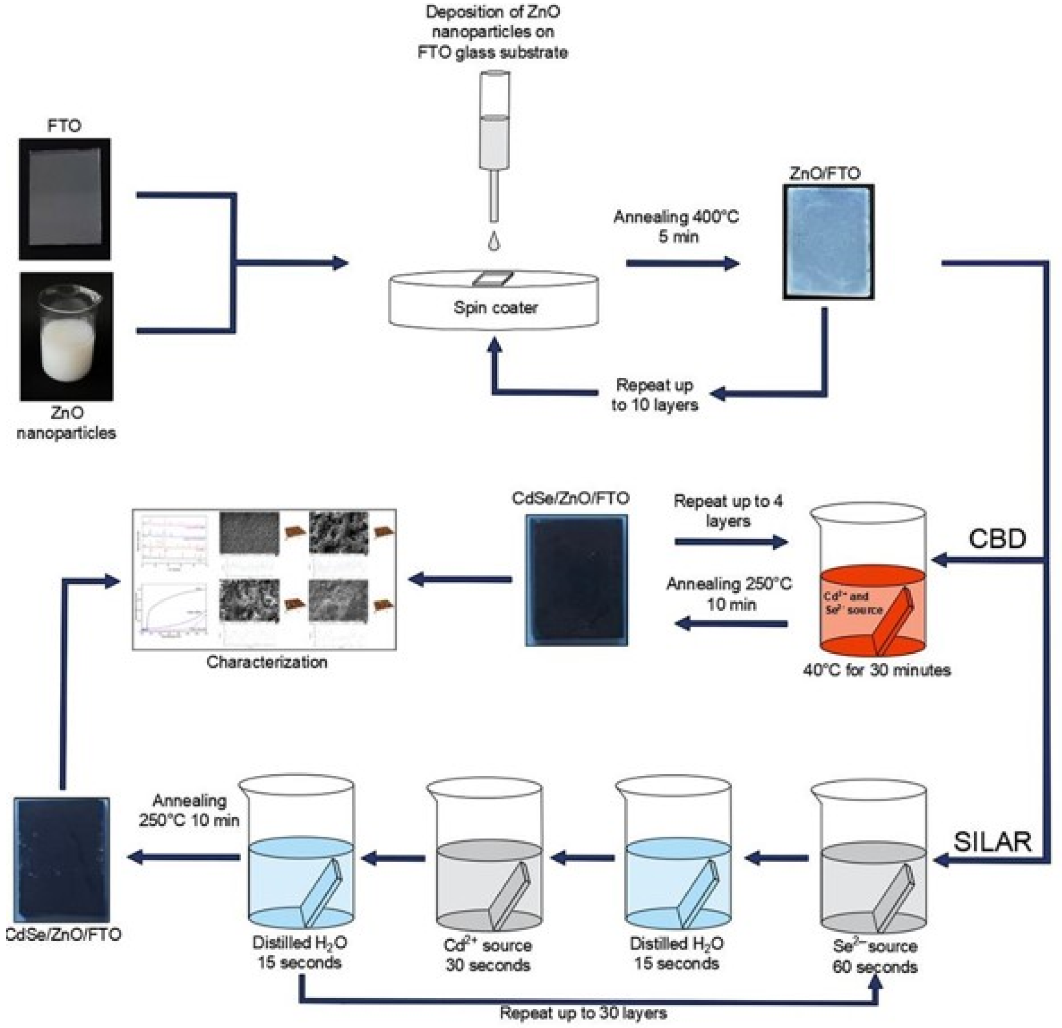
2.2. Formation of ZnO Layers on FTO Substrates

The spin-coating process was employed to deposit the ZnO layers on the FTO substrates. The suspension of zinc oxide nanoparticles was achieved by ultrasonically (using a Sono Swiss SW3H ultrasonic cleaner, Sonoswiss AG, Ramsen, Switzerland) dispersing the ZnO nanoparticles in pure ethanol (0.2 g (ZnO)/10 mL (C2H5OH)). The mixture was stirred for 30 min at room temperature to obtain a homogeneous suspension. The nanoparticle suspension was then subjected to a spin-coating process (using a spin-coating apparatus, SPS SPIN 150, SPS-Europe, Putten, The Netherlands) on the FTO substrates at room temperature for a duration of 30 s at an angular velocity of 2000 rpm. Samples were prepared with 10 cycles of deposited ZnO nanoparticle layers. For each cycle, the FTO glass substrates coated with ZnO layers were subjected to annealing (using a Binder BD APT.LINE incubator, Binder GmbH, Tuttlingen, Germany) for 5 min at a temperature of 400 °C, as illustrated in Figure 2. This process was intended to enhance layer stability, improve adhesion, and induce crystallization.

2.3. Formation of CdSe/ZnO Thin Films on FTO Substrates Using CBD and SILAR

Cadmium selenide thin films were deposited on the FTO substrates with a ZnO layer via two distinct methods, SILAR and CBD, as illustrated in Figure 2.
SILAR is a cost-effective and versatile technique for depositing thin films of controlled thickness and composition on a variety of substrates. It involves the sequential immersion of substrates in precursor solutions, interspersed with rinsing and drying steps. Cadmium acetate (Cd(CH3COO)2) was used as the cation source, while sodium selenosulfate (Na2SeSO3), prepared by dissolving selenium powder in sodium sulfite solution, served as the anion source. The Na2SeSO3 solution was stirred at 80 °C for 8–10 h, filtered, and stored at 4 °C to prevent decomposition. A SILAR cycle consists of (1) Immersion of the substrate in Na2SeSO3 to allow anion adsorption; (2) rinsing with deionized water; (3) immersion in Cd(CH3COO)2 for cation deposition; and (4) a final rinse. This process was repeated for 30 cycles to deposit CdSe thin films on the ZnO/FTO substrates. The films were subsequently annealed at 250 °C for 10 min to enhance crystallinity and reduce defects.
CBD represents a low-cost, scalable method of depositing uniform thin films on large substrates. The process entails subjecting a substrate to an immersion in a solution containing metal ions and a complexing agent, which facilitates the formation of a thin film. The deposition of CdSe thin films on FTO glass was achieved through the use of cadmium acetate, sodium selenosulfate, EDTA, and deionized water. The Cd2⁺ and Se2− ions were gradually released and condensed on the ZnO-coated FTO substrates within a reaction bath maintained at 40 °C for a duration of 30 min. Subsequently, the films underwent a thermal annealing process at a temperature of 250 °C for a period of 10 min. It is noteworthy that the completion of the coating process required the execution of four deposition-annealing cycles.
The color of the CdSe thin films, obtained by either the SILAR or the CBD method, undergoes a transition from white to dark brown, indicative of the formation of a CdSe thin film.

2.4. Characterization of CdSe/ZnO Structure

An X-ray diffractometer (D8 Advance diffractometer, Bruker AXS, Karlsruhe, Germany) was used to analyze the crystal phase of the CdSe/ZnO samples, and the observed peaks were then compared with those available in the PDF-2 database. The experimental interplanar spacing (d-values) for ZnO and CdSe was determined using the Bragg relation [26], which is derived from the θ value of the peak in the XRD pattern:
n λ = 2 d   s i n θ .
In this equation, n (an integer) denotes the order of diffraction, λ signifies the wavelength of the incident X-rays, d represents the interplanar spacing of the crystal, and θ designates the position of the peak. The mean crystallite size (D) was determined by calculation based on the full width at half maximum (FWHM) intensity of the primary reflections by applying the Debye–Scherrer formula [27,28]:
D = 0.9 λ β c o s θ ,
where D is the crystallite size, λ indicates the wavelength of X-rays, and β denotes the full width at half maximum (FWHM) intensity in radians.
Scanning electron microscopy/energy-dispersive X-ray spectroscopy (SEM/EDX) measurements were performed using a Hitachi S-3400N microscope (Hitachi Ltd., Mito Works, Hitachinaka City, Ibaraki Prefecture, Japan), which was equipped with the Bruker Quad 5040 EDS system.
The atomic force microscope (AFM) NanoWizard®3 (JPK Instruments, Bruker Nano GmbH, Berlin, Germany) was utilized for the purpose of conducting a thorough examination of the surface characteristics of the CdSe/ZnO/FTO samples. The operation of the AFM was carried out in contact mode, using an I-shaped silicon cantilever with a radius of curvature of less than 10.0 nm and a cone angle of 20°.
The optical properties of the CdSe/ZnO samples were analyzed at room temperature using a SPECTRONIC® GENESYS8 UV–vis spectrometer (Perkin Elmer, Waltham, MA, USA) in the 350 to 700 nanometer range. The optical band gap was calculated from diffuse absorbance measurements using the Tauc plot [29,30]:
( α h υ ) 1 / n = A ( h υ E g )
In this equation, α is the absorption coefficient; hν—photon energy; Eg—energy band gap; A—a constant; and n—a constant for a given transition (n = 2 for the direct transition). The optical band gap can be estimated by extrapolating the linear part of the plots of (αhν)2 versus hν to α = 0.
The active surface area was measured by linear sweep voltammetry (LSV), with the BioLogic SP-150 potentiostat–galvanostat (BioLogic Science Instruments, Seyssinet-Pariset, France). The experimental data were collected and processed using the EC-Lab® V10.39 software. The experimental setup comprised a standard three-electrode cell, with a volume of 100 milliliters, and the following composition for the electrodes: platinum wire as the counter electrode, Ag,AgCl|KCl(sat) as the reference electrode, and CdSe/ZnO formed on FTO as the working electrode. The supporting electrolyte used in this study was a 0.1 M sodium thiosulfate solution, with a pH of 6.3. A General Electric F8W/BLB lamp (GE Lighting, Cleveland, USA) (λmax = 366 nm, with a determined average irradiance p = 1.8 mW·cm−2), mounted at a distance of 2 cm from the surface of the working electrode, was used as the UV radiation source for the linear sweep voltammetry measurements. During the process of performing LSV measurements, the potential was swept from −0.4 to + 1.0 V within the frequency range of 5 kHz to 50 Hz with a sinusoidal amplitude of 10 mV.

3. Results and Discussion

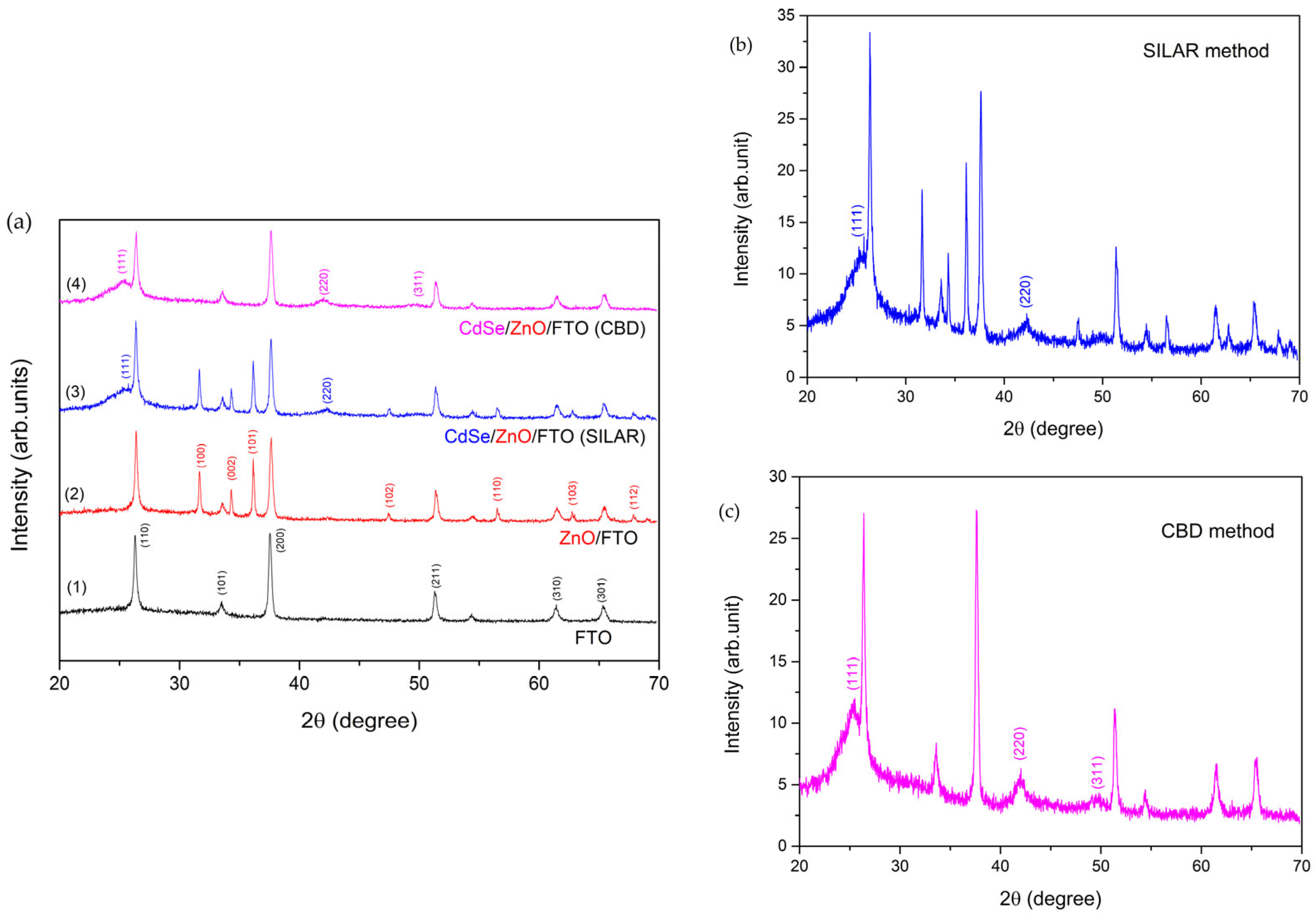
3.1. Structural Studies

An investigation was conducted into the crystal structures of the ZnO and CdSe/ZnO heterostructures deposited on FTO by different chemical methods. The X-ray diffraction patterns were analyzed, and the results are presented in Figure 3. The X-ray diffraction results indicate that the films have a polycrystalline structure.
As illustrated in Figure 3, four distinct sets of diffraction peaks can be observed for a CdSe/ZnO thin film on FTO, corresponding to tetragonal rutile SnO2, hexagonal wurtzite ZnO, and cubic CdSe. These results indicate that ZnO and CdSe were the primary components of the thin film. The diffraction peaks associated with FTO appear at 2θ values of 26.78°, 33.96°, 37.98°, 51.75°, 61.99°, and 65.82° (Figure 3a(1 curve)), corresponding to the (110), (101), (200), (211), (310), and (301) crystal planes of tetragonal cassiterite SnO2, respectively. These peaks align with the standard reference card (JCPDS No. 71-0652), and no additional diffraction peaks beyond those of polycrystalline SnO2 were detected.
In Figure 3a(2 curve), the XRD pattern for polycrystalline ZnO displays distinct diffraction peaks that correspond to the hexagonal wurtzite structure. This result is consistent with the literature (JCPDS No. 36-1451). Notable ZnO diffraction peaks were identified at 2θ angles of 31.94°, 34.61°, 36.42°, 47.94°, 57.05°, 63.29°, and 68.37°, which are related to different crystal facets such as (100), (002), (101), (102), (110), (103), and (112) [7,19,31]. In the figure, these peaks are sharp and narrow, indicating well-defined crystallinity and asymmetry in the crystalline forms. The diffraction peaks of other aspects such as (102), (110), (103), and (112), are almost invisible due to their essentially very low intensity, which is almost less than 0.5% of the maximum intensity peak. The intensity of the (002) peak does not show a dominant enhancement compared to the (100) and (101) peaks, indicating the absence of a strong preferential c-axis orientation [32]. This indicates random polycrystalline growth, which is expected for ZnO films synthesized by low-temperature chemical methods where substrate-driven alignment is less pronounced. The Scherrer equation (Equation (2)) was used to estimate the crystallite size of ZnO from a diffraction peak at 2θ ~36.42°, corresponding to the (101) plane. This analysis yielded an average crystallite size of 44 nm for ZnO.
During the process of forming a CdSe/ZnO heterostructure, the diffraction peaks of ZnO were slightly suppressed when CdSe was deposited on ZnO (Figure 3). This observation indicates that CdSe modified the interface of ZnO. The diffractograms of the XRD pattern of thin CdSe/ZnO films obtained by depositing CdSe on the surface of ZnO/FTO using the SILAR method (Figure 3a(3 curve),b) show two new broad peaks at values of 2θ = 25.37° and 42.03°, corresponding to the lattice planes (111) and (220), respectively. The presence of these peaks indicates the occurrence of heterogeneous growth of CdSe on the ZnO nanostructure, thereby suggesting a successful deposition of CdSe on ZnO, resulting in the formation of the CdSe/ZnO heterostructure. The results obtained demonstrate that CdSe was obtained in a cubic crystal structure, which is consistent with the literature (JCPDS card No. 19-0191) [33,34,35]. The broadness of the peaks is likely attributable to the fine grain size.
The sample obtained by depositing CdSe on ZnO/FTO by the CBD method (see Figure 3a(4 curve),c) showed an additional characteristic peak at a value of 49.76°, which corresponds to the diffraction of the (311) plane of the cubic CdSe phase.
The crystallite size of CdSe was determined by analyzing the planes (111) and (220) of the cubic phase. For the CdSe layers obtained by depositing CdSe on the surface of ZnO/FTO, a crystallite size of ~ 10 nm was estimated for both deposition methods, SILAR and CBD. This finding is consistent with previous reports documenting similar crystallite sizes for CdSe layers deposited via chemical methods on FTO glass substrates [7,23,25].
The absence of impurity peaks in the XRD patterns indicates the formation of a pure CdSe/ZnO thin film. It is noteworthy that the diffraction peaks observed in the ZnO/FTO structure were more pronounced (Figure 3a(2 curve)), while the diffraction peaks of CdSe/ZnO were wider and weaker (Figure 3b,c), suggesting that ZnO is more crystalline than the resulting CdSe coating. A comparison of the SILAR and CBD methods reveals that the SILAR method produced slightly less crystalline cadmium selenide. This phenomenon can be attributed to the reagents utilized in the SILAR method, which do not allow sufficient time for the nucleation process of cadmium selenide crystallization to occur, thereby slowing down this process in the SILAR method relative to that of the CBD method.
The results of the XRD analysis were compared with the JCPDS data, and the findings are presented in Table 1.

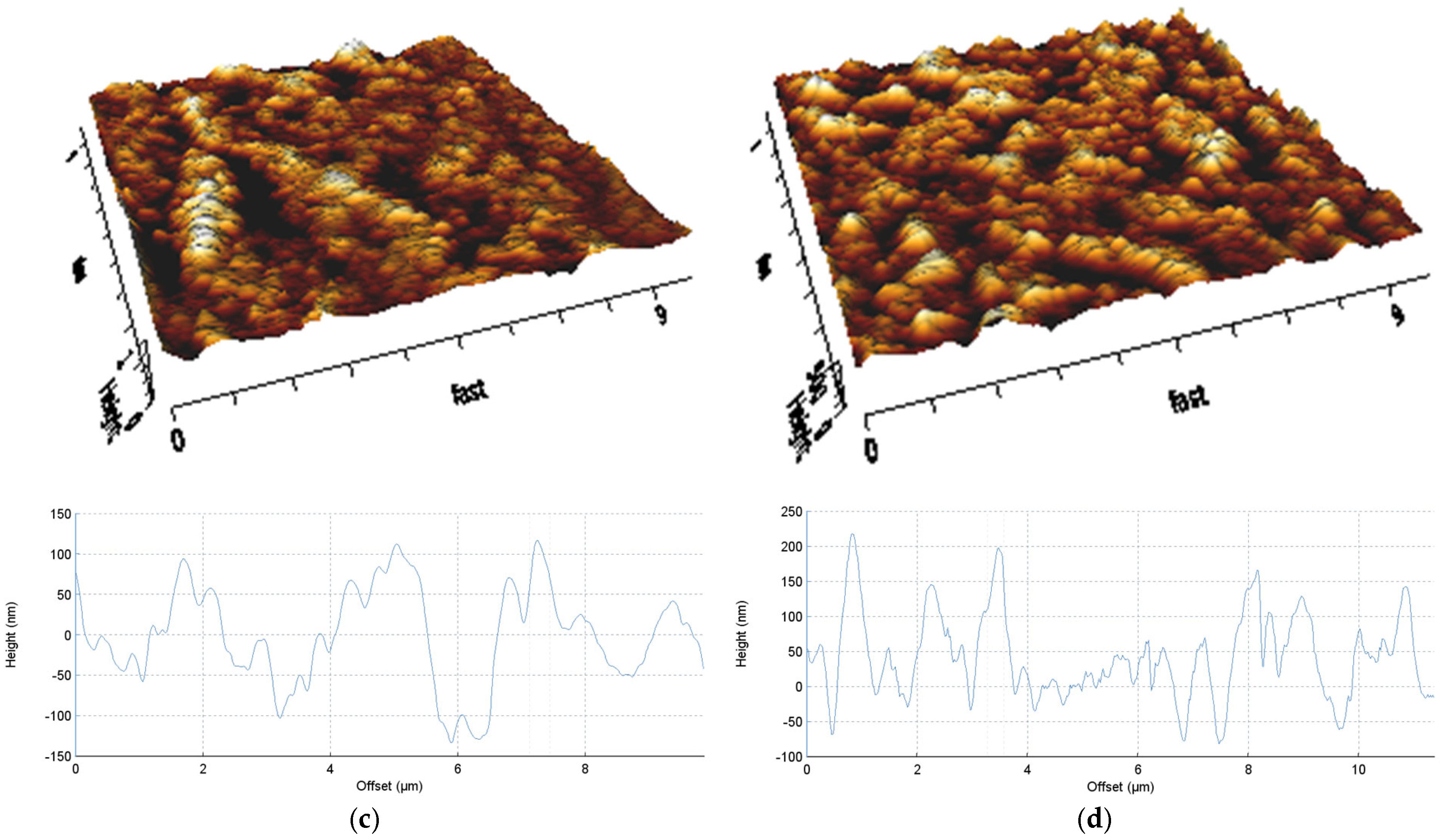
3.2. Morphological Analysis

The morphology of the ZnO thin films before and after deposition of CdSe layers was evaluated by SEM and AFM. SEM images of pristine FTO and ZnO/FTO are shown in Figure 4. The surface of FTO (Figure 4a) is composed of fine crystallites of uniform size, which are evenly distributed over the scanned area. However, the deposition of ZnO nanoparticles on the surface of FTO resulted in a significant change in surface morphology, as shown in Figure 4b. The scanned area exhibited a novel, porous, and reticulated structure composed of small, uniformly sized crystallites. SEM images unequivocally demonstrate that the FTO substrate was completely covered with a ZnO layer.
AFM images (10 μm × 10 μm) and profiles of the pristine surfaces of FTO and ZnO are shown in Figure 5.
The cross-sectional profilogram illustrates the dimensions of each component on the surface structure, as well as the recurring patterns of elevations and depressions. A topographic view of the FTO surface (top of Figure 5a) shows that it is composed of evenly spaced small elevations and depressions, and the arrangement of the structural elements in the topographic image of the surface is the same as in the SEM image of this surface (Figure 4a). A topographic view of the surface of ZnO/FTO (top of Figure 5b) reveals that, similar to FTO, it consists of evenly spaced small bumps and depressions. The FTO cross-sectional profilogram (bottom of Figure 5a) demonstrates that this layer comprises structural elements with a width of up to 1 μm and a height of 100 nm. The scanned FTO surface exhibited a root mean square roughness of 15.85 nm, while the scanned ZnO/FTO surface (Table 2) displayed a root mean square roughness of 14.49 nm. These results indicate that the ZnO/FTO surface was less rough than the original FTO surface. The same trend is observed in the work of [36], where the surface roughness was reduced after the coating of the polymer surface with a ZnO layer.
The average roughness (Ra) for the pristine FTO glass surface was measured as 12.61 nm, the root mean square roughness (Rq) was 15.85 nm, and the maximum surface roughness (Rt), defined as the difference between the heights of the highest and lowest points on the surface, was 143.3 nm. AFM measurements demonstrate that following the deposition of a ZnO layer on FTO, the average roughness (Ra) decreased to 11.49 nm, the root mean square roughness (Rq) decreased to 14.49 nm, and the maximum surface roughness (Rt) also decreased to 124.8 nm (see Table 2). This observation indicates that the ZnO structure is quite smooth.
The SEM images illustrate the crystalline structure of CdSe/ZnO thin films obtained by employing disparate CdSe layer formation methods. The films prepared using the CBD method (Figure 4d) were found to be quite dense with good crystallinity and more compact than the CdSe/ZnO films obtained by deposition of CdSe on the surface ZnO/FTO using the SILAR method (Figure 4c).
The height and surface morphology (i.e., the microstructure) of the CdSe/ZnO thin films formed on FTO were contingent upon the method employed for CdSe deposition. When the SILAR method was used for CdSe deposition (see Figure 5c), the surface image reveals that the film surface was rough (Rq = 78.67 nm) and that the particles were gathered in agglomerates. As indicated in [37], an increase in SILAR cycles has been observed to correspond with augmented quantities and dimensions of CdSe aggregates. On the contrary, the CBD method (Figure 5d) resulted in a more compact and denser surface, showing enhanced uniformity (Rq = 63.95 nm) and homogeneity compared to other deposition methods.
In processes where the active surface area is of significance, higher roughness surfaces prove to be more advantageous. This is because a surface coated with a rougher coating has a higher active surface area. The data presented in Table 2 demonstrate that the SILAR method of the CdSe layout resulted in the maximum height difference between the bumps and the dips, while the CBD method resulted in the minimum.

3.3. Energy Dispersive X-Ray Analysis Spectroscopy

EDX analysis confirmed the presence of Zn, O, Cd, and Se in the films, and the atomic percentages of all elements from the prepared CdSe/ZnO thin films are tabulated in Table 3.
These results confirm the formation of a CdSe/ZnO heterostructure with stoichiometric ratio of CdSe of approximately 1:1, verifying the successful deposition of stoichiometric CdSe on ZnO. The correct stoichiometry of CdSe is imperative for the formation of a stable and efficient type II heterojunction, which improves charge separation and transport, ultimately enhancing photocurrent generation and overall PEC performance [1].

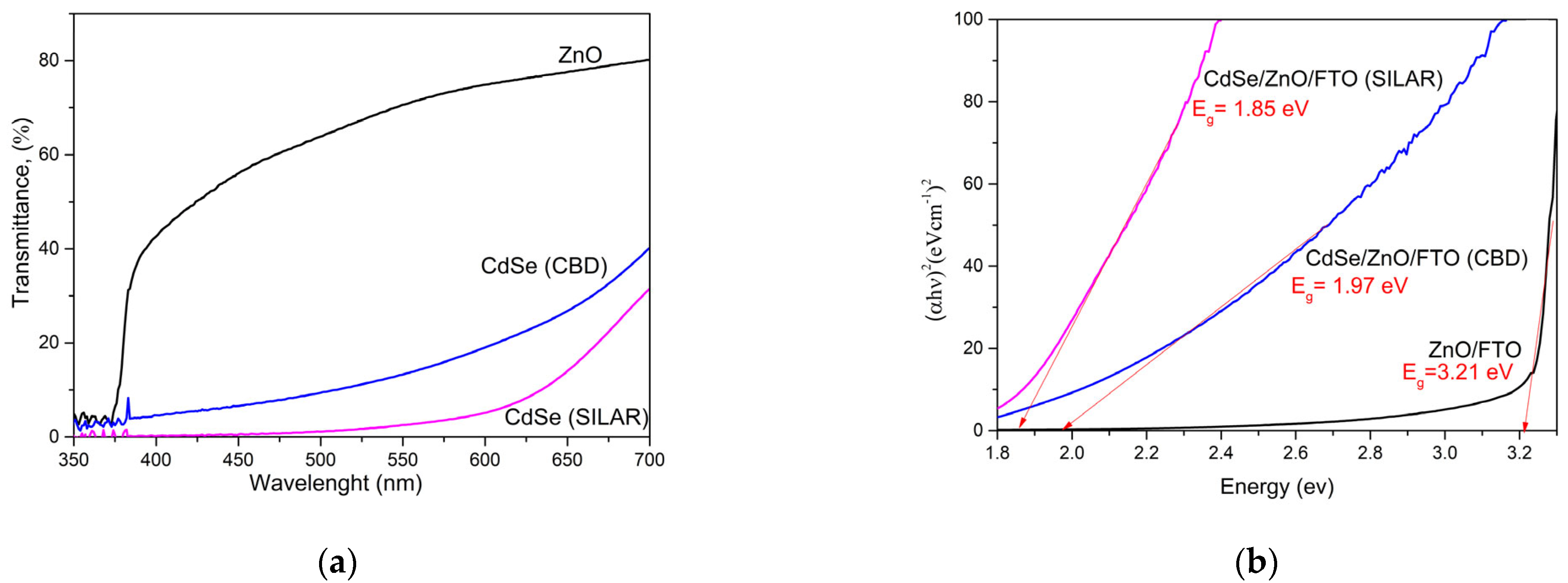
3.4. Optical Analysis

To investigate the optical properties, the UV–vis absorption spectra of the ZnO and CdSe/ZnO composites prepared on the FTO substrate were measured. As can be seen in Figure 2, the FTO with a thin layer of ZnO was white, while the color of the thin film of CdSe/ZnO changed to dark brown. Meanwhile, ZnO showed strong absorption in the ultraviolet region with a spectral wavelength of around 380 nm (Figure 6a). On the contrary, pure ZnO exhibited negligible absorption in the visible region, beyond 400 nm. However, the incorporation of a CdSe/ZnO composite resulted in a noticeable broadening of the absorption spectrum that extended into the visible range. Subsequent to the deposition of a CdSe layer on ZnO, a shift in the absorption peak toward the visible region was observed. This shift can be attributed to the effects of quantum confinement on the CdSe/ZnO semiconductor. This observation signifies that the CdSe/ZnO semiconductor had an optimal band gap, thus facilitating visible light activation and improving photocatalytic efficiency [33]. The absorption intensity of CdSe was notably higher than that of ZnO, indicating that the thin film structure consisted of a greater proportion of CdSe relative to that of ZnO. The experimental findings demonstrate that CdSe/ZnO composites exhibit remarkable efficacy in capturing the visible portion of solar radiation. Consequently, CdSe/ZnO heterostructures have the potential to function as efficient photocatalysts under visible light.
As demonstrated in Figure 6b, the band gap value calculated for ZnO was 3.21 eV, which corresponds to the value reported in the literature [33,38]. This band gap value is too large for visible light absorption; however, it was significantly reduced when ZnO was coated with a CdSe layer. The band gap calculated for CdSe/ZnO, formed at different deposition methods, varied from Eg = 1.85 eV (SILAR) to Eg = 1.97 eV (CBD) (Figure 6b). It is noteworthy that these values exhibit a substantial shift compared to those observed for bulk crystalline CdSe, which has an Eg of 1.73 eV [9].
The observation of an enlarged band gap energy is indicative of the impact of quantum size, attributable to the diminutive crystallite size [35]. This outcome is attributable to the interfacial combination and the matched band edges between ZnO and CdSe. It has been demonstrated that approximately 80% of light can be absorbed by a CdSe layer with a thickness of less than 40 nm, underscoring the potential of CdSe as an absorber. This phenomenon is believed to be attributable to defect states that accumulate at the periphery of the band. However, alternative explanations, such as strain and interactions between neighboring quantum confined nanocrystals, have also been proposed [25,34,39,40].
The results demonstrate that the CdSe layer enhanced the photoabsorption capacity of ZnO in the visible region. The observed shift in band gap energy after CdSe deposition is consistent with the existing literature [1,23,35]. However, a direct comparison of the exact band gap values is impractical due to their sensitivity to specific synthesis conditions, including precursor concentrations, immersion time in each solution, and precycle sample treatments (e.g., drying, annealing).

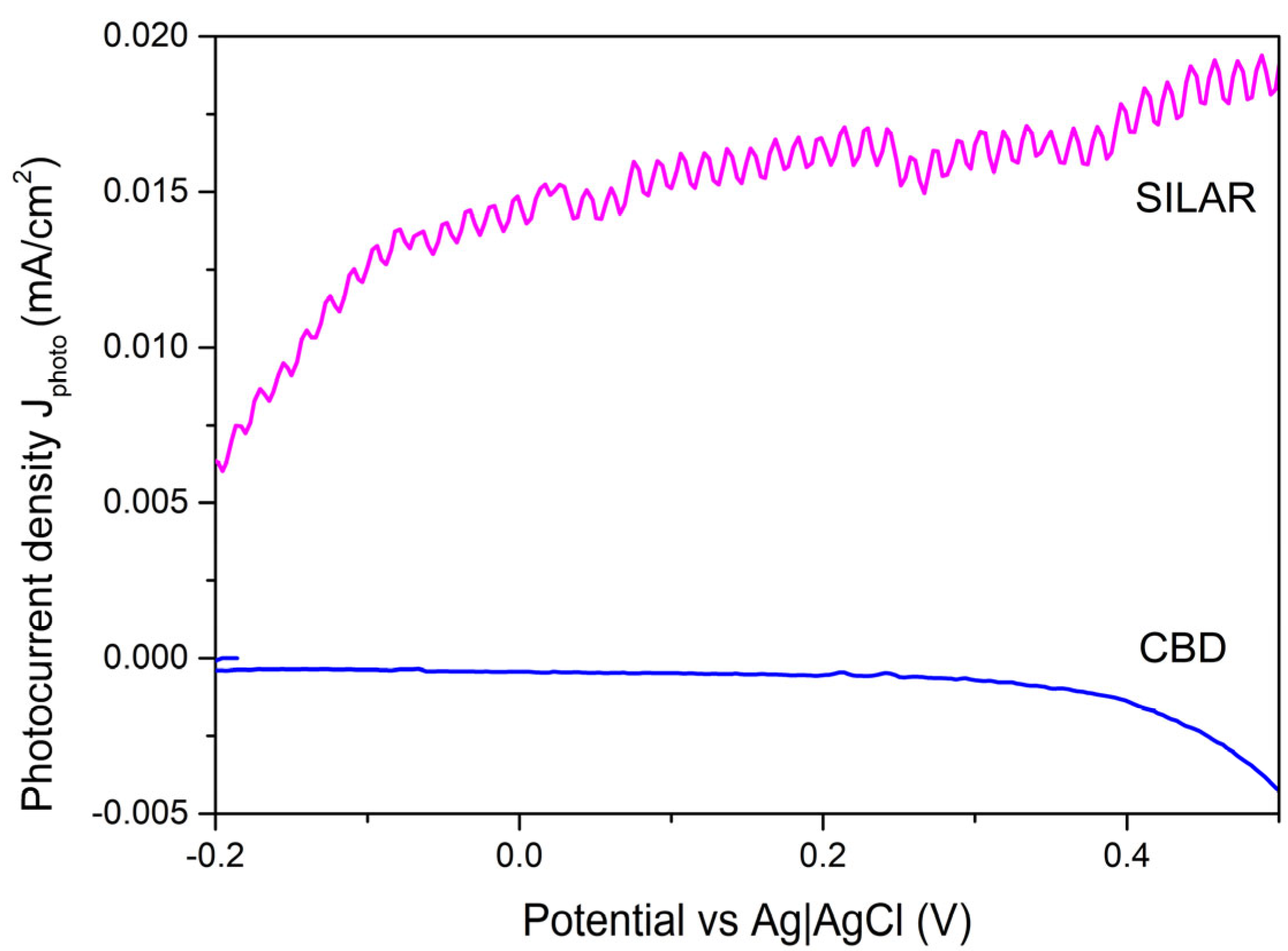
3.5. Electrochemical Analysis

A linear sweep voltammetry study of the thin film CdSe/ZnO is illustrated in Figure 7 and Table 4. Figure 7 shows the variation of the photocurrent density on the potential in CdSe/ZnO thin films formed by two distinct methods. The samples prepared by the SILAR method exhibited the highest photocurrent catalytic activity, with positive photocurrent values indicative of photogenerated charge carriers moving in the desired directions within the energy band diagram. On the contrary, samples prepared by the CBD method displayed negative photocurrent values, suggesting that ZnO conduction is greater than CdSe in the energy band alignment, potentially causing electrons to flow from CdSe to ZnO, resulting in negative photocurrent values.
This analysis indicates that the SILAR method for forming CdSe/ZnO layers on FTO results in materials with high photocurrent values, rendering them suitable for integration and use in photoelectrochemical applications.

4. Conclusions

In this study, we successfully fabricated CdSe/ZnO thin films on FTO substrates using low-temperature chemical bath deposition and SILAR methods. Each method has unique advantages for thin film fabrication, and both are low-cost and suitable for large-area production. The CdSe/ZnO thin films were thoroughly characterized by different standard techniques. The XRD patterns revealed that the crystalline phases of the CdSe/ZnO thin films consisted of hexagonal wurtzite ZnO and cubic CdSe using both deposition methods. The crystallite size of ZnO and CdSe/ZnO was found to be ~44 nm and ~10 nm, respectively. Analysis utilizing SEM and AFM revealed that the films prepared using the CBD method exhibited enhanced density, superior crystallinity, greater uniformity and homogeneity, and more compact structure in comparison to the CdSe/ZnO films obtained by depositing CdSe on the surface of ZnO/FTO using the SILAR method. The UV–vis spectroscopy investigation yielded a direct band gap value of 3.2 eV for the ZnO layer on the FTO. The band gap of CdSe/ZnO, formed by different deposition methods, ranged from Eg = 1.85 eV (SILAR) to Eg = 1.97 eV (CBD). Elemental analysis confirmed the formation of a CdSe/ZnO heterostructure with a CdSe stoichiometric ratio of approximately 1:1, verifying the successful deposition of stoichiometric CdSe on ZnO. The CdSe/ZnO thin film exhibited optimal photocatalytic efficiency when formed using the SILAR method. Consequently, the CdSe/ZnO thin films exhibited superior optical, morphological, and electrical properties, along with the highest photocurrent value, when the CdSe layers were formed using the SILAR method. It is evident that employing diverse techniques for thin film growth will yield various efficiencies for photovoltaic devices.

Author Contributions

Conceptualization, N.P. and G.J.; methodology, G.J. and N.P.; validation, N.P. and G.J.; formal analysis, N.P., G.J. and E.U.; investigation, G.J. and. E.U; data curation, G.J. and N.P.; writing—original draft preparation, G.J. and N.P.; writing—review and editing, G.J., N.P., E.P. and E.U.; visualization, G.J., N.P. and E.U.; supervision, N.P. and E.P. All authors have read and agreed to the published version of the manuscript.

Funding

This research received no external funding.

Institutional Review Board Statement

Not applicable.

Informed Consent Statement

Not applicable.

Data Availability Statement

Data will be made available on request.

Conflicts of Interest

The authors declare no conflicts of interest.

References

  1. Oloruntoba, S.O.; Zainal, Z.; Sulaiman, Y.; Zawawi, R.M.; Tan, H.J. Annealing Temperature Effect on the Characteristics of CdSe/ZnO Nanorod Heterostructures Fabricated by SILAR-Technique for Improved Photoelectrochemical Cell Performance. Opt. Mater. 2025, 160, 116636. [Google Scholar] [CrossRef]
  2. Jiang, C.; Moniz, S.J.A.; Wang, A.; Zhang, T.; Tang, J. Photoelectrochemical Devices for Solar Water Splitting—Materials and Challenges. Chem. Soc. Rev. 2017, 46, 4645–4660. [Google Scholar] [CrossRef] [PubMed]
  3. Liu, J.; Luo, Z.; Mao, X.; Dong, Y.; Peng, L.; Sun-Waterhouse, D.; Kennedy, J.V.; Waterhouse, G.I.N.; Liu, J.; Luo, Z.; et al. Recent Advances in Self-Supported Semiconductor Heterojunction Nanoarrays as Efficient Photoanodes for Photoelectrochemical Water Splitting. Small 2022, 18, 2204553. [Google Scholar] [CrossRef]
  4. Baviskar, P.K.; Dubal, D.P.; Majumder, S.; Ennaoui, A.; Sankapal, B.R. “Basic Idea, Advance Approach”: Efficiency Boost by Sensitization of Blended Dye on Chemically Deposited ZnO Films. J. Photochem. Photobiol. A Chem. 2016, 318, 135–141. [Google Scholar] [CrossRef]
  5. Chen, J.; Wu, J.; Lei, W.; Song, J.L.; Deng, W.Q.; Sun, X.W. Co-Sensitized Quantum Dot Solar Cell Based on ZnO Nanowire. Appl. Surf. Sci. 2010, 256, 7438–7441. [Google Scholar] [CrossRef]
  6. Qiu, X.; Que, W.; Yin, X.; Zhang, J.; Chen, J. ZnO/CdS/CdSe Core/Double Shell Nanorod Arrays Derived by a Successive Ionic Layer Adsorption and Reaction Process for Quantum Dot-Sensitized Solar Cells. Semicond. Sci. Technol. 2011, 26, 095028. [Google Scholar] [CrossRef]
  7. Nikam, P.R.; Baviskar, P.K.; Majumder, S.; Sali, J.V.; Sankapal, B.R. SILAR Controlled CdSe Nanoparticles Sensitized ZnO Nanorods Photoanode for Solar Cell Application: Electrolyte Effect. J. Colloid Interface Sci. 2018, 524, 148–155. [Google Scholar] [CrossRef]
  8. Güell, F.; Galdámez-Martínez, A.; Martínez-Alanis, P.R.; Catto, A.C.; da Silva, L.F.; Mastelaro, V.R.; Santana, G.; Dutt, A. ZnO-Based Nanomaterials Approach for Photocatalytic and Sensing Applications: Recent Progress and Trends. Mater. Adv. 2023, 4, 3685–3707. [Google Scholar] [CrossRef]
  9. Li, K.; Lin, X.; Song, B.; Kondrotas, R.; Wang, C.; Lu, Y.; Yang, X.; Chen, C.; Tang, J. Rapid Thermal Evaporation for Cadmium Selenide Thin-Film Solar Cells. Front. Optoelectron. 2021, 14, 482–490. [Google Scholar] [CrossRef]
  10. Mahato, S.; Shakti, N.; Kar, A.K. Annealing Temperature Dependent Structural and Optical Properties of Electrodeposited CdSe Thin Films. Mater. Sci. Semicond. Process. 2015, 39, 742–747. [Google Scholar] [CrossRef]
  11. Bera, S.; Singh, S.B.; Ray, S.K. Green Route Synthesis of High Quality CdSe Quantum Dots for Applications in Light Emitting Devices. J. Solid State Chem. 2012, 189, 75–79. [Google Scholar] [CrossRef]
  12. Mahato, S.; Kar, A.K. The Effect of Annealing on Structural, Optical and Photosensitive Properties of Electrodeposited Cadmium Selenide Thin Films. J. Sci. Adv. Mater. Devices 2017, 2, 165–171. [Google Scholar] [CrossRef]
  13. Inbanathan, F.P.N.; Kumar, P.; Dasari, K.; Katiyar, R.S.; Chen, J.; Jadwisienczak, W.M. Ellipsometry Study of CdSe Thin Films Deposited by PLD on ITO Coated Glass Substrates. Materials 2021, 14, 3307. [Google Scholar] [CrossRef] [PubMed]
  14. Parajuli, D.; Kc, D.; Khattri, K.B.; Adhikari, D.R.; Gaib, R.A.; Shah, D.K. Numerical Assessment of Optoelectrical Properties of ZnSe–CdSe Solar Cell-Based with ZnO Antireflection Coating Layer. Sci. Rep. 2023, 13, 12193. [Google Scholar] [CrossRef]
  15. Xie, Y.; Madel, M.; Li, Y.; Jie, W.; Neuschl, B.; Feneberg, M.; Thonke, K. Polarity-Controlled Ultraviolet/Visible Light ZnO Nanorods/p-Si Photodetector. J. Appl. Phys. 2012, 112, 123111. [Google Scholar] [CrossRef]
  16. Zhu, H.; Shan, C.X.; Yao, B.; Li, B.H.; Zhang, J.Y.; Zhao, D.X.; Shen, D.Z.; Fan, X.W. High Spectrum Selectivity Ultraviolet Photodetector Fabricated from an N-ZnO/p-GaN Heterojunction. J. Phys. Chem. C 2008, 112, 20546–20548. [Google Scholar] [CrossRef]
  17. Leschkies, K.S.; Divakar, R.; Basu, J.; Enache-Pommer, E.; Boercker, J.E.; Carter, C.B.; Kortshagen, U.R.; Norris, D.J.; Aydil, E.S. Photosensitization of ZnO Nanowires with CdSe Quantum Dots for Photovoltaic Devices. Nano Lett. 2007, 7, 1793–1798. [Google Scholar] [CrossRef]
  18. Haque, A.; Zechel, F.; Vretenár, V.; Roy, M.; Sýkora, M. Type-II CdSe/ZnO Core/Shell Nanorods: Nanoheterostructures with A Tunable Dual Emission in Visible and Near-Infrared Spectral Ranges. Adv. Funct. Mater. 2024, 34, 2305296. [Google Scholar] [CrossRef]
  19. Jain, S.; Sharma, S.N.; Kumar, M. Synthesis and Properties of CdSe Quantum Dot Sensitized ZnO Nanocomposites. Phys. E Low-Dimens. Syst. Nanostruct. 2011, 44, 555–564. [Google Scholar] [CrossRef]
  20. Ramírez-Amador, R.; Flores-Carrasco, G.; Alcántara-Iniesta, S.; Rodríguez González, J.; García-Teniza, O.; Mercado-Agular, E.; Vásquez-Ortiz, A.B. Structural, Morphological, Optical, and Electrical Characterization of Fluorine Doped Tin Oxide (FTO) Thin Films Synthesized by PSP. Solid State Phenom. 2019, 286, 64–71. [Google Scholar]
  21. Sudhagar, P.; Chandramohan, S.; Kumar, R.S.; Sathyamoorthy, R.; Hong, C.H.; Kang, Y.S. Fabrication and Charge-Transfer Characteristics of CdS QDs Sensitized Vertically Grown Flower-like ZnO Solar Cells with CdSe Cosensitizers. Phys. Status Solidi (A) Appl. Mater. Sci. 2011, 208, 474–479. [Google Scholar] [CrossRef]
  22. Chen, Y.; Wei, L.; Zhang, G.; Jiao, J. Open Structure ZnO/CdSe Core/Shell Nanoneedle Arrays for Solar Cells. Nanoscale Res. Lett. 2012, 7, 1–6. [Google Scholar] [CrossRef]
  23. Zarębska, K.; Łęcki, T.; Skompska, M. Synthesis of CdSe on FTO-Supported ZnO Nanorods by SILAR and Electrochemical Methods and Comparison of Photoelectrochemical Properties of FTO/ZnO/CdSe Systems in Aqueous S2−/Sn2− Electrolyte. J. Electroanal. Chem. 2018, 819, 459–468. [Google Scholar] [CrossRef]
  24. Pan, S.; Ebrahim, S.; Soliman, M.; Qiao, Q. Seed-Mediated Direct Growth of CdSe Nanoclusters on Substrates. J. Nanoparticle Res. 2013, 15, 1420. [Google Scholar] [CrossRef]
  25. Majidi, H.; Baxter, J.B. Electrodeposition of CdSe Coatings on ZnO Nanowire Arrays for Extremely Thin Absorber Solar Cells. Electrochim. Acta 2011, 56, 2703–2711. [Google Scholar] [CrossRef]
  26. Bragg, W.H.; Bragg, W.L. The Reflection of X-Rays by Crystals. Proc. R. Soc. Lond. Ser. A Contain. Pap. A Math. Phys. Character 1913, 88, 428–438. [Google Scholar] [CrossRef]
  27. Patterson, A.L. The Scherrer Formula for X-Ray Particle Size Determination. Phys. Rev. 1939, 56, 978. [Google Scholar] [CrossRef]
  28. Nath, D.; Singh, F.; Das, R. X-Ray Diffraction Analysis by Williamson-Hall, Halder-Wagner and Size-Strain Plot Methods of CdSe Nanoparticles- a Comparative Study. Mater. Chem. Phys. 2020, 239, 122021. [Google Scholar] [CrossRef]
  29. Tauc, J.; Grigorovici, R.; Vancu, A. Optical Properties and Electronic Structure of Amorphous Germanium. Phys. Status Solidi (b) 1966, 15, 627–637. [Google Scholar] [CrossRef]
  30. Makuła, P.; Pacia, M.; Macyk, W. How To Correctly Determine the Band Gap Energy of Modified Semiconductor Photocatalysts Based on UV-Vis Spectra. J. Phys. Chem. Lett. 2018, 9, 6814–6817. [Google Scholar] [CrossRef]
  31. El-Naggar, M.E.; Hassabo, A.G.; Mohamed, A.L.; Shaheen, T.I. Surface Modification of SiO2 Coated ZnO Nanoparticles for Multifunctional Cotton Fabrics. J. Colloid Interface Sci. 2017, 498, 413–422. [Google Scholar] [CrossRef]
  32. Nishinaka, H.; Kamada, Y.; Kameyama, N.; Fujita, S. Epitaxial ZnO Thin Films on A-Plane Sapphire Substrates Grown by Ultrasonic Spray-Assisted Mist Chemical Vapor Deposition. Jpn. J. Appl. Phys. 2009, 48, 121103. [Google Scholar] [CrossRef]
  33. Chen, X.; Li, J. Assembly and Photocatalytic Degradation Activity of Spherical ZnO/CdSe Heterostructures on Flexible Carbon Cloth Substrates. Nanomaterials 2022, 12, 1898. [Google Scholar] [CrossRef] [PubMed]
  34. Aldeek, F.; Mustin, C.; Balan, L.; Medjahdi, G.; Roques-Carmes, T.; Arnoux, P.; Schneider, R. Enhanced Photostability from CdSe(S)/ZnO Core/Shell Quantum Dots and Their Use in Biolabeling. Eur. J. Inorg. Chem. 2011, 2011, 794–801. [Google Scholar] [CrossRef]
  35. Raghunath Sankapal, B.; Zhang, J.; Yoshida, T.; Minoura, H. Electrochemical Fabrication of Nanoporous ZnO/Q-CdSe Photovoltaic Device. Trans. Mater. Res. Soc. Japan 2006, 31, 429–432. [Google Scholar]
  36. Qian, L.; Yang, J.; Zhou, R.; Tang, A.; Zheng, Y.; Tseng, T.K.; Bera, D.; Xue, J.; Holloway, P.H. Hybrid Polymer-CdSe Solar Cells with a ZnO Nanoparticle Buffer Layer for Improved Efficiency and Lifetime. J. Mater. Chem. 2011, 21, 3814–3817. [Google Scholar] [CrossRef]
  37. Barceló, I.; Lana-Villarreal, T.; Gómez, R. Efficient Sensitization of ZnO Nanoporous Films with CdSe QDs Grown by Successive Ionic Layer Adsorption and Reaction (SILAR). J. Photochem. Photobiol. A Chem. 2011, 220, 47–53. [Google Scholar] [CrossRef]
  38. Srikant, V.; Clarke, D.R. On the Optical Band Gap of Zinc Oxide. J. Appl. Phys. 1998, 83, 5447–5451. [Google Scholar] [CrossRef]
  39. Hodes, G.; Grunbaum, E.; Feldman, Y.; Bastide, S.; Lévy-Clément, C. Variable Optical Properties and Effective Porosity of CdSe Nanocrystalline Films Electrodeposited from Selenosulfate Solutions. J. Electrochem. Soc. 2005, 152, G917. [Google Scholar] [CrossRef]
  40. Wu, Y.; Xu, F.; Guo, D.; Gao, Z.; Wu, D.; Jiang, K. Synthesis of ZnO/CdSe Hierarchical Heterostructure with Improved Visible Photocatalytic Efficiency. Appl. Surf. Sci. 2013, 274, 39–44. [Google Scholar] [CrossRef]
Figure 1. Band diagram of the CdSe-ZnO interface.
Coatings 15 00415 g001
Figure 2. Steps of preparation of CdSe/ZnO thin films on FTO.
Coatings 15 00415 g002
Figure 3. X-ray diffraction patterns of bare FTO (a, 1 curve), ZnO/FTO (a, 2 curve), CdSe/ZnO/FTO (SILAR) (a, 3 curve and b), and CdSe/ZnO/FTO(CBD) (a, 4 curve and c).
Coatings 15 00415 g003
Figure 4. SEM images of pristine FTO (a), ZnO/FTO (b), and thin films of CdSe obtained by SILAR (c) and CBD (d).
Coatings 15 00415 g004aCoatings 15 00415 g004b
Figure 5. 3D AFM images (top) and profiles (bottom) of the pristine surface of FTO (a), ZnO/FTO (b), and thin films of CdSe obtained by SILAR (c) and CBD (d).
Coatings 15 00415 g005aCoatings 15 00415 g005b
Figure 6. UV–vis transmittance spectra of ZnO and CdSe thin films obtained on ZnO/FTO surfaces by different methods (a); a plot of (αhν)2 versus photon energy (b).
Coatings 15 00415 g006
Figure 7. Dependence of photocurrent variation (under illumination) on the potential for CdSe thin films deposited on ZnO/FTO surfaces using different methods.
Coatings 15 00415 g007
Table 1. XRD data of CdSe/ZnO and comparison with JCPDS data of observed d values with standard d values.
Peaks Assigned to MaterialsAnalysis ResultsJCPDS Data
2θd, Ǻd, ǺMiller Indexes (hkl)PDF No.Crystalline
Phase
FTO26.783.333.35(110)71-0652Cassiterite SnO2
tetragonal
33.962.642.64(101)
37.982.372.37(200)
51.751.771.76(211)
61.991.501.49(310)
65.821.421.42(301)
ZnO31.942.802.81(100)36-1451Wurtzite ZnO
hexagonal
34.612.592.60(002)
36.422.462.48(101)
47.941.891.91(102)
57.051.611.62(110)
63.291.471.47(103)
68.371.371.38(112)
CdSe25.373.513.37(111)19-191CdSe cubic
42.032.152.02(220)
49.761.831.68(311)
Table 2. Morphology parameters of CdSe/ZnO on the FTO surface.
ParametersFTOZnO/FTOCdSe/ZnO/FTOCdSe/ZnO/FTO
---SILAR CBD
Average roughness, Ra, nm12.6111.4958.1950.64
RMS roughness, Rq, nm15.8514.4978.6763.95
Maximum surface roughness, Rt, nm143.30124.801012.00531.40
Table 3. Results of elemental EDX analysis of CdSe/ZnO thin films obtained by using different CdSe layer formation methods.
CdSe Layer Formation Method Zn, at%O, at%Cd, at%Se, at%Cd/Se
SILAR13.9338.6910.449.001.16
CBD0.0524.5813.2612.131.09
Table 4. LSV results of CdSe/ZnO thin films at a potential value of 0.5 V.
CdSe Forming MethodSample Surface Area A, cm2Current Density juv Value Achieved Using UV Radiation, mA/cm2Current Density jdark Value Achieved in the Dark, mA/cm2juv/jdarkPhotocurrent jphoto, mA/cm2
SILAR1.950.02320.00386.0630.0938
CBD1.050.00110.00550.2−0.044
Disclaimer/Publisher’s Note: The statements, opinions and data contained in all publications are solely those of the individual author(s) and contributor(s) and not of MDPI and/or the editor(s). MDPI and/or the editor(s) disclaim responsibility for any injury to people or property resulting from any ideas, methods, instructions or products referred to in the content.

