
Research on Titanium Ion Etching Pretreatment Process on Cemented Carbide Before DLC Film Deposition


Abstract
:
1. Introduction
2. Experiment Details
2.1. Etching Pre-Treatment and DLC Films Deposition
2.2. Characteristics Measurement
3. Results and Discussion
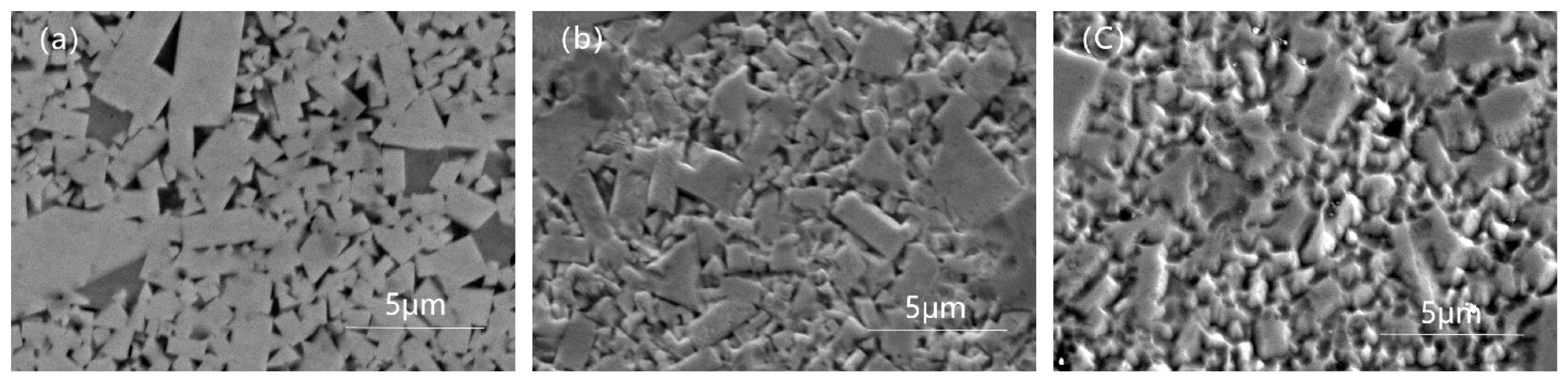
3.1. Surface Characteristics Changed by Etching Parameters
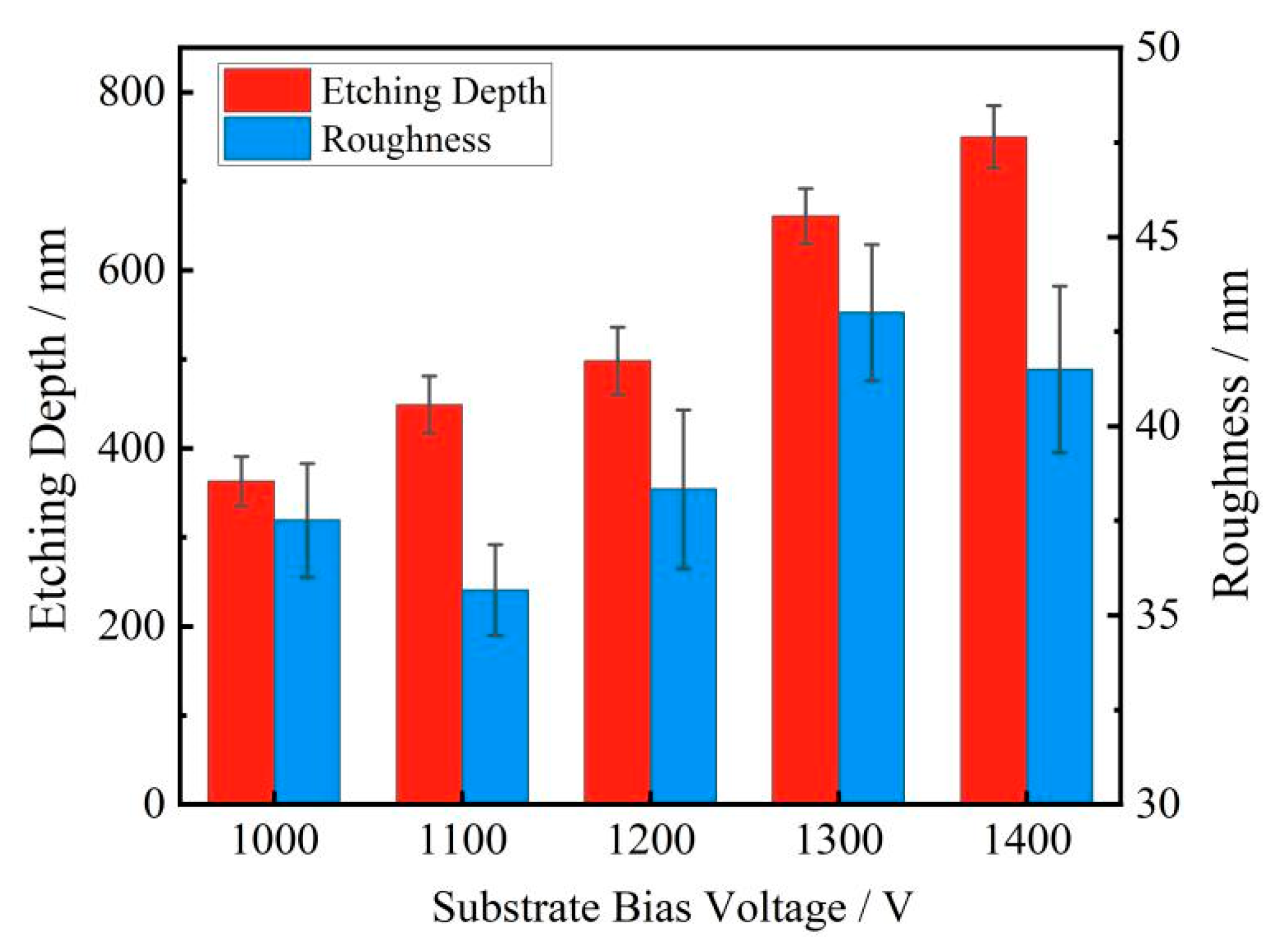
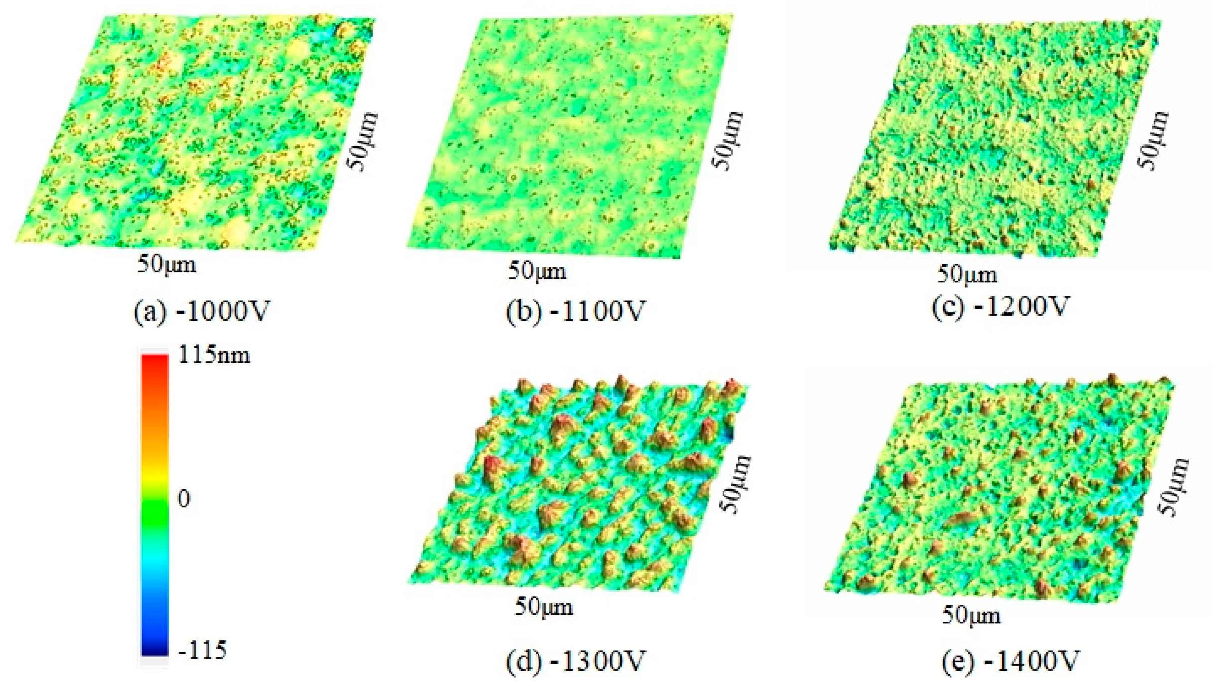
3.1.1. Substrate Bias Voltage
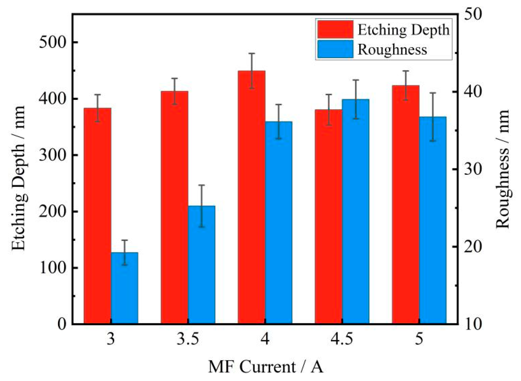
3.1.2. MF Current
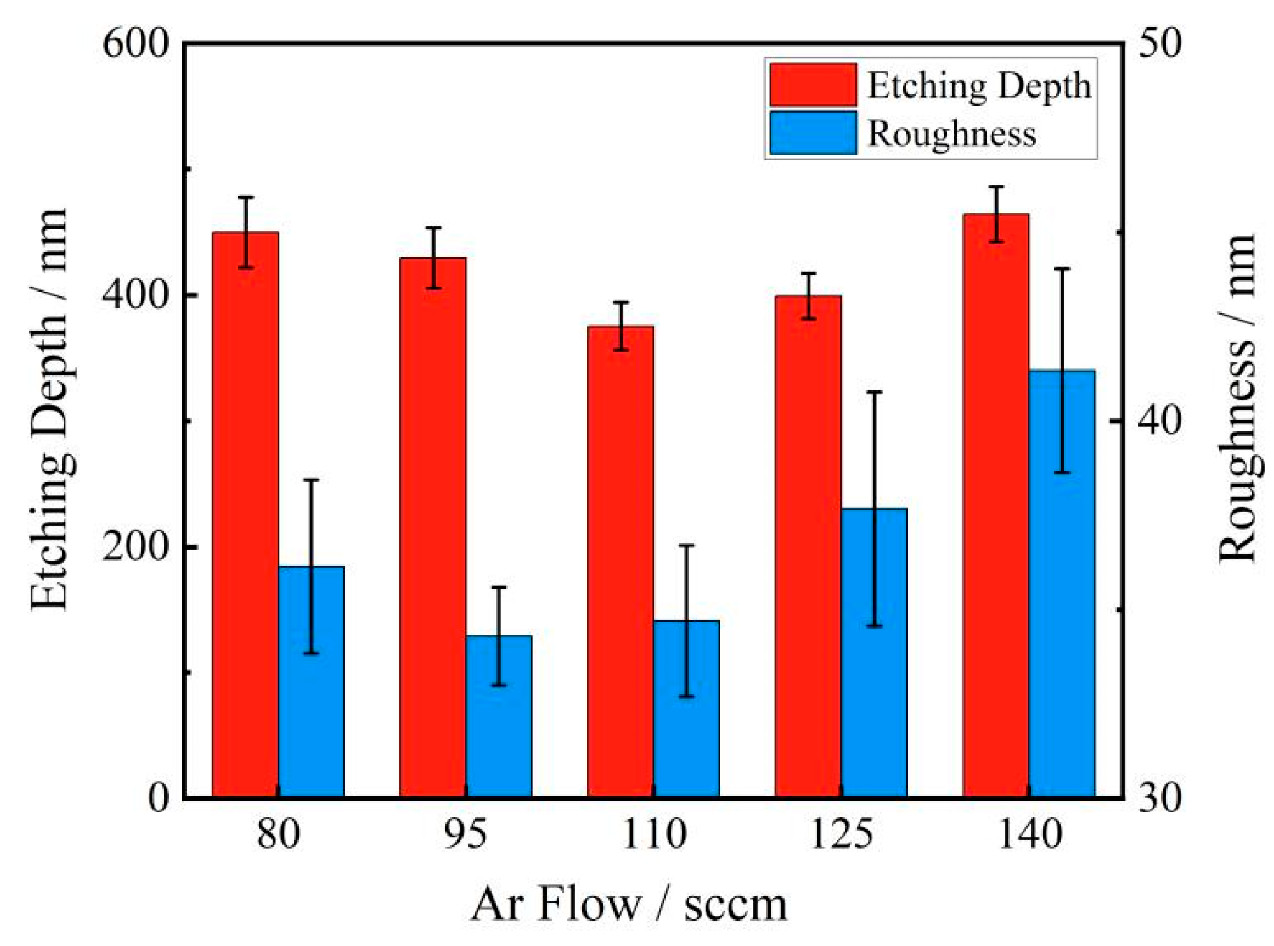
3.1.3. Ar Flow
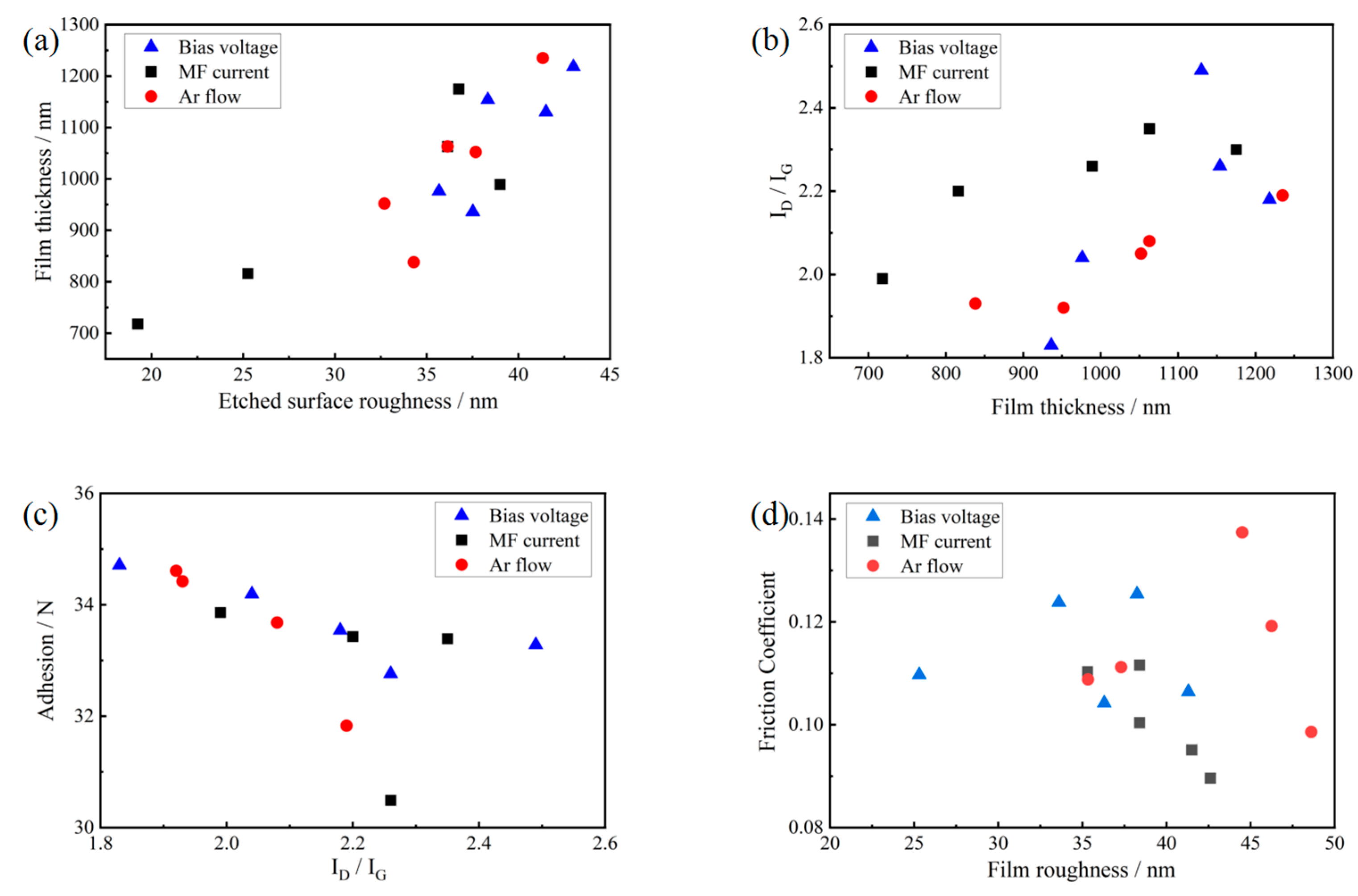
3.2. Key Factors of Etched Surface Influencing DLC Properties
3.2.1. Surface Roughness
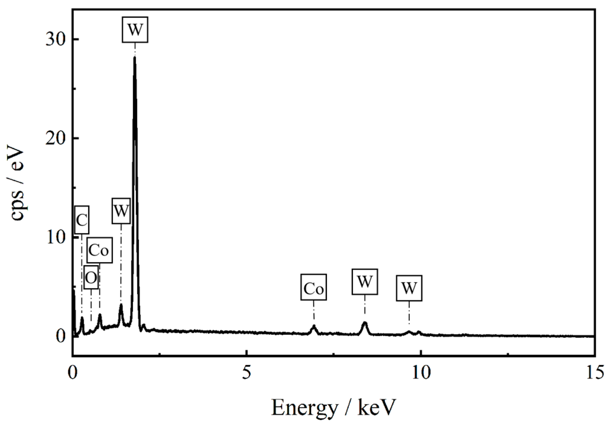
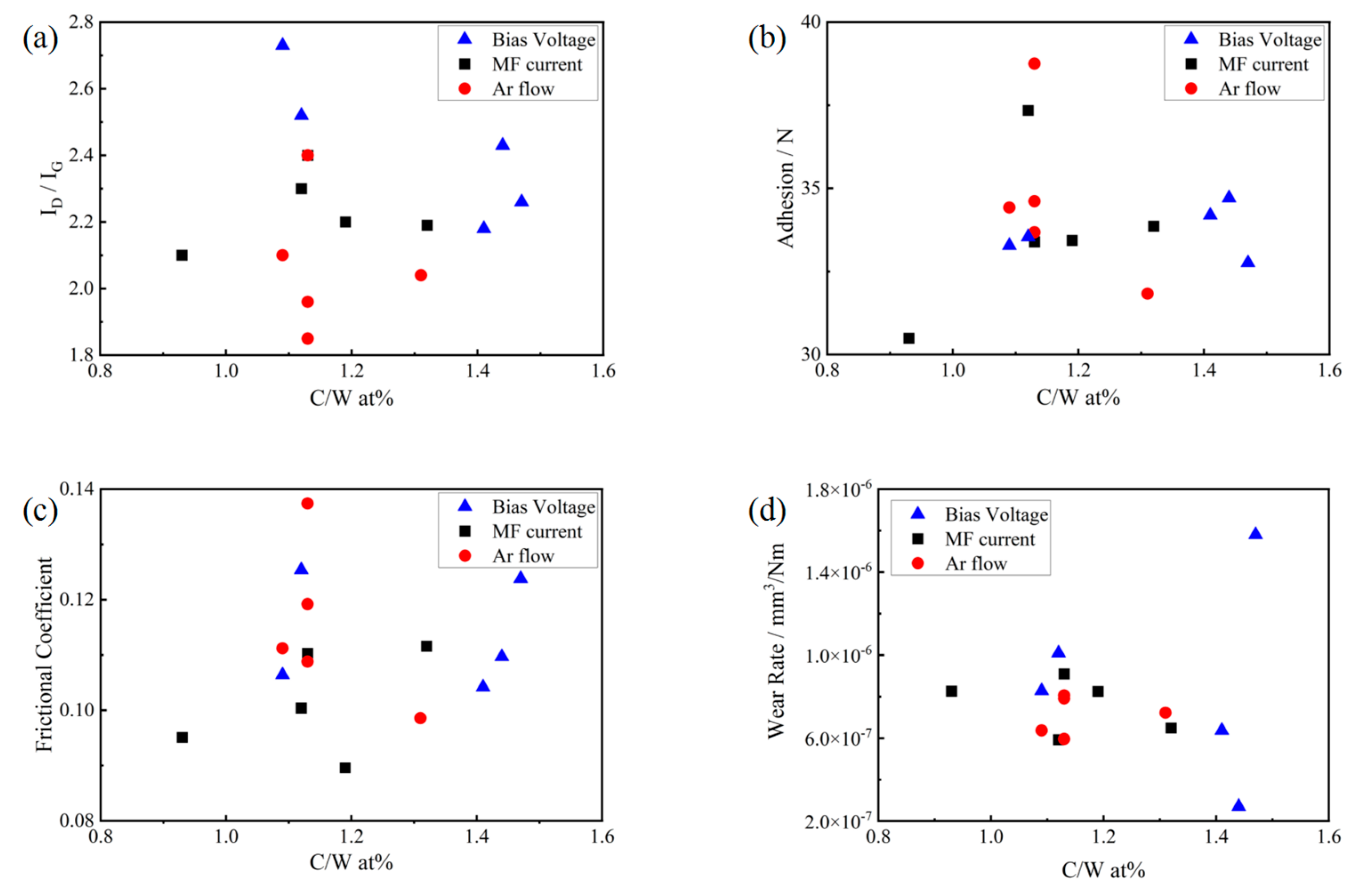
3.2.2. C/W Ratio
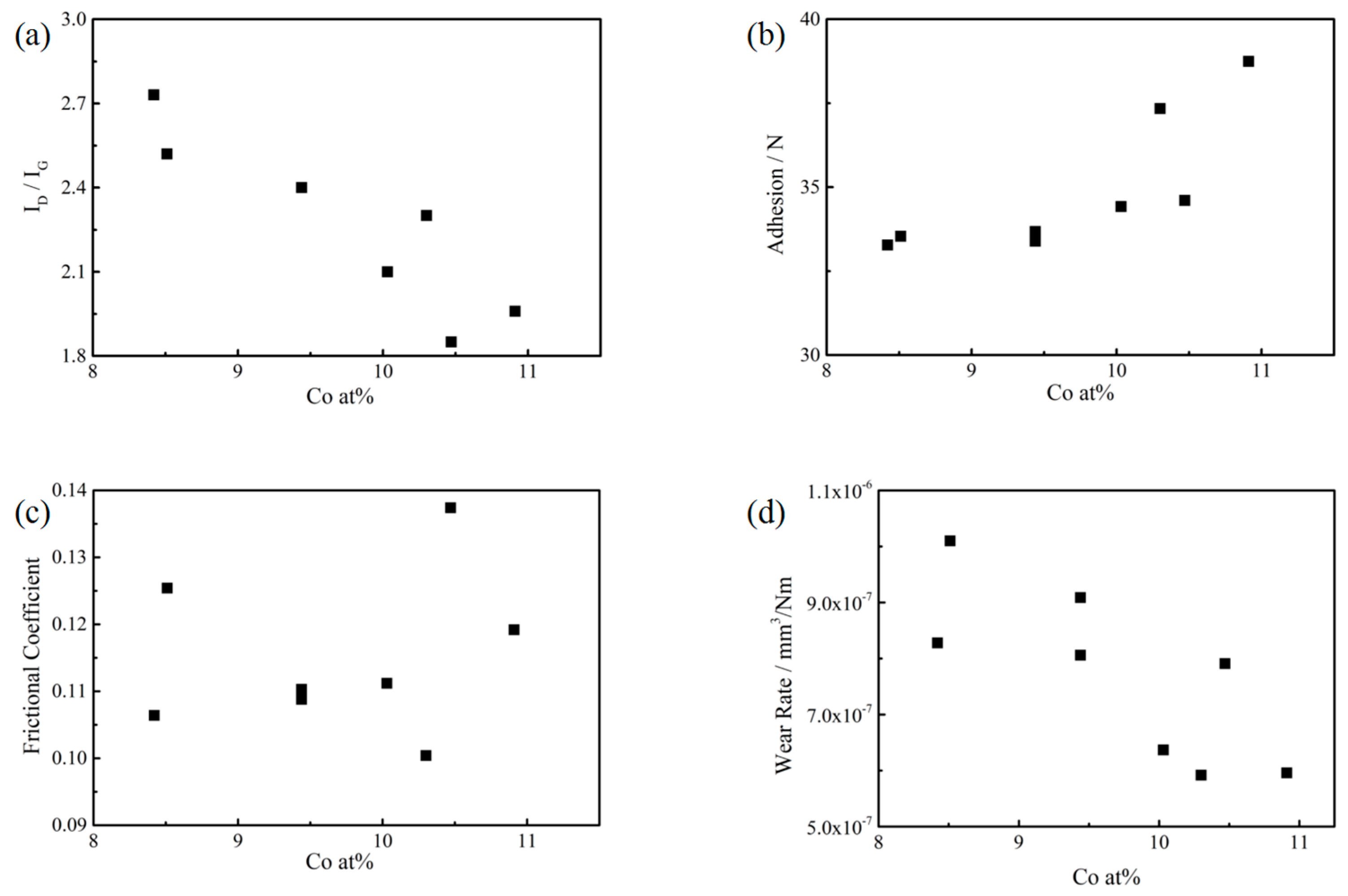
3.2.3. Co Content
4. Conclusions
Author Contributions
Funding
Data Availability Statement
Conflicts of Interest
References
- Su, Y.; Huang, W.; Cai, L.; Gong, X.; Zhang, T.; Hu, R.; Zhang, P.; Ruan, H. Microstructural evolution and tribology of Mo-doped diamond like carbon nanocomposite film. Tribol. Int. 2022, 174, 107774. [Google Scholar]
- Peng, Y.; Peng, J.; Wang, Z.; Xiao, Y.; Qiu, X. Diamond-like Carbon Coatings in the Biomedical Field: Properties, Applications and Future Development. Coatings 2022, 12, 1088. [Google Scholar] [CrossRef]
- Wei, C.; Pan, W.; Hung, M. The effects of substrate roughness and associated surface properties on the biocompatibility of diamond-like carbon films. Surf. Coat. Technol. 2013, 224, 8–17. [Google Scholar]
- Tzeng, S.; Wu, Y.; Hsu, J. The effects of plasma pre-treatment and post-treatment on diamond-like carbon films synthesized by RF plasma enhanced chemical vapor deposition. Vacuum 2008, 83, 618–621. [Google Scholar] [CrossRef]
- Khan, S.A.; Oliveira, J.; Ferreira, F.; Emami, N.; Ramalho, A. Surface Roughness Influence on Tribological Behavior of HiPIMS DLC Coatings. Tribol. Trans. 2023, 66, 565–575. [Google Scholar]
- Jacob, A.; Gangopadhyay, S.; Satapathy, A.; Mantry, S.; Jha, B.B. Influences of micro-blasting as surface treatment technique on properties and performance of AlTiN coated tools. J. Manuf. Process. 2017, 29, 407–418. [Google Scholar]
- Ozeki, K.; Masuzawa, T.; Hirakuri, K.K. The wear properties and adhesion strength of the diamond-like carbon film coated on SUS, Ti and Ni-Ti with plasma pre-treatment. Biomed. Mater. Eng. 2010, 20, 21–35. [Google Scholar]
- Lee, J.A.; Lin, C.R.; Pan, P.C.; Liu, C.W.; Sun, A.Y. Dramatically enhanced mechanical properties of diamond-like carbon films on polymer substrate for flexible display devices via argon plasma pretreatment. Chem. Phys. 2020, 529, 110551. [Google Scholar]
- Nakao, S.; Kimura, T.; Suyama, T.; Azuma, K. Conductive diamond-like carbon films prepared by high power pulsed magnetron sputtering with bipolar type plasma based ion implantation system. Diam. Relat. Mater. 2017, 77, 122–130. [Google Scholar] [CrossRef]
- Liu, L.; Wang, T.; Huang, J.; He, Z.; Yi, Y.; Du, K. Diamond-like carbon thin films with high density and low internal stress deposited by coupling DC/RF magnetron sputtering. Diam. Relat. Mater. 2016, 70, 151–158. [Google Scholar]
- Jiang, J.; Huang, H.; Wang, Q.; Zhu, W.; Hao, J.; Liu, W. Comparative study on structure and properties of titanium/silicon mono- and co-doped amorphous carbon films deposited by mid-frequency magnetron sputtering. Surf. Interface Anal. 2014, 46, 139–144. [Google Scholar] [CrossRef]
- Ponce, S.; Calderon, N.Z.; Ampuero, J.L.; La Rosa-Toro, A.; Talledo, A.; Gacitúa, W.; Pujada, B.R. Influence of the substrate bias on the stress in Ti-DLC films deposited by dc magnetron sputtering. Journal of physics. Conf. Ser. 2020, 1558, 12009. [Google Scholar] [CrossRef]
- Wu, Y.; Shi, B.; Liu, Y.; Wang, L.; Gao, J.; Shen, Y.; Wang, Y.; Ma, Y.; Yu, S. Design of Ta gradient layer to improve adhesion strength between Cu substrate and DLC film. Vacuum 2022, 203, 111221. [Google Scholar] [CrossRef]
- Kashyap, V.; Ramkumar, P. DLC coating over pre-oxidized and textured Ti6Al4V for superior adhesion and tribo-performance of hip implant. Surf. Coat. Technol. 2022, 440, 128492. [Google Scholar] [CrossRef]
- Wang, X.; Sui, X.; Zhang, S.; Yan, M.; Lu, Y.; Hao, J.; Liu, W. Impacts of the a-Si:H interlayer nanostructure on the adhesion of the thick DLC coatings prepared by PECVD. Appl. Surf. Sci. 2021, 565, 150539. [Google Scholar] [CrossRef]
- Kubart, T.; Fernandes, D.F.; Nyberg, T. On the description of metal ion return in reactive high power impulse magnetron sputtering. Surf. Coat. Technol. 2021, 418, 127234. [Google Scholar] [CrossRef]
- Guo, C.Q.; Li, H.Q.; Peng, Y.L.; Dai, M.J.; Lin, S.S.; Shi, Q.; Wei, C.B. Residual stress and tribological behavior of hydrogen-free Al-DLC films prepared by HiPIMS under different bias voltages. Surf. Coat. Technol. 2022, 445, 128713. [Google Scholar] [CrossRef]
- Nakao, S.; Yukimura, K.; Nakano, S.; Ogiso, H. DLC Coating by HiPIMS: The Influence of Substrate Bias Voltage. IEEE Trans. Plasma Sci. 2013, 41, 1819–1829. [Google Scholar] [CrossRef]
- Wasy, A.; Balakrishnan, G.; Lee, S.H.; Kim, J.K.; Kim, D.G.; Kim, T.G.; Song, J.I. Argon plasma treatment on metal substrates and effects on diamond-like carbon (DLC) coating properties. Cryst. Res. Technol. 2014, 49, 55–62. [Google Scholar] [CrossRef]
- Nguyen, T.; Ulrich, S.; Bsul, J.; Beauvais, S.; Burger, W.; Albers, A.; Stüber, M.; Ye, J. Influence of argon gas pressure and target power on magnetron plasma parameters. Diam. Relat. Mater. 2009, 18, 995–998. [Google Scholar] [CrossRef]
- Bonu, V.; Srinivas, G.; Kumar, V.P.; Joseph, A.; Narayana, C.; Barshilia, H.C. Temperature dependent erosion and Raman analyses of arc-deposited H free thick DLC coating on Cr/CrN coated plasma nitrided steel. Surf. Coat. Technol. 2022, 436, 128308. [Google Scholar] [CrossRef]
- Fu, Z.Q.; Wang, C.B.; Yue, W.; Peng, Z.J.; Lin, S.S.; Dai, M.J. Influence of Vacuum Cathodic Arc Etching on Structure and Properties of W-Doped DLC Films. Adv. Mater. Res. 2013, 787, 296–300. [Google Scholar] [CrossRef]
- Tillmann, W.; Dias, N.F.; Stangier, D.; Maus-Friedrichs, W.; Gustus, R.; Thomann, C.A.; Moldenhauer, H.; Debus, J. Improved adhesion of a-C and a-C:H films with a CrC interlayer on 16MnCr5 by HiPIMS-pretreatment. Surf. Coat. Technol. 2019, 375, 877–887. [Google Scholar]
- Santiago, J.A.; Fernández-Martínez, I.; Wennberg, A.; Molina-Aldareguia, J.M.; Castillo-Rodríguez, M.; Rojas, T.C.; Sánchez-López, J.C.; González, M.U.; García-Martín, J.M.; Li, H.; et al. Adhesion enhancement of DLC hard coatings by HiPIMS metal ion etching pretreatment. Surf. Coat. Technol. 2018, 349, 787–796. [Google Scholar]
- Peng, B.; Xu, Y.X.; Du, J.W.; Chen, L.; Kim, K.H.; Wang, Q. Influence of preliminary metal-ion etching on the topography and mechanical behavior of TiAlN coatings on cemented carbides. Surf. Coat. Technol. 2022, 432, 128040. [Google Scholar]
- Li, C.; Huang, L.; Yuan, J.; Zhou, D. The influence of Ti plasma etching pre-treatment on mechanical properties of DLC film on cemented carbide. Surf. Interface Anal. 2022, 54, 477–486. [Google Scholar] [CrossRef]
- Ward, L.; Junge, F.; Lampka, A.; Dobbertin, M.; Mewes, C.; Wienecke, M. The Effect of Bias Voltage and Gas Pressure on the Structure, Adhesion and Wear Behavior of Diamond Like Carbon (DLC) Coatings With Si Interlayers. Coatings 2014, 4, 214–230. [Google Scholar] [CrossRef]
- Liu, K.; Wang, Z.; Yin, Z.; Cao, L.; Yuan, J. Effect of Co content on microstructure and mechanical properties of ultrafine grained WC-Co cemented carbide sintered by spark plasma sintering. Ceram. Int. 2018, 44, 18711–18718. [Google Scholar]
- Zhang, D.; Shen, B.; Sun, F. Study on tribological behavior and cutting performance of CVD diamond and DLC films on Co-cemented tungsten carbide substrates. Appl. Surf. Sci. 2010, 256, 2479–2489. [Google Scholar]
- Li, B.; Zhang, Y.; Wu, Z.; Qin, Z.; Ji, H.; Liu, X.; Li, B.; Hu, W. Magnetic properties and corrosion resistance of Co-DLC nanocomposite films with different cobalt contents. Diam. Relat. Mater. 2021, 117, 108477. [Google Scholar]
- Tang, Y.; Li, Y.S.; Zhang, C.Z.; Wang, J.; Yang, Q.; Hirose, A. Synthesis of cobalt/diamond-like carbon thin films by biased target ion beam deposition. Diam. Relat. Mater. 2011, 20, 538–541. [Google Scholar]
- Guo, P.; Sun, L.; Li, X.; Xu, S.; Ke, P.; Wang, A. Structural properties and surface wettability of Cu-containing diamond-like carbon films prepared by a hybrid linear ion beam deposition technique. Thin Solid Films 2015, 584, 289–293. [Google Scholar]


| Substrate Bias Voltage/V | C at% | W at% | C/W Ratio | Co |
|---|---|---|---|---|
| 1000 | 54.56 | 37.89 | 1.44 | 7.55 |
| 1100 | 54.05 | 38.33 | 1.41 | 7.62 |
| 1200 | 54.82 | 37.30 | 1.47 | 7.88 |
| 1300 | 48.33 | 43.16 | 1.12 | 8.51 |
| 1400 | 47.76 | 43.82 | 1.09 | 8.42 |
| Mf Current/A | C at% | W at% | C/W Ratio | Co |
|---|---|---|---|---|
| 3 | 52.37 | 39.67 | 1.32 | 7.96 |
| 3.5 | 49.66 | 41.74 | 1.19 | 8.60 |
| 4 | 48.04 | 42.52 | 1.13 | 9.44 |
| 4.5 | 42.78 | 45.99 | 0.93 | 11.23 |
| 5 | 47.39 | 42.31 | 1.12 | 10.30 |
| Ar Flow/sccm | C at% | W at% | C/W Ratio | Co |
|---|---|---|---|---|
| 80 | 48.04 | 42.52 | 1.13 | 9.44 |
| 95 | 46.92 | 43.05 | 1.09 | 10.03 |
| 110 | 47.50 | 42.03 | 1.13 | 10.47 |
| 125 | 47.26 | 41.83 | 1.13 | 10.91 |
| 140 | 51.12 | 39.02 | 1.31 | 9.86 |
Disclaimer/Publisher’s Note: The statements, opinions and data contained in all publications are solely those of the individual author(s) and contributor(s) and not of MDPI and/or the editor(s). MDPI and/or the editor(s) disclaim responsibility for any injury to people or property resulting from any ideas, methods, instructions or products referred to in the content. |
© 2025 by the authors. Licensee MDPI, Basel, Switzerland. This article is an open access article distributed under the terms and conditions of the Creative Commons Attribution (CC BY) license (https://creativecommons.org/licenses/by/4.0/).
Share and Cite
Li, C.; Chen, J.; Huang, L. Research on Titanium Ion Etching Pretreatment Process on Cemented Carbide Before DLC Film Deposition. Coatings 2025, 15, 434. https://doi.org/10.3390/coatings15040434
Li C, Chen J, Huang L. Research on Titanium Ion Etching Pretreatment Process on Cemented Carbide Before DLC Film Deposition. Coatings. 2025; 15(4):434. https://doi.org/10.3390/coatings15040434
Chicago/Turabian StyleLi, Chao, Juan Chen, and Lei Huang. 2025. "Research on Titanium Ion Etching Pretreatment Process on Cemented Carbide Before DLC Film Deposition" Coatings 15, no. 4: 434. https://doi.org/10.3390/coatings15040434
APA StyleLi, C., Chen, J., & Huang, L. (2025). Research on Titanium Ion Etching Pretreatment Process on Cemented Carbide Before DLC Film Deposition. Coatings, 15(4), 434. https://doi.org/10.3390/coatings15040434