Abstract
With the increasing demand for alternatives to traditional indium tin oxide (ITO), copper nanowires (Cu NWs) have gained significant attention due to their excellent conductivity, cost-effectiveness, and ease of synthesis. However, challenges such as wire–wire contact resistance and oxidation susceptibility hinder their practical applications. This review discusses the development and challenges associated with Cu NW-based flexible transparent conductors (FTCs). Cu NWs are considered a promising alternative to traditional materials like ITO, thanks to their high electrical conductivity and low cost. This paper explores various synthesis methods for Cu NWs, including template-assisted synthesis, hydrazine reduction, and hydrothermal processes, while highlighting the advantages and limitations of each approach. The key challenges, such as contact resistance, oxidation, and the need for protective coatings, are also addressed. Several strategies to enhance the conductivity and stability of Cu NW-based FTCs are proposed, including thermal sintering, laser sintering, acid treatment, and photonic sintering. Additionally, protective coatings like noble metal core–shell layers, electroplated layers, and conductive polymers like PEDOT:PSS are discussed as effective solutions. The integration of graphene with Cu NWs is explored as a promising method to improve oxidation resistance and overall performance. The review concludes with an outlook on the future of Cu NWs in flexible electronics, emphasizing the need for scalable, cost-effective solutions to overcome current challenges and improve the practical application of Cu NW-based FTCs in advanced technologies such as displays, solar cells, and flexible electronics.
1. Introduction
Flexible transparent conductors (FTCs) are essential for displays [1,2,3], transparent heaters [4,5,6], solar cells [7,8,9,10], electrochromic devices [11,12,13], and other advanced technologies. Tin-doped indium oxide (ITO), used since the 1970s, offers excellent transparency and conductivity but suffers from chemical instability, brittleness, and fragility when strained, limiting its application in flexible electronics [14]. Moreover, its high cost and the scarcity of indium make it less sustainable. Therefore, the development of new FTCs materials to replace ITO is crucial [15,16].
Several alternative materials have been proposed in academia, such as carbon nanotubes [17,18], graphene [19,20], and metal nanowire conductive ink [21,22]. Carbon nanotubes were first discovered in 1991 by Iijima from Japan’s NEC Corporation and are one of the earliest used one-dimensional nanomaterials [23]. They have excellent electrical conductivity and thermal conductivity, making them an ideal replacement material [24,25,26]. In 2004, Wu and colleagues used a simple filtration method to coat single-walled carbon nanotube ink onto flexible substrates, producing carbon nanotube FTCs with a diameter of 10 cm [27]. Although individual carbon nanotubes have high intrinsic carrier concentrations, the contact resistance between carbon nanotubes is large; therefore, the conductive performance of carbon nanotube-based FTCs is poor. Since 2004, graphene, a single-layer carbon material with outstanding conductivity and thermal properties [28,29,30], has been recognized as highly suitable for a wide range of applications [31,32,33]. It was first prepared by Heim using mechanical exfoliation [34]. Graphene has excellent optical transparency, high electronic mobility, and flexibility [35,36,37]. A single layer of graphene absorbs only 2.3% of light and is almost completely transparent, making it an ideal material for FTCs [38]. However, despite the high carrier mobility of graphene, the carrier concentration is low; therefore, its conductivity still lags behind ITO.
In recent years, researchers have turned to metal nanowires (NWs), as metal materials contain a large number of free electrons, offering excellent electrical and thermal conductivity [39,40,41,42]. In 2008, Lee et al. first used silver NWs to create FTCs [43]. Research into their preparation and performance has advanced in recent years, leading to performance comparable to ITO and bringing hope for FTCs. However, silver nanowire electrodes face several issues, such as electrical migration that leads to device failure and sulfurization when stored in the air for long periods. Additionally, silver is an expensive metal.
Copper NWs (Cu NWs), with similar conductivity to silver NWs, are much cheaper, making them a viable alternative [44,45,46,47,48]. In 2010, Wiley’s group used Cu NWs to fabricate FTCs, sparking research interest into improving the performance of Cu NWs-based FTCs [49]. Copper nanowires (Cu NWs) offer several advantages over other conductive materials. Firstly, Cu NWs exhibit excellent electrical conductivity. As a metal, copper has a low resistivity of 16.78 nΩ·m, which is significantly lower than that of materials such as indium tin oxide (ITO), conductive polymers, and graphene. Secondly, copper is inexpensive, with a price of only USD 5.8 per kilogram. Thirdly, Cu NWs can be easily synthesized through simple solution-based processes, which are both cost-effective and straightforward. Fourthly, Cu NWs can be uniformly coated onto various substrates—including glass, polyethylene terephthalate (PET), and polydimethylsiloxane (PDMS)—to form conductive networks. These coatings can be achieved using low-cost and scalable methods such as drop-casting, vacuum filtration, and spray-coating. However, despite these promising advantages, several challenges remain. On one hand, the contact resistance between individual nanowires limits the overall conductivity of the electrodes [50,51]. On the other hand, Cu NWs are highly prone to oxidation, even under ambient conditions, significantly impairing electron transport between the nanowires [11].
Despite the difficulties, researchers have made considerable efforts, and this paper summarizes the key advances that have been made to address these issues. We first describe the synthesis of Cu NWs, alongside methods for enhancing conductivity and antioxidant properties.
2. Synthesis of Cu NWs
Cu has an isotropic face-centered cubic (FCC) structure [52,53], and breaking its symmetry is essential for achieving one-dimensional nanowire growth. Various synthesis methods, including template-assisted synthesis, the hydrothermal method, and the hydrazine method, among others, have been explored for Cu NW fabrication. Here, we review recent progress in Cu NW synthesis, highlighting the advantages and limitations of different approaches to provide insights into their feasibility for practical applications.
2.1. Template-Assisted Synthesis
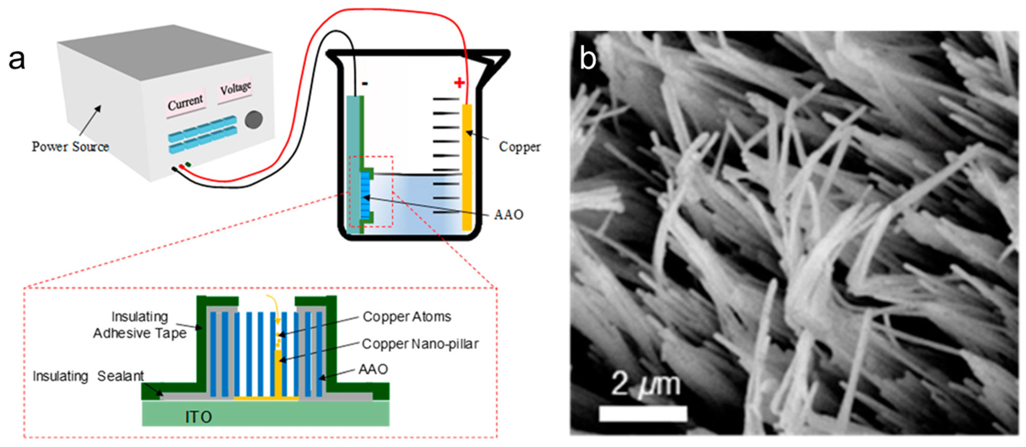
Template-assisted synthesis involves growing Cu NWs by depositing copper atoms into nanoscale pores within a template. Commonly used templates include anodic aluminum oxide (AAO) and porous silicon, with AAO being the most widely utilized. Generally, this method involves three essential steps. First, a porous substrate must be prepared. The substrate needs to be coated with a conductive layer or attached to a conductive film to serve as the seed layer for electrodeposition. Next, an electrodeposition process is carried out to grow Cu nanowires (NWs) within the pores of the porous substrate. Finally, the porous substrate must be removed. Hang et al. optimized key electrodeposition parameters, including current density and temperature, enabling the successful fabrication of Cu nanowires (NWs) in anodic aluminum oxide (AAO) (Figure 1) [54]. In 2001, Gao et al. successfully synthesized Cu NWs within AAO nanopores using constant voltage electrodeposition [55]. Cu NWs of uniform diameter can be obtained in this way. The crystal structure could be controlled by adjusting the deposition voltage, enabling the formation of Cu NWs with a single-crystal structure at low voltage. Wojciech et al. reported the fabrication of Cu NWs through a similar electrochemical deposition process. The copper atoms were deposited into anodic aluminum oxide (AAO) templates using a solution of 0.3 M copper sulfate and 0.1 M boric acid at a potential of −0.3 V for 30 min [56]. This process was preceded by an optimized electrochemical barrier layer thinning to enhance conductivity at the pore bottoms, ensuring effective deposition of copper ions. The resulting Cu NWs had an average diameter of approximately 35–40 nm and lengths ranging from 14 to 16 μm, demonstrating improved uniformity and quality. Cu NWs can also be deposited within porous silicon templates. Newsha et al. reported that the copper microwires were successfully grown by electrodeposition, starting from the bottom of the pores in the silicon [57]. The resulting wires had a diameter of approximately 3 µm and a length of about 20 µm. The template-assisted synthesis method is very simple and cheap, not necessitating expensive equipment. However, template-assisted synthesis is not well-suited for large-scale production due to several limitations. First, the size of the nanowires is constrained by the template dimensions, which must be prefabricated, adding complexity and cost. Second, removing the template after nanowire formation can potentially damage the structures. Third, since this method does not involve surfactant coating, the resulting nanowires are prone to agglomeration, further hindering their practical application.
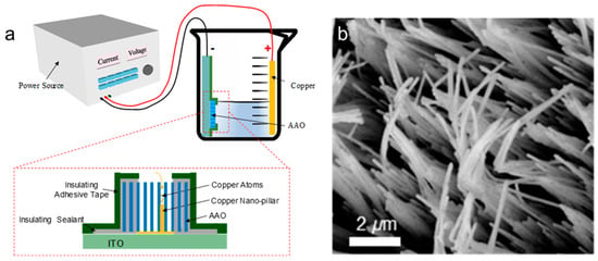
Figure 1.
Synthesis of Cu NWs by template assisted method. (a) Schematic illustration of the template-assisted method; (b) top view of a Cu NW array [54].
2.2. Hydrazine Method
Hydrazine has proven to be an effective reducing agent for the rapid and large-scale synthesis of Cu NWs at low temperatures in air. In 2005, Zeng’s group developed a hydrazine method for synthesizing copper nanowires (Cu NWs) with diameters ranging from 60 to 160 nm, utilizing hydrazine as a reducing agent and ethylenediamine (EDA) as a capping agent at a temperature of 80 °C for one hour [58]. Harsojo et al. investigated the roles of hydrazine (reducing agent) and ethylenediamine (EDA, capping agent) in the wet chemical synthesis of copper nanowires (Cu NWs). Using Cu(NO₃)2·3H2O as a precursor in a highly alkaline solution (15 M NaOH), the authors optimized the reaction by varying hydrazine (0.15–0.75 mL) and EDA (0.5–1.5 mL) volumes at 60 °C. Key findings reveal that EDA guides nanowire growth by chelating Cu2+ ions, while hydrazine controls the reduction kinetics (Figure 2) [59]. The optimal ratio (0.15 mL hydrazine + 1.5 mL EDA) yields Cu NWs with a high aspect ratio (~120 ± 30). The reaction took place in an alkaline environment facilitated by the addition of sodium hydroxide, leading to the formation of metallic copper as outlined in the following reaction:
2Cu2+ + N2H4 + 4OH−→2Cu + N2 + 4H2O
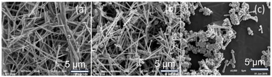
Figure 2.
Synthesis of Cu NWs through the hydrazine method. The morphologies of Cu NWs synthesized with different hydrazine volumes: (a) 0.15 mL; (b) 0.25 mL; (c) 0.35 mL [59].
In 2010, Wiley’s group scaled up this reaction by a factor of 200. Upon completion, the solution underwent a color change from blue to reddish-brown, indicating the synthesis of Cu NWs [49]. Yan et al. described another straightforward approach to grow Cu NWs on glass substrates, where CuCl2·2H2O provided copper ions, and polyvinylpyrrolidone (PVP) served as a capping agent to control the growth direction of the seed crystals. In this method, hydrazine reduced Cu2+ to metallic copper, with the precursor solution flowing through a continuous flow reactor that housed the growth substrate [60]. The researchers concluded that EDA selectively bound to the side facets of the crystals, directing the anisotropic growth of the Cu NWs, with copper atoms depositing at the ends to elongate the structures. This synthesis method demonstrates significant advantages in terms of simplicity, rapid processing time, and cost-effectiveness, making it highly suitable for large-scale production. However, the utilization of hydrazine as a reducing agent presents notable toxicity concerns. Consequently, there is a pressing need to develop more environmentally benign alternatives to maintain the method’s practical advantages while addressing its environmental limitations.
2.3. Hydrothermal Method
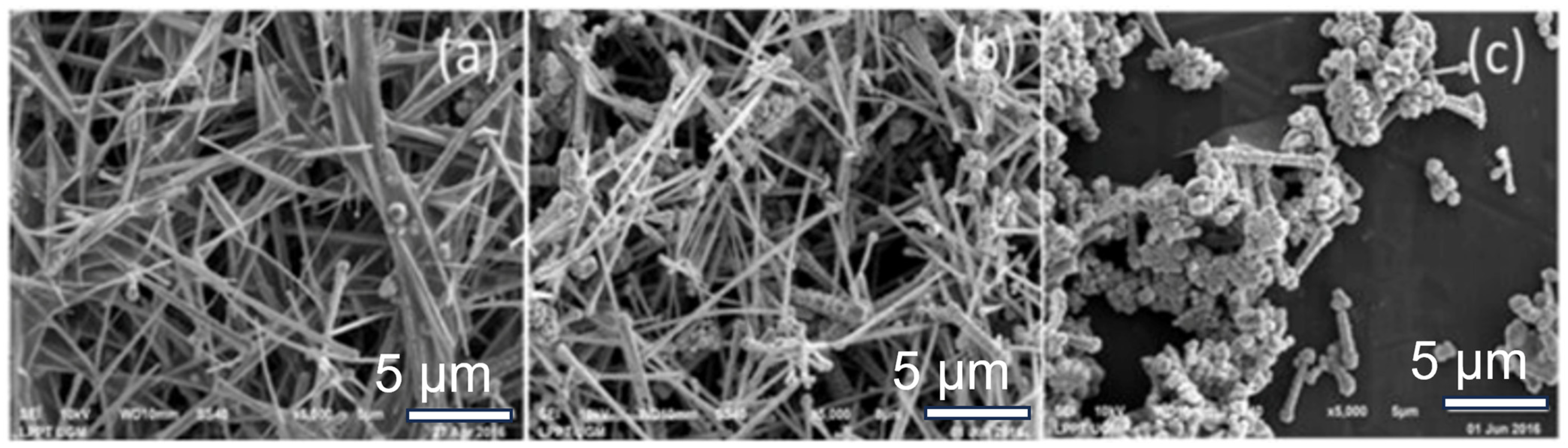
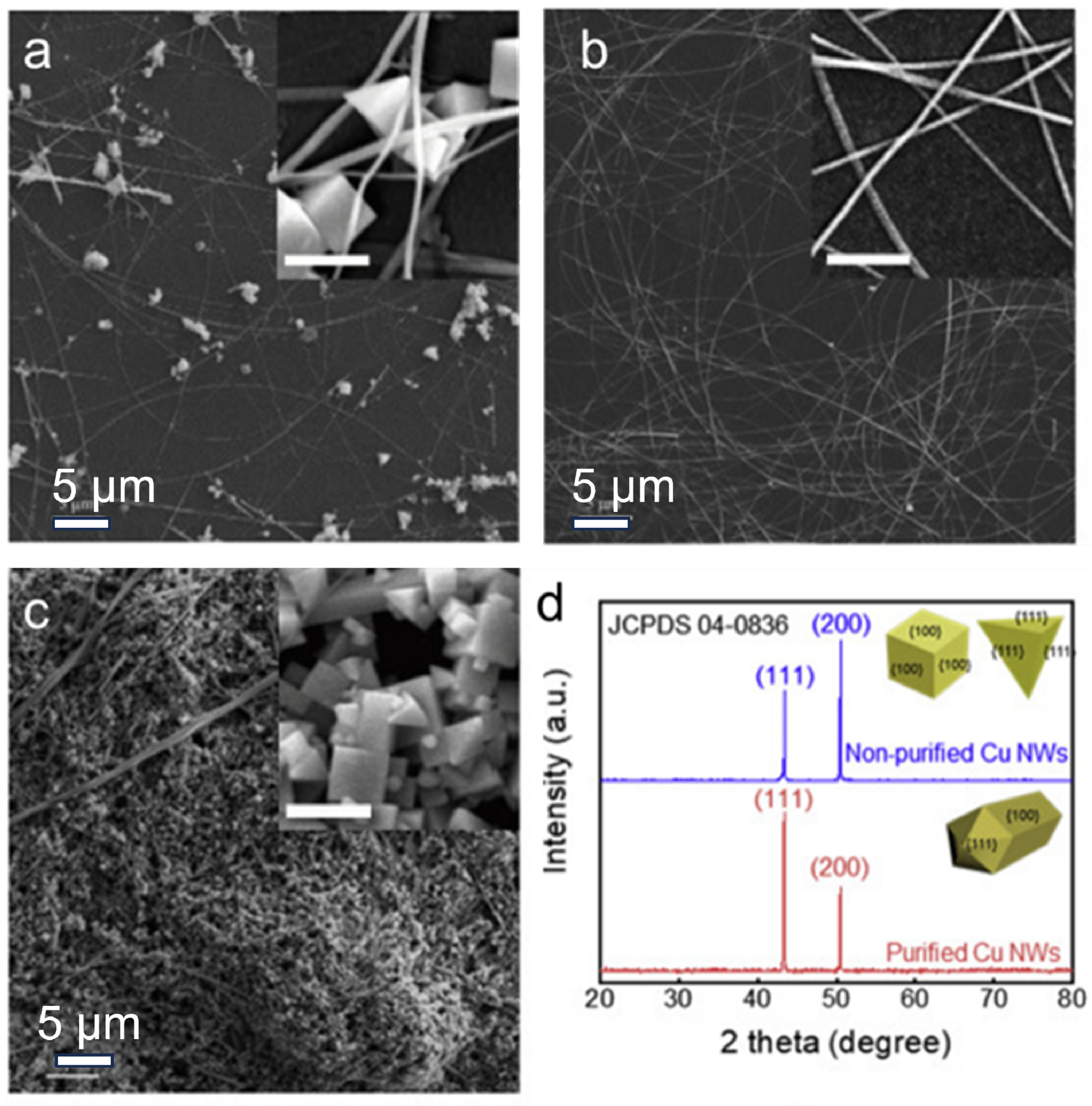
The hydrothermal method is a widely adopted approach for synthesizing nanomaterials, utilizing an aqueous solution as the reaction environment. Xia’s team developed a straightforward hydrothermal synthesis technique to produce Cu NWs with an average diameter of 24 nm [61]. In this process, hexadecylamine (HDA) acted as a selective capping agent, demonstrating strong affinity for the (100) crystal facets of Cu. Initially, Cu2+ ions formed a complex with HDA under vigorous stirring at room temperature, followed by reduction to Cu0 through glucose. Several studies have also investigated low-carbon-chain amines for similar applications. In 2014, Yang et al. reported the synthesis of five-fold twinned Cu NWs via a self-seeded growth mechanism, employing oleylamine (OLA) as a capping agent [62]. Their findings indicated that OLA preferentially binds to the (100) facets of Cu crystals, influencing their growth. Subsequently, Shi et al. fabricated Cu NWs with an exceptionally high aspect ratio (>105) using octadecylamine as both a surfactant and a reducing agent, although this approach required an elevated reaction temperature of 160 °C [63]. Jiang et al. successfully synthesized ultra-long, pencil-like Cu NWs with a uniform diameter of 45 nm via a hydrothermal process [64]. To enhance the purity of Cu NWs, Zhang et al. introduced a straightforward purification technique, effectively separating nanowires from nanoparticles through liquid–liquid extraction using water and n-hexane [65]. High-purity Cu NWs can be obtained in this way, as shown in Figure 3. In this synthesis, CuCl2 serves as the copper precursor, while glucose functions as the reducing agent and HDA controls the directional growth of copper atoms. The reaction proceeds for 24 h at 120 °C under hydrothermal conditions. This green and facile approach enables efficient large-scale production of Cu NWs. The obtained high-aspect-ratio nanowires facilitate fabrication of FTCs with low Cu NW loading, demonstrating significant potential for applications in display technologies, photovoltaic devices, and smart window systems.
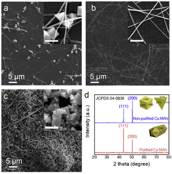
Figure 3.
Synthesis of Cu NWs through the hydrothermal method. (a) As-prepared Cu NWs; (b) Cu NWs after purification; (c) filtrate; (d) XRD of purified and non-purified Cu NWs [65].
3. Methods for Enhancing the Conductivity of Cu Nanowire Networks
Remarkable conductivity is a key criterion for evaluating FTCs. In metal-based NW FTCs, resistance primarily originates from two factors: the intrinsic resistance of the NWs and the contact resistance between stacked NWs. Despite their nanoscale dimensions, metal NWs inherently exhibit excellent electrical conductivity. As a result, the overall electrical performance is largely governed by contact resistance, making tight connections between stacked NWs essential for expanding the conductive pathways. In this section, we review methods for enhancing their electrical performance.
3.1. Heating Method for Cu Nanowire Joining
The heating method is a highly versatile approach for improving the performance of nanowire junctions and is also the most commonly used approach for this purpose. It is applicable to various types of metal nanowires. When materials reach the nanoscale, their melting points significantly decrease with reduced particle size. As a result, nanomaterials can be interconnected at temperatures far below their bulk melting points. For instance, copper nanowires (Cu NWs) can be effectively joined at 200 °C or even lower temperatures, leading to enhanced electrical conductivity. In 2013, Peng et al. applied thermal sintering treatment to Cu NW electrodes at 150 °C and 200 °C, significantly enhancing electrode conductive performance (Figure 4a,b) [66]. At a transmittance of 93%, the sheet resistance was reduced to just 51 Ohm/sq. During the heating process, the organic coating on the surface of the metal nanowires decomposes, and the overlapping regions of the nanowires undergo fusion, increasing the contact area between them. This results in stronger junctions, reduced contact resistance, and improved optoelectronic performance of FTCs. The advantages of the heating method primarily lie in its simplicity, convenience, and cost-effectiveness. However, in the thermal sintering process of Cu NWs, a protective gas atmosphere is required to prevent oxidation and reduce any copper oxides formed during heating. Additionally, heating the entire substrate can cause thermal damage if the temperature is too high. For example, PET, one of the most commonly used substrates, begins to deform and degrade at temperatures exceeding 150 °C. Furthermore, nanowires exhibit Rayleigh instability, making them susceptible to structural damage at elevated temperatures. When the temperature is sufficiently high, nanowires may break down and transform into discontinuous nanoparticles.
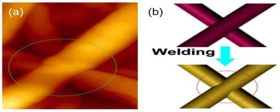
Figure 4.
Joining of Cu NWs through the heating method. (a) Atomic force microscope (AFM) images of welded, stacked Cu NWs; (b) schematic illustration of the joining process between Cu NWs resulting from the heating method [66].
3.2. Laser Sintering for Cu Nanowire Bonding
The laser sintering method utilizes laser energy to achieve sintering at nanowire junctions. Due to the surface plasmon resonance effect, the overlapping regions of nanowires rapidly melt and fuse, significantly enhancing the conductivity of FTCs. Laser joining is an advanced, non-contact bonding technique that utilizes a focused laser beam to generate localized heat at the interface of materials, enabling precise and efficient connection. Compared to traditional bonding methods such as adhesive bonding or thermal compression, laser joining offers several advantages, including high spatial resolution, minimal thermal damage to surrounding areas, rapid processing speed, and compatibility with automation. This technique is particularly suitable for joining nanomaterials—such as nanoparticles and nanowires. Moreover, the localized heating nature of laser joining reduces the risk of thermal degradation, making it a promising method for integrating temperature-sensitive substrates. In 2012, Lee et al. employed laser sintering to weld ultralong silver nanowires, achieving a sheet resistance of just 9 Ohm/sq at a transmittance of 89% [67]. Similarly, in 2014, Han et al. used laser irradiation to sinter Cu NW networks, resulting in a strong bonding between adjacent NWs and a substantial conductive performance improvement [68]. Tran et al. introduced a novel method for fabricating high-quality copper nanowire (Cu NW) transparent conductive electrodes (TCEs) using pulsed laser irradiation. This technique utilizes laser-induced plasmonic heating to weld nanowire junctions (Figure 5), followed by a rapid acetic acid treatment to remove residuals, effectively addressing issues such as high sheet resistance and the presence of residual film-forming agents (from polyvinyl alcohol-based inks). The optimized process achieves low sheet resistance (34–199 Ω/sq) and high transmittance (81.2%–87.3%) within just 15 min, outperforming conventional oven heating methods. The resulting electrodes were successfully applied to touch sensors, demonstrating strong potential for industrial applications in flexible electronics and touchscreens [69]. Since lasers have a single wavelength, they deliver highly concentrated energy and enable rapid heating, minimizing damage to the substrate. However, laser sintering must be performed point by point due to its limited irradiation area, leading to low processing efficiency.
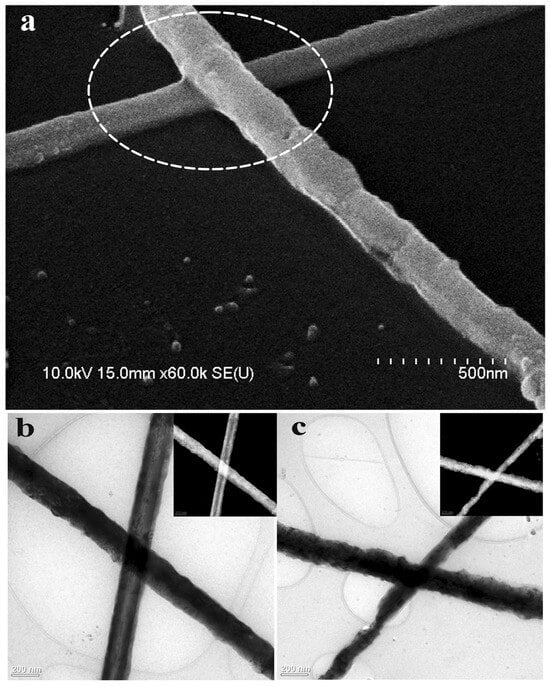
Figure 5.
Joining of Cu NWs by laser. (a) SEM images of joints between Cu NWs by laser; TEM images of Cu NW junction before (b) and after (c) laser joining [69].
3.3. Acid Treatment for Surface Cleaning and Conductivity Improvement
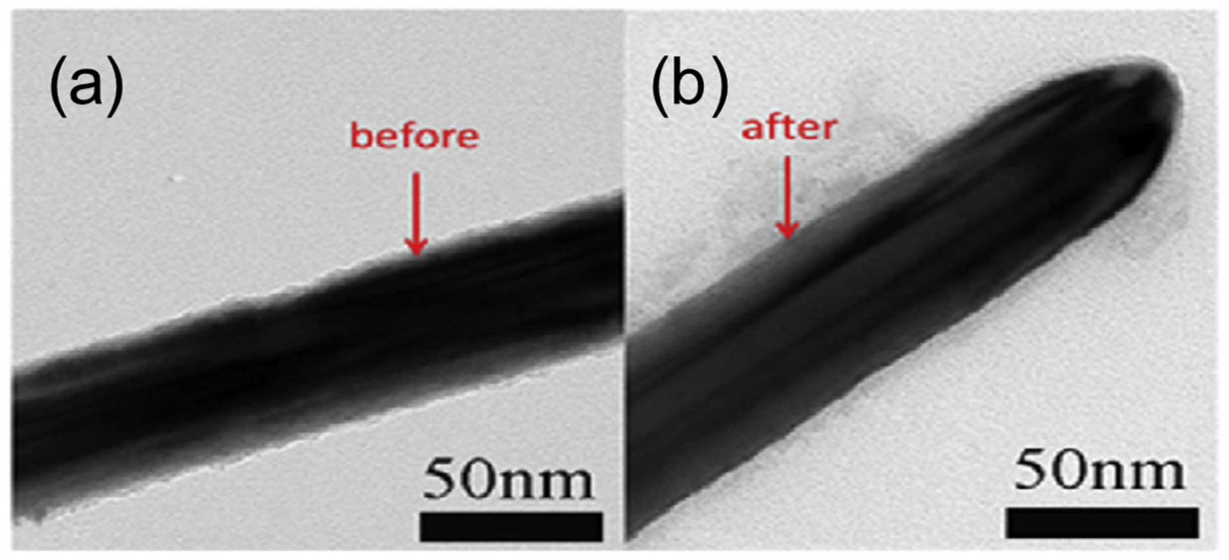
Acid treatment is an effective method for improving the performance of Cu NWs. It removes surface oxides and residual organic compounds, thereby enhancing the electrical conductivity of Cu NW networks. Common acids such as acetic acid or hydrochloric acid are used to selectively etch oxidation layers without damaging the nanowire structure. This simple, low-cost process is crucial for maintaining long-term stability and achieving high-performance transparent conductive electrodes in flexible electronics and optoelectronic devices. In 2014, Mayousse et al. treated Cu NW-based FTCs with acetic acid, achieving a sheet resistance of just 9 Ohm/sq at a transmittance of 88%, a value comparable to the performance of some silver nanowire electrodes [70]. In 2016, Wang et al. soaked Cu NW FTCs in acetic acid for 30 s, improving their electrical performance from being initially non-conductive to a sheet resistance of 185 Ohm/sq [71]. Additionally, since acid treatment thins the nanowires (Figure 6), it also slightly enhances transmittance. However, acid treatment can easily damage Cu NWs and lead to severe secondary oxidation. Therefore, it is typically used in combination with protective coatings to mitigate these effects.

Figure 6.
TEM images (a) before and (b) after acid treatment [71].
3.4. Photonic Sintering for Efficient Nanowire Welding
The photonic sintering method utilizes full-spectrum light irradiation to form strong junctions between nanowires. Photonic sintering is an efficient technique for nanoscale interconnection. By exposing nanostructures to light sources, localized plasmonic effects at the junctions of nanowires induce surface melting or fusion, enabling effective bonding without damaging the surrounding substrate. This approach allows for rapid welding of nanomaterials, significantly enhancing the electrical conductivity of the network while maintaining structural integrity. Compared to conventional thermal annealing, photonic sintering offers several advantages, including reduced processing time, lower thermal budget, and compatibility with heat-sensitive or flexible substrates. It holds great potential for large-scale fabrication of high-performance transparent conductors, flexible electronics, and wearable devices. This process can be conducted at room temperature with high efficiency. Photonic sintering takes advantage of the plasmonic effect in noble metal nanowires. The high-energy ultraviolet (UV) component of the spectrum removes organic residues and oxide layers from the nanowire surface, while the infrared (IR) component provides thermal energy to melt and fuse the overlapping regions, establishing strong connections. In 2016, Ding et al. successfully fabricated high-performance Cu NW FTCs using photonic sintering [72]. The Cu NWs are effectively connected due to the localized plasmonic exciton effect, as shown in Figure 7. At a transmittance of 85%, the sheet resistance was reduced to just 34.1 Ohm/sq. Since photonic sintering operates at room temperature and under ambient conditions, it is a simple, feasible, and effective sintering method. Ding et al. successfully fabricated high-conductivity FTC on the surface of thermally sensitive substrates by using the photopolymerization sintering method. This indicates that this method can effectively connect copper nanowires without damaging the substrate (Figure 7) [73]. This method enables rapid localized heating at nanowire junctions through photothermal effects, achieving efficient welding under ambient conditions. The resulting flexible transparent conductor exhibits a sheet resistance of 128 Ohm/sq and a transmittance exceeding 95% at 560 nm on PET substrates. The WFL technique offers high processing efficiency, substrate compatibility, and scalability, making it a promising approach for fabricating flexible optoelectronic devices.
Figure 7.
Joining of Cu NWs by photonic sintering [73].
In short, interconnecting the copper nanowires can effectively reduce contact resistance and improve conductivity. The summary of the sheet resistance and light transmittance of the transparent electrodes obtained by various processing methods is shown in Table 1.

Table 1.
Summary of sheet resistance and transmittance of Cu NW FTCs after treatment with different methods.
4. Improve Antioxidant Properties
In addition to the aforementioned improvements in joint properties to enhance the conductivity of FTCs, incorporating a protective layer to improve antioxidant properties is also crucial. Copper, being highly susceptible to oxidation even under atmospheric conditions, is particularly vulnerable at the nanoscale. The formation of an oxidized layer hinders electron transmission, resulting in a rapid decline in the electrical conductivity of FTCs. To address this issue, researchers have explored various solutions.
4.1. Noble Metal Core–Shell Protective Layer
The noble metal core–shell protective layer involves forming a chemically stable, oxidation-resistant metal coating around Cu NWs. Among the most commonly used materials for this purpose are silver and gold shell layers. Generally, core–shell nanowires can be prepared using two methods: galvanic replacement reactions and electroplating.
4.1.1. Galvanic Replacement Reactions
The preparation of FTCs using galvanic replacement reactions typically requires first the synthesis of core–shell structured nanowires, followed by the preparation of electrodes. In 2019, Zhang et al. fabricated a Cu@Ag NW network with a core–shell structure by mixing Cu NWs with an Ag-amine complex, followed by high-energy pulsed light treatment to induce alloying between Cu and Ag (Figure 8) [74]. The resulting nanowire FTCs retained stable conductivity for 500 h under conditions of 85 °C and 85% relative humidity. Koga et al. fabricated Cu@Ag NW transparent electrodes using a vacuum filtration and transfer method on polymer-coated glass substrates [75]. To enhance adhesion, the nanowires were pressed onto the substrate using capillary immersion force, which improved contact between the NWs and the polymer surface. The resulting flexible transparent electrodes exhibited excellent performance, with a transmittance of 89.4% and a sheet resistance of 61.3 Ohm/sq. Additionally, the Cu@Ag NW films demonstrated high durability, retaining stable conductivity even under spin-coating conditions. Their oxidation resistance was enhanced by the Ag shell, ensuring long-term stability. Chu et al. developed ultra-stable Cu@Ag core–shell nanowires (NWs) via galvanic replacement to enhance thermal stability and conductivity for wearable electronics. The Ag coating prevented oxidation, enabling the production of durable transparent heaters and strain sensors with high sensitivity [76]. The NWs also exhibited robust antibacterial properties, making them promising for flexible and healthcare applications. In 2017, Yang Peidong’s group developed FTCs using one-dimensional nanowires with a copper–gold core–shell structure. Even after 1000 bending cycles, the FTCs exhibited minimal changes in sheet resistance, with only a slight increase [77].
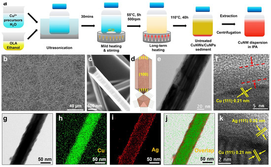
Figure 8.
Fabrication of Cu@Ag core–shell NWs. (a) Schematic illustration of the synthesis of Cu NWs; (b,c) SEM images of Cu NWs; (d) schematic illustration of Cu NWs; (e) TEM and (f) HR-TEM of a Cu NW; (g) SEM image of a Cu@Ag NW and corresponding elemental distribution of (h) Cu, (i) Ag, and (j) both; (k) HR-TEM of a Cu@Ag NW [76].
4.1.2. Electroplating
Since the Cu NW network has some initial electrical conductivity, protective materials can be introduced on its surface with the help of electroplating. Unlike the direct introduction of protective materials, this approach also allows for the simultaneous realization of connections between the Cu NWs to improve electrical conductivity. Zhang et al. presented a method for fabricating Cu NWs coated with a nickel (Ni) layer through electrodeposition, resulting in a core–shell structure known as Cu@Ni [6]. The resulting FTCs exhibited significant improvements in performance, including a dramatic decrease in sheet resistance from 513 OHM/sq to 15.8 OHM/sq at a transmittance of 88%, indicating excellent electrical conductivity. The Ni coating enhanced the junctions between Cu NWs, leading to improved mechanical stability, with only a 1.03-fold increase in resistance after 2000 bending cycles. Furthermore, the Cu@Ni FTC retained stable conductivity after 168 h in an atmospheric environment, while uncoated Cu NWs experienced a tenfold increase in resistance. The films also demonstrated remarkable resistance to corrosion, remaining intact after exposure to 15% H2O2 for 450 s, and retained their structure after being heated to 400 °C for 30 min. The metal co-deposition approach also allows for the cladding of an alloy protective layer on the surface of Cu NWs. For example, Zhang et al. deposited a uniform Ag-Au alloy shell on the Cu NWs, significantly enhancing the stability of the FTCs (Figure 9) [78]. The resulting FTCs exhibited a low sheet resistance of 14.2 Ohm/sq at a transmittance of 90.1%. The coated FTCs demonstrated excellent resistance to oxidation and corrosion, remaining stable after prolonged exposure to harsh environments, including atmospheric conditions and corrosive agents like H2O2 and H2SO4. In addition to their improved stability, the Cu NW@alloy FTCs maintained remarkable mechanical flexibility, successfully enduring 2000 bending cycles without significant resistance changes. The authors also fabricated a bifunctional device that combined electrochromic and supercapacitor functionalities using the Cu NW@alloy FTCs, showcasing their potential for applications in flexible electronics.
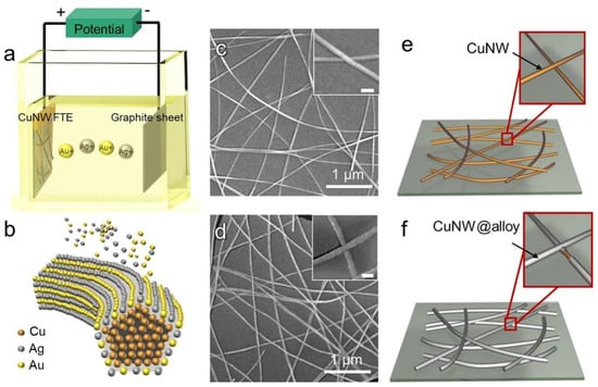
Figure 9.
Electroplating to protect Cu NWs. (a) Schematic illustration of the equipment; (b) schematic illustration of atomic movement during the electroplating process; (c,d) SEM images of the Ag-Au layer (c) before and (d) after electroplating; (e,f) schematic illustrations of the joints between stacked Cu NWs (e) before and (f) after electroplating of the Ag-Au layer [78].
4.2. Poly(3,4-ethylenedioxythiophene):poly(styrenesulfonate)
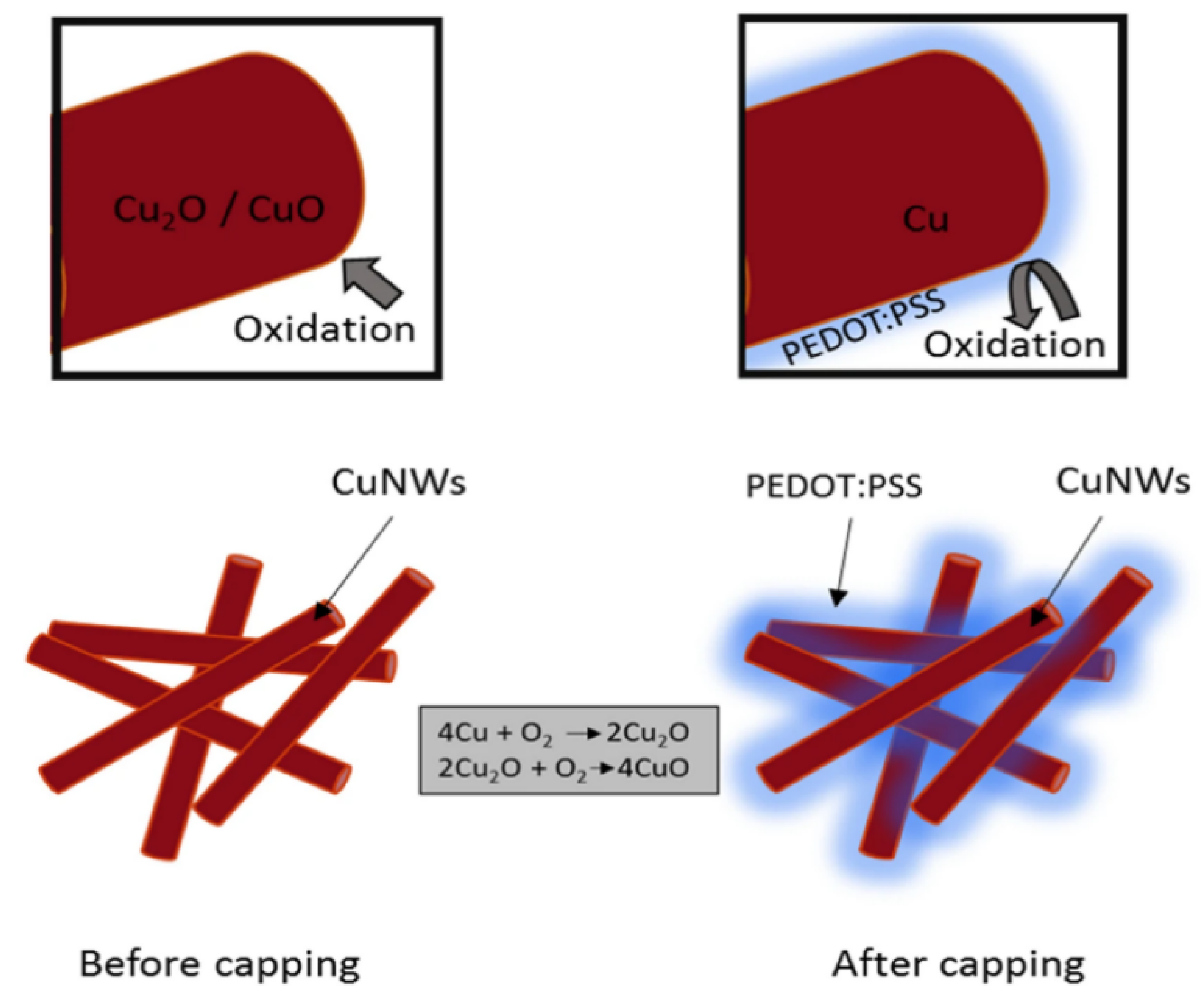
Poly(3,4-ethylenedioxythiophene):poly(styrenesulfonate) (PEDOT:PSS) is a conductive polymer widely used in electronic and optoelectronic applications due to its excellent conductivity, transparency, and flexibility. It consists of positively charged PEDOT chains and negatively charged PSS chains that form stable water-dispersed complexes. PEDOT:PSS is commonly used as transparent electrodes, hole-transporting layers, and antistatic coatings for devices such as organic solar cells, flexible displays, and bioelectronics. Post-treatment with solvents such as DMSO or ethylene glycol can significantly improve its electrical conductivity, making it a versatile material for next-generation electronic applications. The antioxidant properties of PEDOT:PSS allow it to be used as a protective material for Cu NWs. Mayousse et al. reported a highly conductive Cu NW and PEDOT:PSS hybrid electrode with a sheet resistance of 46 Ohm/sq at an optical transmittance of 93% [70]. Similarly, Mardiansyah et al. improved the oxidation resistance of Cu NWs by coating them with a conductive layer of PEDOT:PSS using the Mayer rod method (Figure 10) [79]. This protective layer effectively prevented oxidation while maintaining the excellent conductivity of Cu NWs, overcoming the limitations of previous methods that reduced electrical performance. The resulting transparent FTCs exhibited stable conductivity over an extended period, significantly outperforming uncoated Cu NWs in terms of oxidation resistance.
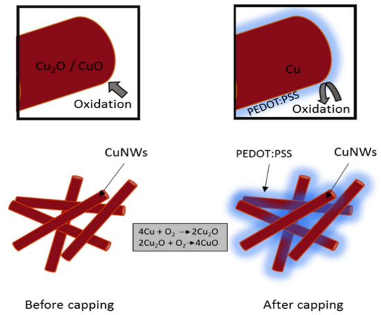
Figure 10.
Preventing copper oxidation with PEDOT:PSS protective layer [79].
4.3. Graphene
Graphene is a two-dimensional material composed of a single layer of carbon atoms arranged in a hexagonal lattice [20]. It exhibits extraordinary electrical, mechanical, and thermal properties, making it one of the most promising materials in nanotechnology. Graphene has exceptional electrical conductivity, high carrier mobility, and excellent mechanical strength while remaining lightweight and flexible. Its transparency and chemical stability also make it suitable for applications in flexible electronics, energy storage, sensors, and biomedical devices. Graphene exhibits exceptional oxidation resistance due to its densely packed hexagonal carbon lattice, which provides an effective barrier against oxygen diffusion. The material’s chemical inertness and impermeability to gases make it highly resistant to oxidative degradation, even at elevated temperatures. Researchers are developing graphene-based composite coatings that leverage these properties for corrosion protection applications [80]. Yumi et al. developed a Cu NW–graphene nanostructure using a low-temperature plasma-enhanced chemical vapor deposition (LT-PECVD) method [81]. The electrodes were fabricated by first synthesizing Cu NWs via a solution-phase reduction method and then coating them with graphene to enhance their stability. The resulting FTCs exhibited excellent electrical and optical properties, with a sheet resistance of 53.8 Ohm/sq and a transmittance of 89.3% at 550 nm. Compared to bare Cu NW FTCs, the Cu NW–graphene FTCs demonstrated remarkable oxidation resistance, with only a 9% increase in sheet resistance after 30 days under an air atmosphere, while uncoated Cu NWs experienced an 1800-fold increase within 2 days. The Cu NW–graphene FTCs were successfully used in bulk heterojunction polymer solar cells, showing improved power conversion efficiency due to their enhanced stability and conductivity. Zhao et al. prepared the Cu NW–reduced-graphene (rGO) hybrid films through a direct mixing method, where aqueous dispersions of Cu NWs and rGO were combined, followed by membrane filtration to form uniform thin films on PET substrates [82]. The resulting FTCs exhibited excellent electrical and optical properties, achieving a sheet resistance as low as 50 Ohm/sq and a transmittance greater than 80% at 550 nm. Additionally, the hybrid films demonstrated significantly improved oxidation resistance and mechanical flexibility compared to pure Cu NW films. The incorporation of rGO not only enhanced the conductivity and transparency of the films but also reduced the fluctuations in sheet resistance, making them more stable under varying conditions. Lin et al. presented a simple approach for fabricating highly stable FTCs using hydrogen-annealing–reduced-graphene-oxide (h-rGO) and copper nanowires (Cu NWs) (Figure 11). The resulting h-rGO/Cu NW films exhibited excellent oxidation resistance, flexibility, and stable electrical properties, making them promising for future optoelectronic applications [83].
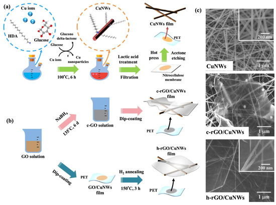
Figure 11.
Fabrication of Cu NW–graphene FTCs. (a) Fabrication process of Cu NWs; (b) fabrication process of h-rGO/Cu NW films; (c) SEM images of Cu NWs, c-rGO/Cu NWs, and h-rGO/Cu NWs [83].
5. Conclusions
In conclusion, Cu NWs represent a promising alternative to traditional transparent conductors due to their favorable electrical properties and cost advantages. While challenges remain, particularly regarding oxidation and conductivity, ongoing research into synthesis techniques and protective coatings shows significant potential for overcoming these issues. The combination of Cu NWs with advanced materials like noble metals and conductive polymers enhances their stability and performance, making them suitable for various flexible electronic applications. As the demand for sustainable and efficient materials continues to grow, Cu NWs are poised to play a vital role in the development of next-generation flexible transparent devices. Currently, to advance the practical applications of Cu NW-based FTCs, researchers are focusing on developing stable, large-scale copper nanowire synthesis methods compatible with advanced technologies like printed electronics and roll-to-roll processing, aiming to create highly conductive and oxidation-resistant electrode materials. Future development priorities include eco-friendly synthesis techniques, as well as mild interconnection and anti-oxidation approaches that align with mass production processes. Integration with functional materials (e.g., perovskites, 2D materials, hydrogels) will enable flexible multifunctional electronic devices. The key challenge lies in balancing cost, durability, and performance to overcome the competition from indium-free alternatives and achieve commercial viability.
Funding
This work was financially supported by the Social Welfare and Basic Research Project of Zhong Shan (No200827093620848).
Institutional Review Board Statement
Not applicable.
Informed Consent Statement
Not applicable.
Data Availability Statement
Data sharing is not applicable. No new data were created or analyzed in this study.
Conflicts of Interest
The authors declare no competing interests.
References
- Nair, N.M.; Khanra, I.; Ray, D.; Swaminathan, P. Silver Nanowire-Based Printable Electrothermochromic Ink for Flexible Touch-Display Applications. ACS Appl. Mater. Interfaces 2021, 13, 34550–34560. [Google Scholar] [CrossRef] [PubMed]
- Li, H.; Geng, W.; Zheng, Z.; Haruna, S.A.; Chen, Q. Flexible SERS sensor using AuNTs-assembled PDMS film coupled chemometric algorithms for rapid detection of chloramphenicol in food. Food Chem. 2023, 418, 135998. [Google Scholar] [CrossRef]
- Ding, S.; Chen, J.; Li, K.; Zhang, H. Fabrication strategies for metallic nanowire flexible transparent electrodes with high uniformity. J. Mater. Chem. A 2024, 12, 18815–18831. [Google Scholar] [CrossRef]
- Wang, P.; Jian, M.; Wu, M.; Zhang, C.; Zhou, C.; Ling, X.; Zhang, J.; Yang, L. Highly sandwich-structured silver nanowire hybrid transparent conductive films for flexible transparent heater applications. Compos. Part A Appl. Sci. Manuf. 2022, 159, 106998. [Google Scholar] [CrossRef]
- Zhang, H.; Zhu, X.; Tai, Y.; Zhou, J.; Li, H.; Li, Z.; Wang, R.; Zhang, J.; Zhang, Y.; Ge, W.; et al. Recent advances in nanofiber-based flexible transparent electrodes. Int. J. Extrem. Manuf. 2023, 5, 032005. [Google Scholar] [CrossRef]
- Zhang, H.; Wang, S.; Tian, Y.; Liu, Y.; Wen, J.; Huang, Y.; Hang, C.; Zheng, Z.; Wang, C. Electrodeposition fabrication of Cu@Ni core shell nanowire network for highly stable transparent conductive films. Chem. Eng. J. 2020, 390, 124495. [Google Scholar] [CrossRef]
- Papanastasiou, D.T.; Schultheiss, A.; Muñoz-Rojas, D.; Celle, C.; Carella, A.; Simonato, J.P.; Bellet, D. Transparent heaters: A review. Adv. Funct. Mater. 2020, 30, 1910225. [Google Scholar] [CrossRef]
- Zhou, Q.; Chen, J.; Zhou, X.; Liu, X.; Lu, X.; Wei, R.; Liu, Y.; Zhang, Z.; Xiong, Z.; Xiong, S.; et al. Relieving strain on silver nanowires embedded in polyimide films for efficient flexible organic photovoltaic modules. J. Mater. Chem. A 2025, 13, 3720–3726. [Google Scholar] [CrossRef]
- Yang, S.; Cao, Y.-J.; Han, K.; Guo, J.-T.; Zheng, P.-L.; Wang, L.-Y.; Cheng, T.; Zhang, Y.-Z.; Lai, W.-Y. Stretchable transparent electrodes based on metal grid hybrids for skin-like multimodal sensing and flexible touch panel. Nano Energy 2025, 139, 110942. [Google Scholar] [CrossRef]
- Salam, A.A.; Ebrahim, S.; Soliman, M.; Shokry, A. Preparation of silver nanowires with controlled parameters for conductive transparent electrodes. Sci. Rep. 2024, 14, 20986. [Google Scholar] [CrossRef]
- Zhang, H.; Tian, Y.; Wang, S.; Feng, J.; Hang, C.; Wang, C.; Ma, J.; Hu, X.; Zheng, Z.; Dong, H. Robust Cu-Au alloy nanowires flexible transparent electrode for asymmetric electrochromic energy storage device. Chem. Eng. J. 2021, 426, 131438. [Google Scholar] [CrossRef]
- Zhang, H.; Tian, Y. Single-atom modification strategy for highly stable electrochromism. Matter 2023, 6, 2591–2594. [Google Scholar] [CrossRef]
- Zhang, H.; Sun, F.; Cao, G.; Zhou, D.; Zhang, G.; Feng, J.; Wang, S.; Su, F.; Tian, Y.; Liu, Y.J.; et al. Bifunctional flexible electrochromic energy storage devices based on silver nanowire flexible transparent electrodes. Int. J. Extrem. Manuf. 2023, 5, 015503. [Google Scholar] [CrossRef]
- Araujo, J.J.; Brozek, C.K.; Liu, H.; Merkulova, A.; Li, X.; Gamelin, D.R. Tunable band-edge potentials and charge storage in colloidal tin-doped indium oxide (ITO) nanocrystals. ACS Nano 2021, 15, 14116–14124. [Google Scholar] [CrossRef] [PubMed]
- Judic, M.; Lonjon, A.; Dantras, E.; Lacabanne, C. Mechano-Electrically Durability of Flexible Transparent Conductive Electrodes from Silver Nanowires/Polymer Nanocomposites. J. Appl. Polym. Sci. 2025, e56883. [Google Scholar] [CrossRef]
- Yang, H.; Bi, Y.; Wang, S.; Wang, C.; Wang, H.; Ye, G.; Feng, J. Ag-Grid and Ag-Nanowires Hybrid Transparent Electrodes to Improve Performance of Flexible Organic Light-Emitting Devices. Photonics 2025, 12, 272. [Google Scholar] [CrossRef]
- Zeng, K.; Wei, W.; Jiang, L.; Zhu, F.; Du, D. Use of carbon nanotubes as a solid support to establish quantitative (centrifugation) and qualitative (filtration) immunoassays to detect gentamicin contamination in commercial milk. J. Agric. Food Chem. 2016, 64, 7874–7881. [Google Scholar] [CrossRef]
- Ma, S.; Wang, M.; You, T.; Wang, K. Using magnetic multiwalled carbon nanotubes as modified QuEChERS adsorbent for simultaneous determination of multiple mycotoxins in grains by UPLC-MS/MS. J. Agric. Food Chem. 2019, 67, 8035–8044. [Google Scholar] [CrossRef]
- Zhou, W.; Li, C.; Sun, C.; Yang, X. Simultaneously determination of trace Cd2+ and Pb2+ based on l-cysteine/graphene modified glassy carbon electrode. Food Chem. 2016, 192, 351–357. [Google Scholar] [CrossRef]
- Xu, Y.; Zhang, W.; Shi, J.; Zou, X.; Li, Y.; Elrasheid, T.H.; Huang, X.; Li, Z.; Zhai, X.; Hu, X. Electrodeposition of gold nanoparticles and reduced graphene oxide on an electrode for fast and sensitive determination of methylmercury in fish. Food Chem. 2017, 237, 423–430. [Google Scholar] [CrossRef]
- Liu, Z.; Wang, X.; Ren, X.; Li, W.; Sun, J.; Wang, X.; Huang, Y.; Guo, Y.; Zeng, H. Novel fluorescence immunoassay for the detection of zearalenone using HRP-mediated fluorescence quenching of gold-silver bimetallic nanoclusters. Food Chem. 2021, 355, 129633. [Google Scholar] [CrossRef] [PubMed]
- Sonawane, J.R.; Jundale, R.; Kulkarni, A.A. Continuous flow synthesis of metal nanowires: Protocols, engineering aspects of scale-up and applications. Mater. Horiz. 2025, 12, 364–400. [Google Scholar] [CrossRef] [PubMed]
- Ebbesen, T.W.; Ajayan, P.M. Large-scale synthesis of carbon nanotubes. Nature 1992, 358, 220–222. [Google Scholar] [CrossRef]
- Bin, Z.; Feng, L.; Yan, Y. Biomimetic metalloporphyrin oxidase modified carbon nanotubes for highly sensitive and stable quantification of anti-oxidants tert-butylhydroquinone in plant oil. Food Chem. 2022, 388, 132898. [Google Scholar] [CrossRef]
- Wang, X.; Xu, Y.; Li, Y.; Li, Y.; Li, Z.; Zhang, W.; Zou, X.; Shi, J.; Huang, X.; Liu, C. Rapid detection of cadmium ions in meat by a multi-walled carbon nanotubes enhanced metal-organic framework modified electrochemical sensor. Food Chem. 2021, 357, 129762. [Google Scholar] [CrossRef]
- Zeng, K.; Chen, B.; Li, Y.; Meng, H.; Wu, Q.; Yang, J.; Liang, H. Gold nanoparticle-carbon nanotube nanohybrids with peroxidase-like activity for the highly-sensitive immunoassay of kanamycin in milk. Int. J. Food Sci. Technol. 2022, 57, 6028–6037. [Google Scholar] [CrossRef]
- Wu, Z.; Chen, Z.; Du, X.; Logan, J.M.; Sippel, J.; Nikolou, M.; Kamaras, K.; Reynolds, J.R.; Tanner, D.B.; Hebard, A.F.; et al. Transparent, Conductive Carbon Nanotube Films. Science 2004, 305, 1273–1276. [Google Scholar] [CrossRef]
- Wu, S.; Duan, N.; Qiu, Y.; Li, J.; Wang, Z. Colorimetric aptasensor for the detection of Salmonella enterica serovar typhimurium using ZnFe2O4-reduced graphene oxide nanostructures as an effective peroxidase mimetics. Int. J. Food Microbiol. 2017, 261, 42–48. [Google Scholar] [CrossRef]
- Qin, C.; Guo, W.; Liu, Y.; Liu, Z.; Qiu, J.; Peng, J. A novel electrochemical sensor based on graphene oxide decorated with silver nanoparticles–molecular imprinted polymers for determination of sunset yellow in soft drinks. Food Anal. Methods 2017, 10, 2293–2301. [Google Scholar] [CrossRef]
- Li, Y.; Li, Y.; Zhang, D.; Tan, W.; Shi, J.; Li, Z.; Liu, H.; Yu, Y.; Yang, L.; Wang, X. A fluorescence resonance energy transfer probe based on functionalized graphene oxide and upconversion nanoparticles for sensitive and rapid detection of zearalenone. LWT 2021, 147, 111541. [Google Scholar] [CrossRef]
- Rong, J.; Zhou, Z.; Wang, Y.; Han, J.; Li, C.; Zhang, W.; Ni, L. Immobilization of horseradish peroxidase on multi-armed magnetic graphene oxide composite: Improvement of loading amount and catalytic activity. Food Technol. Biotechnol. 2019, 57, 260–271. [Google Scholar] [CrossRef]
- Chao, Y.; Pang, J.; Bai, Y.; Wu, P.; Luo, J.; He, J.; Jin, Y.; Li, X.; Xiong, J.; Li, H. Graphene-like BN@ SiO2 nanocomposites as efficient sorbents for solid-phase extraction of Rhodamine B and Rhodamine 6G from food samples. Food Chem. 2020, 320, 126666. [Google Scholar] [CrossRef] [PubMed]
- Zhao, Y.; Ma, Y.; Zhou, R.; He, Y.; Wu, Y.; Yi, Y.; Zhu, G. Highly sensitive electrochemical detection of paraoxon ethyl in water and fruit samples based on defect-engineered graphene nanoribbons modified electrode. J. Food Meas. Charact. 2022, 16, 2596–2603. [Google Scholar] [CrossRef]
- Novoselov, K.S.; Geim, A.K.; Morozov, S.V.; Jiang, D.; Zhang, Y.; Dubonos, S.V.; Grigorieva, I.V.; Firsov, A.A. Electric Field Effect in Atomically Thin Carbon Films. Science 2004, 306, 666–669. [Google Scholar] [CrossRef] [PubMed]
- Li, Y.; Luo, S.; Sun, L.; Kong, D.; Sheng, J.; Wang, K.; Dong, C. A green, simple, and rapid detection for amaranth in candy samples based on the fluorescence quenching of nitrogen-doped graphene quantum dots. Food Anal. Methods 2019, 12, 1658–1665. [Google Scholar] [CrossRef]
- Sharma, A.S.; Ali, S.; Sabarinathan, D.; Murugavelu, M.; Li, H.; Chen, Q. Recent progress on graphene quantum dots-based fluorescence sensors for food safety and quality assessment applications. Compr. Rev. Food Sci. Food Saf. 2021, 20, 5765–5801. [Google Scholar] [CrossRef] [PubMed]
- Zhang, W.; Xu, Y.; Zou, X. Rapid determination of cadmium in rice using an all-solid RGO-enhanced light addressable potentiometric sensor. Food Chem. 2018, 261, 1–7. [Google Scholar] [CrossRef]
- Kim, K.S.; Zhao, Y.; Jang, H.; Lee, S.Y.; Kim, J.M.; Kim, K.S.; Ahn, J.-H.; Kim, P.; Choi, J.-Y.; Hong, B.H. Large-scale pattern growth of graphene films for stretchable transparent electrodes. Nature 2009, 457, 706–710. [Google Scholar] [CrossRef]
- Yuan, W.; Zhu, X.; Zhang, J.; Xu, J.; Zhang, Y.; Cai, J.; Peng, N.; Kan, C. High initial conductivity and oxidation resistance of copper nanowire films via depositing oxalic acid. Phys. Chem. Chem. Phys. 2025, 27, 7177–7188. [Google Scholar] [CrossRef]
- Zuo, W.; Ding, S. Combination of electrical and photonic sintering of silver nanowires for flexible transparent electrode with high transmittance. Mater. Lett. 2025, 383, 137991. [Google Scholar] [CrossRef]
- Zhang, H.; Feng, J.; Sun, F.; Zhou, D.; Cao, G.; Wu, Z.; Wang, S.; Su, F.; Tian, Y.; Tian, Y. An electrochemically stable Ag@Au–Co core–shell nanowire network-based transparent conductor for flexible self-powered Zn-based electrochromic smart devices. Mater. Adv. 2023, 4, 995–1004. [Google Scholar] [CrossRef]
- Karagiorgis, X.; Shakthivel, D.; Khandelwal, G.; Ginesi, R.; Skabara, P.J.; Dahiya, R. Highly Conductive PEDOT:PSS: Ag Nanowire-Based Nanofibers for Transparent Flexible Electronics. ACS Appl. Mater. Interfaces 2024, 16, 19551–19562. [Google Scholar] [CrossRef]
- Lee, J.-Y.; Connor, S.T.; Cui, Y.; Peumans, P. Solution-Processed Metal Nanowire Mesh Transparent Electrodes. Nano Lett. 2008, 8, 689–692. [Google Scholar] [CrossRef]
- Ding, Y.; Xiong, S.; Sun, L.; Wang, Y.; Zhou, Y.; Li, Y.; Peng, J.; Fukuda, K.; Someya, T.; Liu, R.; et al. Metal nanowire-based transparent electrode for flexible and stretchable optoelectronic devices. Chem. Soc. Rev. 2024, 53, 7784–7827. [Google Scholar] [CrossRef]
- Križan, A.E.; Bardet, L.; Zimny, K.; Romanus, M.; Berthe, M.; Labrugère-Sarroste, C.; Bellet, D.; Tréguer-Delapierre, M. Oxidation-Resistant Cu-Based Nanowire Transparent Electrodes Activated by an Exothermic Reduction Reaction. ACS Nano 2024, 18, 34902–34911. [Google Scholar] [CrossRef] [PubMed]
- Tang, B.; Liu, H.; Liu, B.; Yang, Y.; Yang, P.; Dong, H.; Zhao, L.; Yu, S. Investigation on preparation and performance of high-reliable ZnO–NiO@Cu NW flexible transparent conductive thin films. J. Mater. Sci. Mater. Electron. 2024, 35, 532. [Google Scholar] [CrossRef]
- Kumar, S.; Seo, Y. Flexible Transparent Conductive Electrodes: Unveiling Growth Mechanisms, Material Dimensions, Fabrication Methods, and Design Strategies. Small Methods 2024, 8, 2300908. [Google Scholar] [CrossRef] [PubMed]
- Mardiansyah, D.; Usna, S.R.A.; Nafisah, S.; Harsojo, H.; Hatika, R.G. Improving the Performance of Transparent Conducting Electrodes Based on Cu Nanowires. Indones. J. Chem. 2024, 24, 7. [Google Scholar] [CrossRef]
- Rathmell, A.R.; Bergin, S.M.; Hua, Y.-L.; Li, Z.-Y.; Wiley, B.J. The Growth Mechanism of Copper Nanowires and Their Properties in Flexible, Transparent Conducting Films. Adv. Mater. 2010, 22, 3558–3563. [Google Scholar] [CrossRef]
- Zhang, H.; Sun, F.; Feng, J.; Ling, H.; Zhou, D.; Cao, G.; Wang, S.; Su, F.; Tian, Y.; Tian, Y. A stable, self-regulating, flexible, ITO-free electrochromic smart window for energy-efficient buildings. Cell Rep. Phys. Sci. 2022, 3, 101193. [Google Scholar] [CrossRef]
- Zhang, H.; Wang, S.; Hang, C.; Tian, Y. Joining of copper nanowires by electrodepositing silver layer for high-performance transparent electrode. Weld. World 2021, 65, 1021–1030. [Google Scholar] [CrossRef]
- Ye, S.; Stewart, I.E.; Chen, Z.; Li, B.; Rathmell, A.R.; Wiley, B.J. How copper nanowires grow and how to control their properties. Acc. Chem. Res. 2016, 49, 442–451. [Google Scholar] [CrossRef] [PubMed]
- Li, W.; Hu, X.; Li, Q.; Shi, Y.; Zhai, X.; Xu, Y.; Li, Z.; Huang, X.; Wang, X.; Shi, J. Copper nanoclusters@ nitrogen-doped carbon quantum dots-based ratiometric fluorescence probe for lead (II) ions detection in porphyra. Food Chem. 2020, 320, 126623. [Google Scholar] [CrossRef] [PubMed]
- Hang, C.; Zhang, H.; Tian, Y.; Wang, C.; Huang, Y.; Zheng, Z.; Wang, C. A Modified Interposer Fabrication Process by Copper Nano-Pillars Filled in Anodic Aluminum Oxide Film for 3D Electronic Package. Appl. Sci. 2018, 8, 2188. [Google Scholar] [CrossRef]
- Tao, G.; Guowen, M.; Yewu, W.; Shuhui, S.; Lide, Z. Electrochemical synthesis of copper nanowires. J. Phys. Condens. Matter 2002, 14, 355. [Google Scholar] [CrossRef]
- Stepniowski, W.J.; Moneta, M.; Karczewski, K.; Michalska-Domanska, M.; Czujko, T.; Mol, J.M.C.; Buijnsters, J.G. Fabrication of copper nanowires via electrodeposition in anodic aluminum oxide templates formed by combined hard anodizing and electrochemical barrier layer thinning. J. Electroanal. Chem. 2018, 809, 59–66. [Google Scholar] [CrossRef]
- Vesali, N.; Erfanifam, S.; Jamilpanah, L.; Hasheminejad, M.; Rahmani, Y.; Mohseni, S.M. Growth behavior of Cu, Ni and Cu/Ni electrodeposited microwires within porous Si. Surf. Coat. Technol. 2019, 364, 16–21. [Google Scholar] [CrossRef]
- Chang, Y.; Lye, M.L.; Zeng, H.C. Large-Scale Synthesis of High-Quality Ultralong Copper Nanowires. Langmuir 2005, 21, 3746–3748. [Google Scholar] [CrossRef]
- Harsojo, H.; Puspita, L.A.; Mardiansyah, D.; Roto, R.; Triyana, K. The Roles of Hydrazine and Ethylenediamine in Wet Synthesis of Cu Nanowire. Indones. J. Chem. 2017, 17, 6. [Google Scholar] [CrossRef]
- Zhao, Y.; Zhang, Y.; Li, Y.; He, Z.; Yan, Z. Rapid and large-scale synthesis of Cu nanowires via a continuous flow solvothermal process and its application in dye-sensitized solar cells (DSSCs). RSC Adv. 2012, 2, 11544. [Google Scholar] [CrossRef]
- Jin, M.; He, G.; Zhang, H.; Zeng, J.; Xie, Z.; Xia, Y. Shape-controlled synthesis of copper nanocrystals in an aqueous solution with glucose as a reducing agent and hexadecylamine as a capping agent. Angew. Chem. Int. Ed. 2011, 50, 10560–10564. [Google Scholar] [CrossRef] [PubMed]
- Yang, H.-J.; He, S.-Y.; Tuan, H.-Y. Self-Seeded Growth of Five-Fold Twinned Copper Nanowires: Mechanistic Study, Characterization, and SERS Applications. Langmuir 2014, 30, 602–610. [Google Scholar] [CrossRef]
- Shi, Y.; Li, H.; Chen, L.; Huang, X. Obtaining ultra-long copper nanowires via a hydrothermal process. Sci. Technol. Adv. Mater. 2005, 6, 761–765. [Google Scholar] [CrossRef]
- Jiang, Z.; Tian, Y.; Ding, S. Synthesis and characterization of ultra-long and pencil-like copper nanowires with a penta-twinned structure by hydrothermal method. Mater. Lett. 2014, 136, 310–313. [Google Scholar] [CrossRef]
- Zhang, H.; Wang, S.; Tian, Y.; Wen, J.; Hang, C.; Zheng, Z.; Huang, Y.; Ding, S.; Wang, C. High-efficiency extraction synthesis for high-purity copper nanowires and their applications in flexible transparent electrodes. Nano Mater. Sci. 2020, 2, 164–171. [Google Scholar] [CrossRef]
- Guo, H.; Lin, N.; Chen, Y.; Wang, Z.; Xie, Q.; Zheng, T.; Gao, N.; Li, S.; Kang, J.; Cai, D.; et al. Copper nanowires as fully transparent conductive electrodes. Sci. Rep. 2013, 3, 2323. [Google Scholar] [CrossRef] [PubMed]
- Lee, J.; Lee, P.; Lee, H.; Lee, D.; Lee, S.S.; Ko, S.H. Very long Ag nanowire synthesis and its application in a highly transparent, conductive and flexible metal electrode touch panel. Nanoscale 2012, 4, 6408–6414. [Google Scholar] [CrossRef]
- Han, S.; Hong, S.; Ham, J.; Yeo, J.; Lee, J.; Kang, B.; Lee, P.; Kwon, J.; Lee, S.S.; Yang, M.Y.; et al. Fast plasmonic laser nanowelding for a Cu-nanowire percolation network for flexible transparent conductors and stretchable electronics. Adv. Mater. 2014, 26, 5808–5814. [Google Scholar] [CrossRef] [PubMed]
- Tran, N.-H.; Duong, T.-H.; Kim, H.-C. A fast fabrication of copper nanowire transparent conductive electrodes by using pulsed laser irradiation. Sci. Rep. 2017, 7, 15093. [Google Scholar] [CrossRef]
- Mayousse, C.; Celle, C.; Carella, A.; Simonato, J.-P. Synthesis and purification of long copper nanowires. Application to high performance flexible transparent electrodes with and without PEDOT:PSS. Nano Res. 2014, 7, 315–324. [Google Scholar] [CrossRef]
- Wang, R.; Ruan, H. Synthesis of copper nanowires and its application to flexible transparent electrode. J. Alloys Compd. 2016, 656, 936–943. [Google Scholar] [CrossRef]
- Ding, S.; Jiu, J.; Gao, Y.; Tian, Y.; Araki, T.; Sugahara, T.; Nagao, S.; Nogi, M.; Koga, H.; Suganuma, K.; et al. One-Step Fabrication of Stretchable Copper Nanowire Conductors by a Fast Photonic Sintering Technique and Its Application in Wearable Devices. ACS Appl. Mater. Interfaces 2016, 8, 6190–6199. [Google Scholar] [CrossRef]
- Ding, S.; Tian, Y.; Jiu, J.; Suganuma, K. Highly conductive and transparent copper nanowire electrodes on surface coated flexible and heat-sensitive substrates. RSC Adv. 2018, 8, 2109–2115. [Google Scholar] [CrossRef]
- Zhang, B.; Li, W.; Nogi, M.; Chen, C.; Yang, Y.; Sugahara, T.; Koga, H.; Suganuma, K. Alloying and Embedding of Cu-Core/Ag-Shell Nanowires for Ultrastable Stretchable and Transparent Electrodes. ACS Appl. Mater. Interfaces 2019, 11, 18540–18547. [Google Scholar] [CrossRef]
- Koga, H.; Yokoyama, S.; Motomiya, K.; Yokoyama, K.; Takahashi, H. Adhesive Cu–Ag core-shell nanowires on polymer-coated glass substrates for fabricating transparent conductive films with durability against spin coating. Colloids Surf. A Physicochem. Eng. Asp. 2023, 660, 130804. [Google Scholar] [CrossRef]
- Kuo, Y.-C.; Fan, J.; Zong, L.; Chen, F.; Feng, Z.; Liu, C.; Wan, T.; Gu, Z.; Hu, L.; Guan, P.; et al. Rational design of robust Cu@Ag core-shell nanowires for wearable electronics applications. Chem. Eng. J. 2024, 496, 154001. [Google Scholar] [CrossRef]
- Niu, Z.; Cui, F.; Yu, Y.; Becknell, N.; Sun, Y.; Khanarian, G.; Kim, D.; Dou, L.; Dehestani, A.; Schierle-Arndt, K.; et al. Ultrathin Epitaxial Cu@Au Core-Shell Nanowires for Stable Transparent Conductors. J. Am. Chem. Soc. 2017, 139, 7348–7354. [Google Scholar] [CrossRef]
- Zhang, H.; Tian, Y.; Wang, S.; Huang, Y.; Wen, J.; Hang, C.; Zheng, Z.; Wang, C. Highly stable flexible transparent electrode via rapid electrodeposition coating of Ag-Au alloy on copper nanowires for bifunctional electrochromic and supercapacitor device. Chem. Eng. J. 2020, 399, 125075. [Google Scholar] [CrossRef]
- Mardiansyah, D.; Badloe, T.; Triyana, K.; Mehmood, M.Q.; Raeis-Hosseini, N.; Lee, Y.; Sabarman, H.; Kim, K.; Rho, J. Effect of temperature on the oxidation of Cu nanowires and development of an easy to produce, oxidation-resistant transparent conducting electrode using a PEDOT:PSS coating. Sci. Rep. 2018, 8, 10639. [Google Scholar] [CrossRef]
- Qiu, Y.; Wang, Z.; Owens, A.C.E.; Kulaots, I.; Chen, Y.; Kane, A.B.; Hurt, R.H. Antioxidant chemistry of graphene-based materials and its role in oxidation protection technology. Nanoscale 2014, 6, 11744–11755. [Google Scholar] [CrossRef]
- Ahn, Y.; Jeong, Y.; Lee, D.; Lee, Y. Copper Nanowire–Graphene Core–Shell Nanostructure for Highly Stable Transparent Conducting Electrodes. ACS Nano 2015, 9, 3125–3133. [Google Scholar] [CrossRef] [PubMed]
- Zhao, F.-G.; Kong, Y.-T.; Xu, Z.-W.; Yao, X.; Zuo, B.; Li, W.-S. High-performance flexible transparent conductive films achieved by cooperation between 1D copper nanowires and 2D graphene materials. J. Mater. Chem. C 2017, 5, 5509–5516. [Google Scholar] [CrossRef]
- Lin, Y.-T.; Huang, D.-W.; Huang, P.-F.; Chang, L.-C.; Lai, Y.-T.; Tai, N.-H. A green approach for high oxidation resistance, flexible transparent conductive films based on reduced graphene oxide and copper nanowires. Nanoscale Res. Lett. 2022, 17, 79. [Google Scholar] [CrossRef] [PubMed]


Disclaimer/Publisher’s Note: The statements, opinions and data contained in all publications are solely those of the individual author(s) and contributor(s) and not of MDPI and/or the editor(s). MDPI and/or the editor(s) disclaim responsibility for any injury to people or property resulting from any ideas, methods, instructions or products referred to in the content. |
© 2025 by the authors. Licensee MDPI, Basel, Switzerland. This article is an open access article distributed under the terms and conditions of the Creative Commons Attribution (CC BY) license (https://creativecommons.org/licenses/by/4.0/).