
Highly Sensitive and Tunable Graphene Metamaterial Perfect Absorber in the Near-Terahertz Band


Abstract
1. Introduction
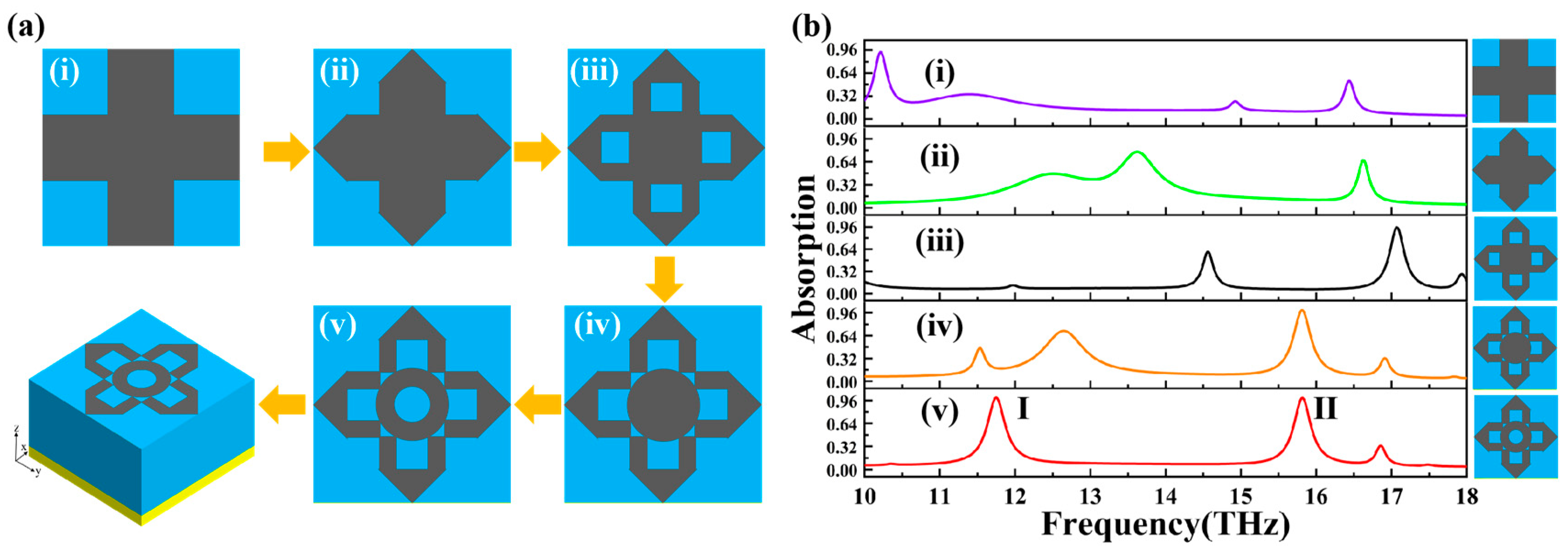
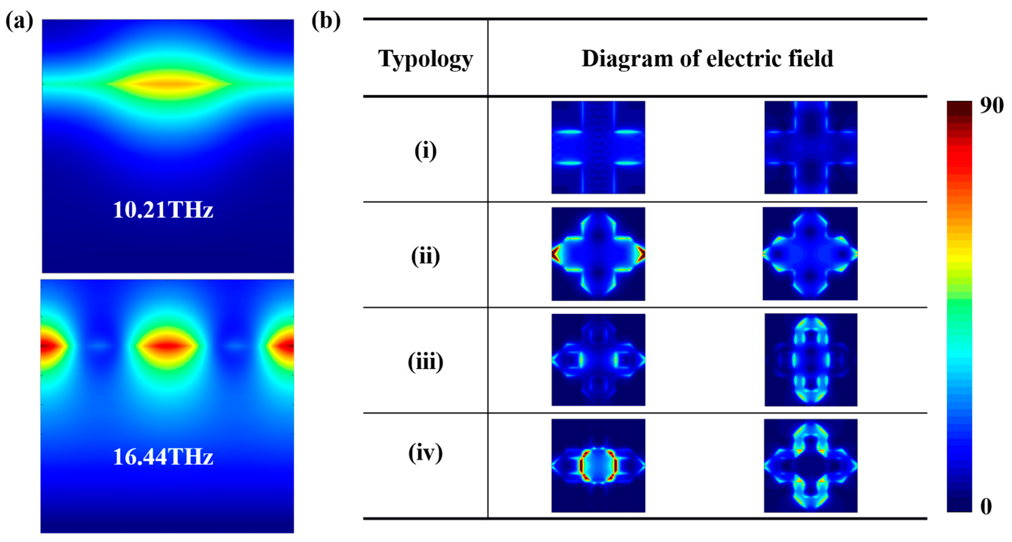
- (i)
- The absorption characteristics of this design are dynamically adjustable. By skillfully adjusting the parameters of the metamaterial, the absorption efficiency of the whole absorber can be effectively affected, which greatly improves the flexibility of the absorber at the design level and the real-time adjustability in actual use.
- (ii)
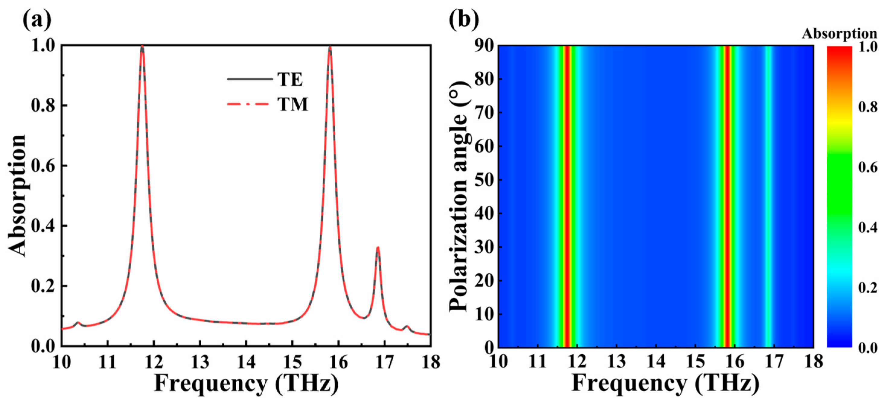
- The absorber is insensitive to the angle of polarization of the incident light (0–90°) and is therefore very practical.
- (iii)
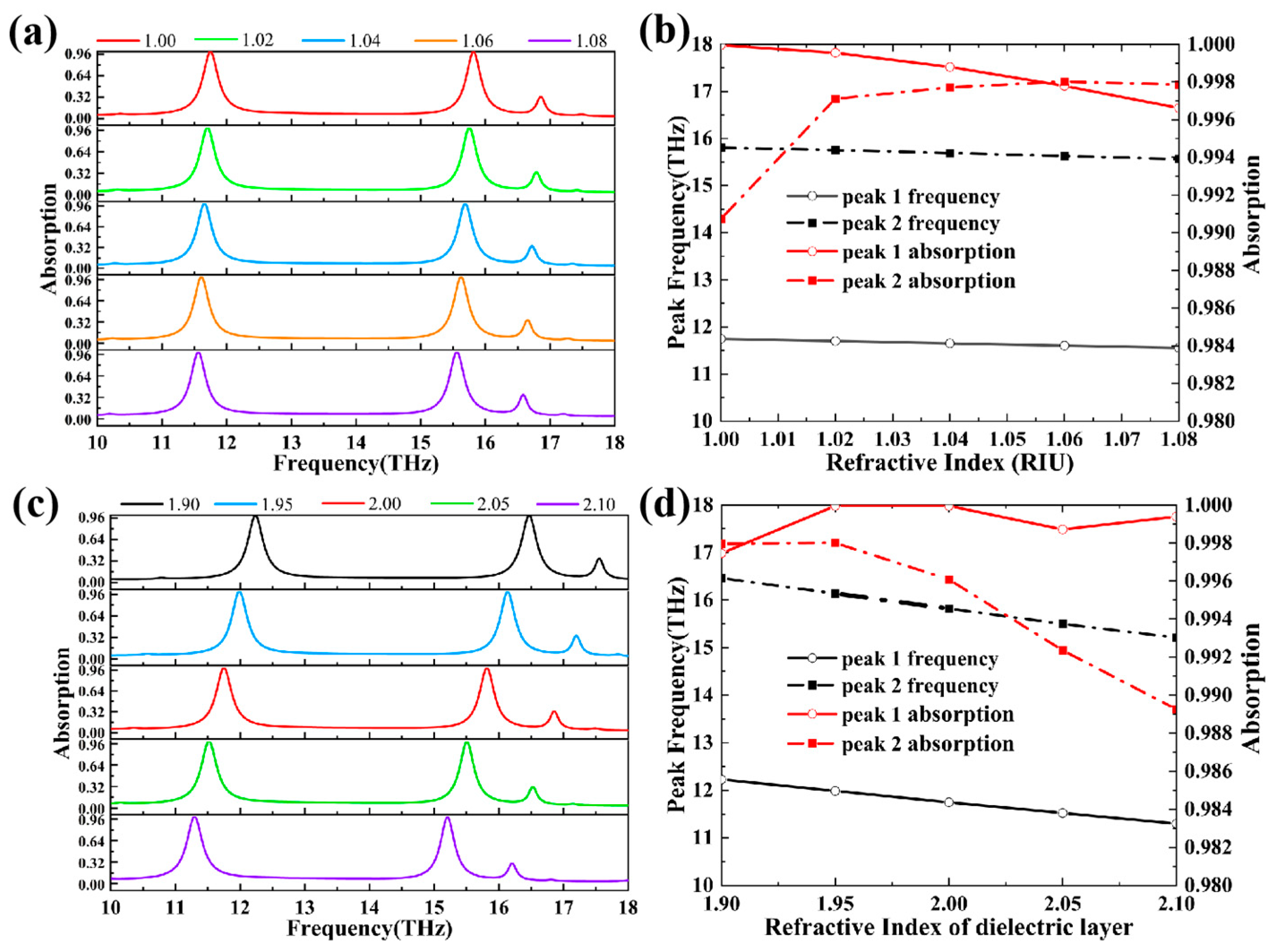
- To comprehensively assess the performance of the design, key parameters such as sensitivity (S), figure of merit (FOM), and quality factor (Q-Factor) are introduced. The design demonstrates exceptional sensing capabilities, supported by its high sensitivity, superior FOM, and high Q-Factor.
- (iv)
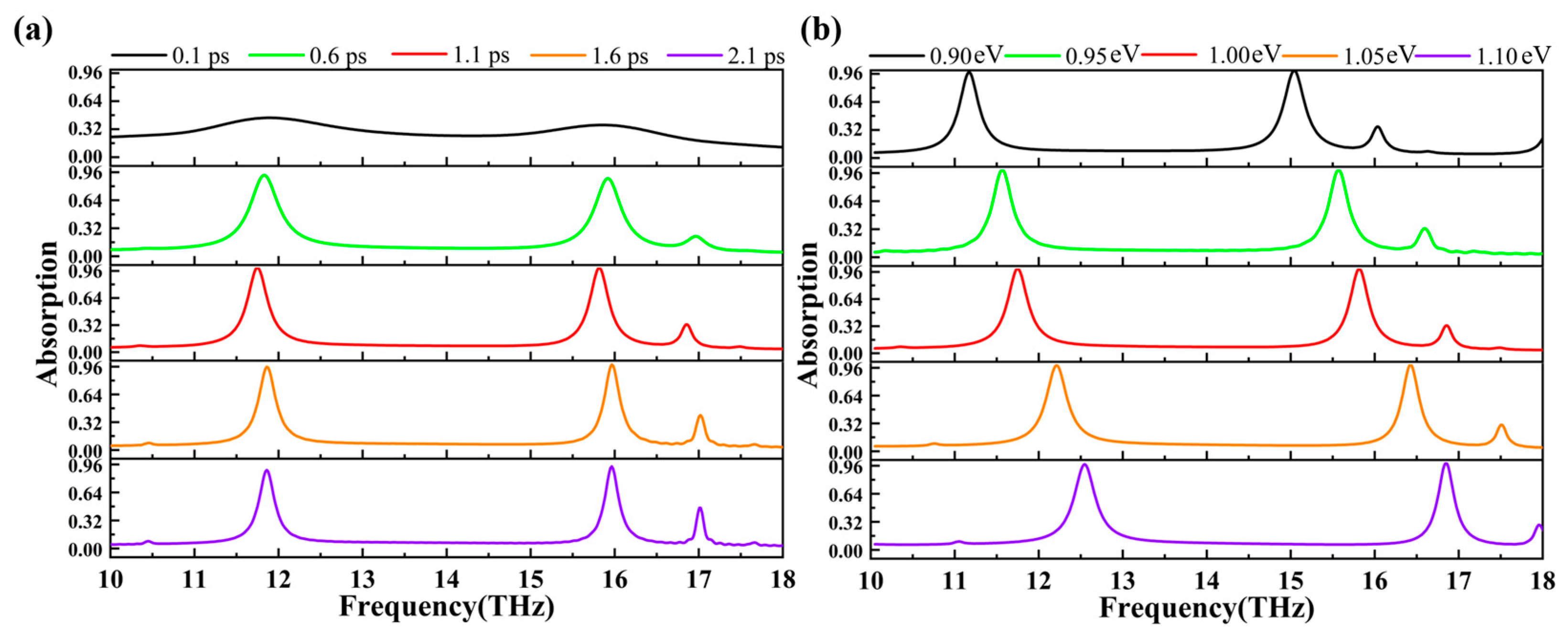
- The design achieves two perfect absorption peaks within the near-terahertz spectrum.
- (v)
- The absorber’s structure is composed of just three stacked layers, with only the top layer being a metamaterial. This simple configuration facilitates easier and more cost-effective fabrication.
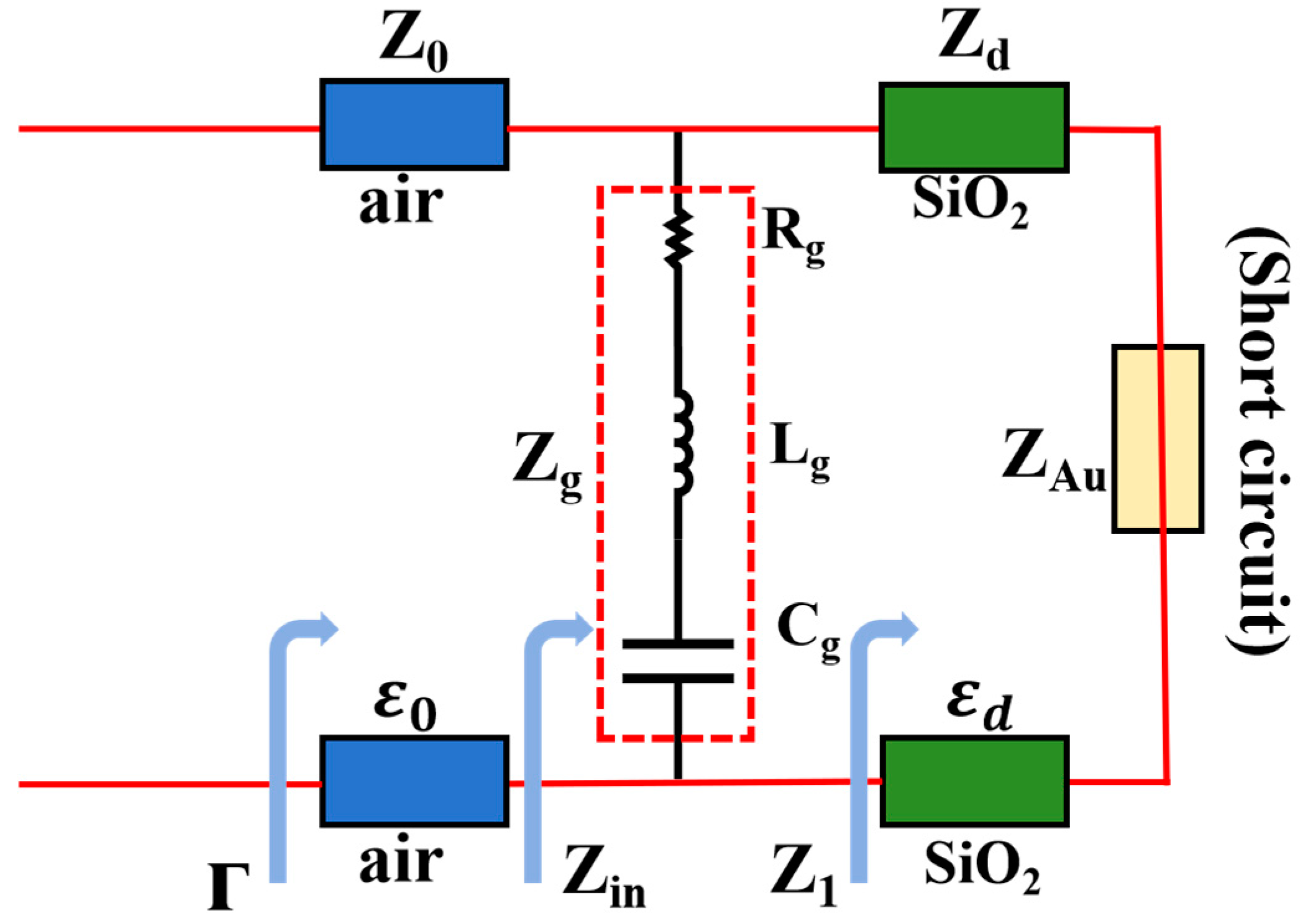
2. Materials and Structure
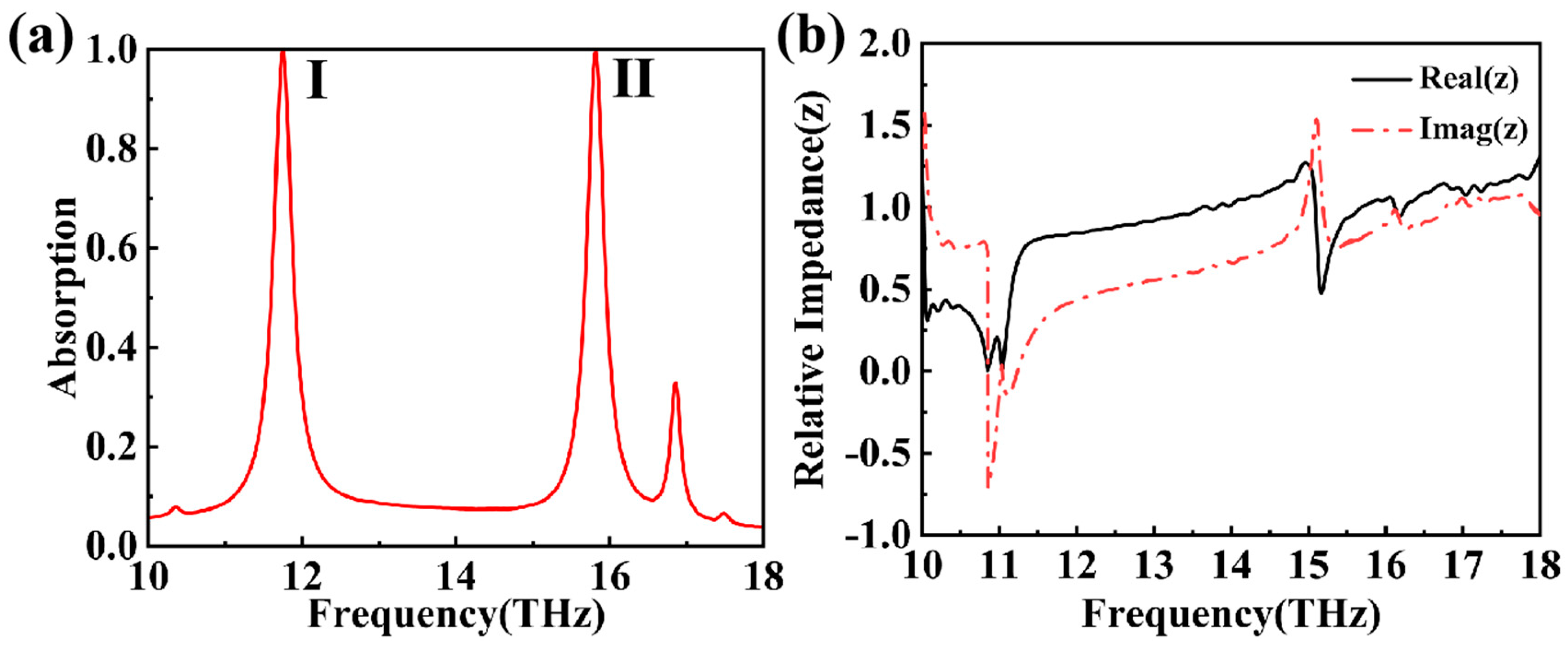
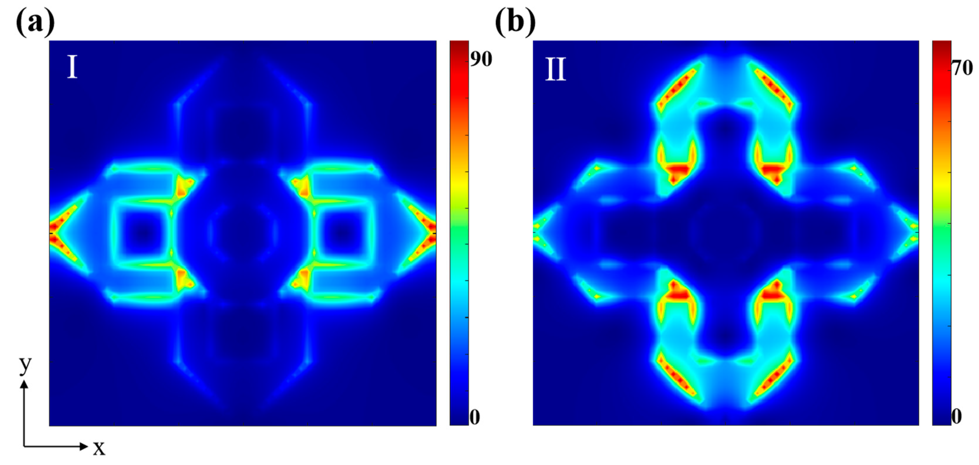
3. Outcomes and Analysis
4. Conclusions
Author Contributions
Funding
Institutional Review Board Statement
Informed Consent Statement
Data Availability Statement
Conflicts of Interest
References
- Berhe, A.M.; As’ham, K.; Al-Ani, I.; Hattori, H.T.; Miroshnichenko, A.E. Strong coupling and catenary field enhancement in the hybrid plasmonic metamaterial cavity and TMDC monolayers. Opto-Electron. Adv. 2024, 7, 230181. [Google Scholar] [CrossRef]
- Wang, Z.; Pan, W.; He, Y.; Zhu, Z.; Jin, X.; Liu, M.; Ma, S.; He, Q.; Sun, S.; Zhou, L.; et al. Efficient generation of vectorial terahertz beams using surface-wave excited metasurfaces. Opto-Electron. Sci. 2025, 4, 240024. [Google Scholar] [CrossRef]
- Liu, M.L.; Li, B.X.; Zeng, L.L.; Wei, Y.; Wen, R.Q.; Zhang, X.J.; Deng, C.S. Dynamic tunable narrow-band perfect absorber for fiber -optic communication band based on liquid crystal. J. Phys. D Appl. Phys. 2023, 56, 505102. [Google Scholar] [CrossRef]
- Jo, Y.; Park, H.; Yoon, H.; Kim, I. Advanced biological imaging techniques based on metasurfaces. Opto-Electron. Adv. 2024, 7, 240122. [Google Scholar] [CrossRef]
- Wang, Q.S.; Fang, Y.; Meng, Y.; Hao, H.; Li, X.; Pu, M.; Ma, X.; Luo, X. Vortex-field enhancement through high-threshold geometric metasurface. Opto-Electron. Adv. 2024, 7, 240112. [Google Scholar] [CrossRef]
- Yang, C.; Luo, M.H.; Ju, X.W.; Hu, J.Y. Ultra-narrow dual-band perfect absorber based on double-slotted silicon nanodisk arrays. J. Phys. D Appl. Phys. 2024, 57, 345104. [Google Scholar] [CrossRef]
- Hu, J.Y.; Bai, W.D.; Tan, C.X.; Li, Y.M.; Lin, Q.; Wang, L.L. Highly electric field enhancement induced by anapole modes coupling in the hybrid dielectric-metal nanoantenna. Opt. Commun. 2022, 511, 127987. [Google Scholar] [CrossRef]
- Zhang, B.W.; Luo, Y.N. Dynamic optical tuning and sensing in L-shaped dirac semimetal-based terahertz metasurfaces. Phys. Lett. A 2025, 541, 130419. [Google Scholar] [CrossRef]
- Yu, Z.; Li, M.; Xing, Z.; Gao, H.; Liu, Z.; Pu, S.; Mao, H.; Cai, H.; Ma, Q.; Ren, W.; et al. Genetic algorithm assisted meta-atom design for high-performance metasurface optics. Opto-Electron. Sci. 2024, 3, 240016. [Google Scholar] [CrossRef]
- Wang, H.Y.; Ma, R.; Liu, G.D.; Wang, L.L.; Lin, Q. Optical force conversion and conveyor belt effect with coupled graphene plasmon waveguide modes. Opt. Express 2023, 31, 32422. [Google Scholar] [CrossRef]
- Chen, Z.Y.; Cheng, S.B.; Zhang, H.F.; Yi, Z.; Tang, B.; Chen, J.; Zhang, J.G.; Tang, C.J. Ultra wideband absorption absorber based on Dirac semimetallic and graphene metamaterials. Phys. Lett. A 2024, 517, 129675. [Google Scholar] [CrossRef]
- Li, B.X.; Liu, M.L.; Wen, R.Q.; Wei, Y.; Zeng, L.L.; Deng, C.S. Dynamic control of Fano-like interference in the graphene periodic structure. J. Phys. D Appl. Phys. 2023, 56, 115104. [Google Scholar] [CrossRef]
- Li, W.; Yi, Y.; Yang, H.; Cheng, S.; Yang, W.X.; Zhang, H.; Yi, Z.; Yi, Y.; Li, H. Active Tunable Terahertz Band-width Absorber Based on single layer Graphene. Commun. Theor. Phys. 2023, 75, 045503. [Google Scholar] [CrossRef]
- Tang, C.J.; Nie, Q.M.; Cai, P.G.; Liu, F.X.; Gu, P.; Yan, Z.D.; Huang, Z.; Zhu, M.W. Ultra-broadband near-infrared absorption enhancement of monolayer graphene by multiple-resonator approach. Diam. Relat. Mater. 2024, 141, 110607. [Google Scholar] [CrossRef]
- Li, Z.T.; Li, X.; Liu, G.D.; Wang, L.L.; Lin, Q. Analytical investigation of unidirectional reflectionless phenomenon near the exceptional points in graphene plasmonic system. Opt. Express 2023, 31, 30458. [Google Scholar] [CrossRef]
- Landy, N.I.; Sajuyigbe, S.; Mock, J.J.; Smith, D.R.; Padilla, W.J. Perfect Metamaterial Absorber. Phys. Rev. Lett. 2008, 100, 207402. [Google Scholar] [CrossRef] [PubMed]
- Chen, S.; Wu, X.H.; Fu, C.J. Active tuning of anisotropic phonon polaritons in natural van der Waals crystals with negative permittivity substrates and its application in energy transport. Opto-Electron. Sci. 2024, 3, 240002. [Google Scholar] [CrossRef]
- Li, Y.M.; Tan, C.X.; Hu, J.Y.; Bai, W.D.; Zhang, R.L.; Lin, Q.; Zhang, Y.; Wang, L.L. Ultra-narrow band perfect absorbance induced by magnetic lattice resonances in dielectric dimer metamaterials. Results Phys. 2022, 39, 105730. [Google Scholar] [CrossRef]
- Sabaruddin, N.R.; Tan, Y.M.; Chen, S.; Chao, C.C.; Lim, C.M.; Thotagamuge, R.; Kooh, M.R.R.; Chau, Y.C. Designing a broadband terahertz metamaterial absorber through Bi-Layer hybridization of metal and graphene. Plasmonics 2024, 19, 3259–3272. [Google Scholar] [CrossRef]
- Li, Z.T.; Cheng, S.B.; Zhang, H.F.; Yang, W.X.; Yi, Z.; Yi, Y.G.; Wang, J.Q.; Ahmad, S.; Raza, R. Ultrathin broadband terahertz metamaterial based on single-layer nested patterned graphene. Phys. Lett. A 2025, 534, 130262. [Google Scholar] [CrossRef]
- Chen, M.; Sun, W.; Cai, J.; Chang, L.; Xiao, X. Frequency-tunable terahertz absorbers based on graphene metasurface. Opt. Commun. 2016, 382, 144–150. [Google Scholar] [CrossRef]
- Yan, D.; Li, J. Tunable all-graphene-dielectric single-band terahertz wave absorber. J. Phys. D Appl. Phys. 2019, 52, 275102. [Google Scholar] [CrossRef]
- Zhu, X.; Wang, B. Graphene-Based Angle-Insensitive and tunable Single-Band and Dual-Band metamaterial terahertz absorber. Phys. Status Solidi (B) 2021, 259, 2100573. [Google Scholar] [CrossRef]
- Hamouleh-Alipour, A.; Mir, A.; Farmani, A. Analytical modeling and design of a graphene metasurface sensor for Thermo-Optical detection of terahertz plasmons. IEEE Sens. J. 2020, 21, 4525–4532. [Google Scholar] [CrossRef]
- Du, X.; Yan, F.; Wang, W.; Zhang, L.; Bai, Z.; Zhou, H.; Hou, Y. Thermally-stable graphene metamaterial absorber with excellent tunability for high-performance refractive index sensing in the terahertz band. Opt. Laser Technol. 2021, 144, 107409. [Google Scholar] [CrossRef]
- Li, B.; Chen, Y.; Wu, Q.; Li, Y.; Wang, J.; Li, F.; Li, N. An ultrathin and dual-band bidirectional metasurface absorber based on ring-disk resonators. Appl. Phys. A 2024, 130, 125. [Google Scholar] [CrossRef]
- Chao, C.C.; Chen, S.; Thotagamuge, R.; Kooh, M.R.R.; Chau, Y.C. Enhancement of Third-Harmonic generation through plasmonic gap and cavity resonance modes in bilayer Graphene/Dielectric/Graphene metasurfaces. Plasmonics 2025, 1–13. [Google Scholar] [CrossRef]
- Mohammadi, G.; Orouji, A.A.; Danaie, M. A tunable narrow single-mode bandpass filter using graphene nanoribbons for THz applications. Sci. Rep. 2024, 14, 21217. [Google Scholar] [CrossRef]
- Yan, D.Y.; Tang, C.J.; Yi, Z.; Wang, J.Q.; Li, B.X. A fully symmetric solar absorber for thermophotovoltaic power generation. Phys. Lett. A 2025, 542, 130461. [Google Scholar] [CrossRef]
- Ling, Z.X.; Zeng, Y.; Liu, G.D.; Wang, L.L.; Lin, Q. Unified model for plasmon-induced transparency with direct and indirect coupling in borophene-integrated metamaterials. Opt. Express 2022, 30, 21966. [Google Scholar] [CrossRef]
- Rao, X.J.; Zhu, H.R.; Wang, X.X.; Chen, Y.Z.; Qi, Y.P.; Yang, H. High-sensitivity plasmonic refractive index sensor based on embedded gratings with triple self-reference characteristics. J. Opt. Soc. Am. B 2025, 42, 431–437. [Google Scholar] [CrossRef]
- Wang, J.Q.; Sun, J.Y.; Sun, S.; Zhang, H.; Wang, Q.Q.; Yang, J.Y.; Mei, Y.W. Numerical simulation of electromagnetically induced transparency in composite metamaterial. Phys. Scr. 2025, 100, 025512. [Google Scholar] [CrossRef]
- Tan, Z.Q.; Lin, Q.; Du, W.J.; Wang, L.L.; Liu, G.D. Simultaneously enhance electric and magnetic Purcell factor by strong coupling between toroidal dipole quasi-BIC and electric dipole. J. Appl. Phys. 2025, 137, 033103. [Google Scholar] [CrossRef]
- Ai, Z.; Liu, H.F.; Cheng, S.B.; Zhang, H.F.; Yi, Z.; Zeng, Q.D.; Wu, P.H.; Zhang, J.G.; Tang, C.J.; Hao, Z.Q. Four peak and high angle tilted insensitive surface plasmon resonance graphene absorber based on circular etching square window. J. Phys. D Appl. Phys. 2025, 58, 185305. [Google Scholar] [CrossRef]
- Ma, R.; Zhang, L.G.; Zeng, Y.; Liu, G.D.; Wang, L.L.; Lin, Q. Extreme enhancement of optical force via the acoustic graphene plasmon mode. Opt. Express 2023, 31, 482723. [Google Scholar] [CrossRef]
- Wei, T.; Hauke, F.; Hirsch, A. Evolution of graphene patterning: From dimension regulation to Molecular Engineering. Adv. Mater. 2021, 33, 2104060. [Google Scholar] [CrossRef]
- Huang, Z.; Liu, G.D.; Wang, L. Active modulation of quasi-bound state in the continuum based on bulk Dirac semimetals metamaterial. Appl. Phys. Express 2022, 15, 032006. [Google Scholar] [CrossRef]
- Li, Z.; Song, Q.J.; Jia, L.B.; Yi, Z.; Cheng, S.B.; Wang, J.Q.; Li, B.X. Actively tunable multi-frequency narrowband terahertz absorber using graphene metamaterials. Opt. Commun. 2025, 583, 131768. [Google Scholar] [CrossRef]
- Zeng, Y.; Ling, Z.X.; Liu, G.D.; Wang, L.L.; Lin, Q. Tunable plasmonically induced transparency with giant group delay in gain-assisted graphene metamaterials. Opt. Express 2022, 30, 455954. [Google Scholar] [CrossRef]
- Yang, Q.; Yu, M.; Chen, Z.; Ai, S.; Kentsch, U.; Zhou, S.; Jia, Y.; Chen, F.; Liu, H. A novel approach towards robust construction of physical colors on lithium niobate crystal. Opto-Electron. Adv. 2025, 8, 240193. [Google Scholar] [CrossRef]
- Zhang, S.W.; Yang, H.; Tang, C.J.; Yi, Z.; Zhang, J.G.; Wang, J.Q.; Li, B.X. Multiple tunable six-peak graphene absorber for high-performance refractive index sensing. Phys. B Condens. Matter 2025, 708, 417225. [Google Scholar] [CrossRef]
- Zeng, T.Y.; Liu, G.D.; Wang, L.L.; Lin, Q. Light-matter interactions enhanced by quasi-bound states in the continuum in a graphene-dielectric metasurface. Opt. Express 2021, 29, 40177–40186. [Google Scholar] [CrossRef]
- Jia, Z.; Huang, L.; Su, J.; Tang, B. Tunable Electromagnetically Induced Transparency-Like in Graphene metasurfaces and its Application as a Refractive Index Sensor. J. Light. Technol. 2021, 39, 1544–1549. [Google Scholar] [CrossRef]
- Zhang, Y.X.; Lin, Q.; Yan, X.Q.; Wang, L.L.; Liu, G.D. Flat-band Friedrich-Wintgen bound states in the continuum based on borophene metamaterials. Opt. Express 2024, 32, 10669–10678. [Google Scholar] [CrossRef]
- Li, W.X.; Cheng, S.B.; Yi, Z.; Zhang, H.F.; Song, Q.J.; Hao, Z.Q.; Sun, T.Y.; Wu, P.H.; Zeng, Q.D.; Raza, R. Advanced optical reinforcement materials based on three-dimensional four-way weaving structure and metasurface technology. Appl. Phys. Lett. 2025, 126, 033503. [Google Scholar] [CrossRef]
- Lv, J.; Ren, Y.; Wang, D.; Wang, J.; Lu, X.; Yu, Y.; Li, W.; Liu, Q.; Xu, X.; Liu, W.; et al. Optical switching with high-Q Fano resonance of all-dielectric metasurface governed by bound states in the continuum. Opt. Express 2024, 32, 28334–28347. [Google Scholar] [CrossRef]
- Wang, Y.J.; Liu, Z.M.; Zhou, F.Q.; Yi, Z.; Wang, J.Q. Perfect absorption properties of a near-infrared super-surface perfect absorber based on a multilayer subwavelength array structure. Phys. Lett. A 2025, 540, 130395. [Google Scholar] [CrossRef]
- Luo, M.H.; Hu, J.Y.; Li, Y.M.; Bai, W.D.; Zhang, R.L.; Lin, Q.; Wang, L.L. Anapole-assisted ultra-narrow-band lattice resonance in slotted silicon nanodisk arrays. J. Phys. D Appl. Phys. 2023, 56, 375102. [Google Scholar] [CrossRef]
- Yang, C.; Guo, C.M.; Xu, J.; Zhang, H.-F. Device Design for Multitask Graphene Electromagnetic Detection Based on Second Harmonic Generation. IEEE Trans. Microw. Theory Tech. 2024, 72, 4174–4182. [Google Scholar] [CrossRef]
- Li, W.; Cheng, S.; Zhang, H.; Yi, Z.; Tang, B.; Ma, C.; Wu, P.; Zeng, Q.; Raza, R. Multi-functional metasurface: Ultra-wideband/multi-band absorption switching by adjusting guided mode resonance and local surface plasmon resonance effects. Commun. Theor. Phys. 2024, 76, 065701. [Google Scholar] [CrossRef]
- Wang, J.Q.; Yang, J.Y.; Mei, Y.W. Non-radiating anapole state in dielectric nanostructures and metamaterials. J. Phys. D Appl. Phys. 2025, 58, 203001. [Google Scholar] [CrossRef]
- Abdulkarim, Y.I. Switchable and Tunable Terahertz Metamaterial Absorber with Ultra-Broadband and Multi-Band Response for Cancer Detection. Sensors 2025, 25, 1463. [Google Scholar] [CrossRef] [PubMed]
- Long, T.; Zhang, L.; Wang, L.L.; Lin, Q. Tunable narrow transparency windows induced by the coupled quasi-guided modes in borophene plasmonic nanostructure. J. Phys. D Appl. Phys. 2022, 55, 315101. [Google Scholar] [CrossRef]
- Wang, J.; Zhu, H.; Ni, B.; Zhou, M.; Feng, C.; Ni, H.; Chang, J. Simple Design of Polarization-Selective Tunable Triple Terahertz Absorber Based on Graphene Rectangular Ring Resonator. Photonics 2024, 11, 1160. [Google Scholar] [CrossRef]
- Li, X.; Li, Z.T.; Wang, L.L.; Lin, Q. Unidirectional reflectionless propagation in borophene plasmonic metamaterials. J. Phys. D Appl. Phys. 2023, 57, 015103. [Google Scholar] [CrossRef]
- Yang, J.P.; Tang, A.; Lian, B.W.; Xiong, Z.J.; Ma, Z.B.; Gu, N.T. Optimal multi-spectrum polarization detection with full-Stokes in a single channel by using standard retarders. Measurement 2025, 242, 116052. [Google Scholar] [CrossRef]
- Xiang, T.; Sun, Z.; Wang, L.L.; Lin, Q.; Liu, G.D. Polarization independent perfect absorption of borophene metamaterials operating in the communication band. Phys. Scr. 2024, 99, 085519. [Google Scholar] [CrossRef]
- Xiong, H.; Yang, Q.; Huang, Y.Z.; Deng, J.H. High-Efficiency Microwave Wireless Power Transmission via Reflective Phase Gradient Metasurfaces and Surface Wave Aggregation. ACS Appl. Mater. Interfaces 2024, 16, 60189–60196. [Google Scholar] [CrossRef]
- Hu, Z.; Zhao, Y.; Zou, W.; Lu, Q.; Liao, J.; Li, F.; Shang, M.; Lin, L.; Liu, Z. Doping of Graphene Films: Open the way to Applications in Electronics and Optoelectronics. Adv. Funct. Mater. 2022, 32, 2203179. [Google Scholar] [CrossRef]
- Peng, L.; Li, X.; Liu, X.; Jiang, X.; Li, S. Metal and graphene hybrid metasurface designed ultra-wideband terahertz absorbers with polarization and incident angle insensitivity. Nanoscale Adv. 2019, 1, 1452–1459. [Google Scholar] [CrossRef]
- Xie, T.; Chen, D.; Yang, H.; Xu, Y.; Zhang, Z.; Yang, J. Tunable Broadband Terahertz Waveband Absorbers Based on Fractal Technology of Graphene Metamaterial. Nanomaterials 2021, 11, 269. [Google Scholar] [CrossRef] [PubMed]
- Ma, R.; Zhang, L.; Liu, G.; Wang, L.; Lin, Q. The total optical force exerted on black phosphorus coated dielectric cylinder pairs enhanced by localized surface plasmon. J. Appl. Phys. 2021, 130, 113103. [Google Scholar] [CrossRef]
- Zeng, L.L.; Li, B.X.; Wen, R.Q.; Zhang, X.J. Plasmonic Sensor Based on Multi Fano Resonance in Inverse T Shape Structure for Detection of CO2 Concentration. IEEE Photonics J. 2023, 15, 2201805. [Google Scholar] [CrossRef]
- Wang, X.Y.; Lin, Q.; Wang, L.L.; Liu, G.D. Dynamic control of polarization conversion based on borophene nanostructures in optical communication bands. Phys. Scr. 2024, 99, 085531. [Google Scholar] [CrossRef]
- Cheng, S.B.; Li, W.X.; Zhang, H.F.; Akhtar, M.N.; Yi, Z.; Zeng, Q.D.; Ma, C.; Sun, T.Y.; Wu, P.H.; Ahmad, S. High sensitivity five band tunable metamaterial absorption device based on block like Dirac semimetals. Opt. Commun. 2024, 569, 130816. [Google Scholar] [CrossRef]
- Hu, J.Y.; Tan, C.X.; Bai, W.D.; Li, Y.M.; Lin, Q.; Wang, L.L. Dielectric nanocavity-coupled surface lattice resonances for high-efficiency plasmonic sensing. J. Phys. D Appl. Phys. 2022, 55, 075105. [Google Scholar] [CrossRef]
- Li, B.X.; Zeng, L.L.; Wen, R.Q.; Zhang, X.J. Dynamic Regulation of Multiple Fano Resonances Based on Liquid Crystal. IEEE Photonics J. 2023, 15, 2200506. [Google Scholar] [CrossRef]
- Zeng, Z.L.; Liu, H.F.; Zhang, H.F.; Cheng, S.B.; Yi, Y.G.; Yi, Z.; Wang, J.Q.; Zhang, J.G. Tunable ultra-sensitive four-band terahertz sensors based on Dirac semimetals. Photonics Nanostruct.-Fundam. Appl. 2025, 63, 101347. [Google Scholar] [CrossRef]
- Gu, X.; Liu, X.; Yan, X.F.; Du, W.J.; Lin, Q.; Wang, L.L.; Liu, G.D. Polaritonic coherent perfect absorption based on self-hybridization of a quasi-bound state in the continuum and exciton. Opt. Express 2023, 31, 4691–4700. [Google Scholar] [CrossRef]
- Liu, J.; Dai, H.; Ju, J.; Cheng, K. Perfect absorber with high sensitivity based on hexagonal star graphene surface. Surf. Interfaces 2023, 39, 102985. [Google Scholar] [CrossRef]
- Khodadadi, B.; Rezaei, P.; Hadipour, S. Dual-band Polarization-independent Maze-shaped Absorber based on Graphene for Terahertz Biomedical Sensing. Opt. Express 2024, 33, 3869–3880. [Google Scholar] [CrossRef]
- Veeraselvam, A.; Mohammed, G.N.A.; Savarimuthu, K. A novel Ultra-Miniaturized Highly Sensitive Refractive Index-Based Terahertz biosensor. J. Light. Technol. 2021, 39, 7281–7287. [Google Scholar] [CrossRef]
- Zhu, A.; Bu, P.; Cheng, L.; Hu, C.; Mahapatra, R. High-Q Multiband Narrowband Absorbers Based on Two-Dimensional Graphene Metamaterials. Photonics 2024, 11, 469. [Google Scholar] [CrossRef]
- Almawgani, A.H.M.; Surve, J.; Parmar, T.; Armghan, A.; Aliqab, K.; Ali, G.A.; Patel, S.K. A Graphene-Metasurface-Inspired Optical Sensor for the Heavy Metals Detection for Efficient and Rapid Water Treatment. Photonics 2023, 10, 56. [Google Scholar] [CrossRef]
- Khodadadi, B.; Babaeinik, M.; Ghods, V.; Rezaei, P. Triple-band metamaterial perfect absorber for refractive index sensing in THz frequency. Opt. Quant. Electron. 2023, 55, 431. [Google Scholar] [CrossRef]


| Source | Materials | Peak Count | Mean Absorption Rate | Sensitivity [THz/RIU] | FOM | Q-Factor |
|---|---|---|---|---|---|---|
| [25] | Graphene | 2 | 96.05% | 1.84 | ~ | ~ |
| [70] | Graphene | 2 | 99.5% | 0.984 | 3.57 | 14.54 |
| [71] | Graphene | 2 | 98.41% | 1.15 | 1.55 | 8.92 |
| [72] | metal layer | 1 | 99% | 2.1 | 7.03 | ~ |
| [73] | Graphene | 3 | 97.93% | 0.382 | 3.24 | 58.64 |
| [74] | Graphene | 1 | 76.17% | 0.114 | 3.15 | 11.2 |
| [75] | Graphene | 3 | 99.53% | 1.86 | 2.14 | ~ |
| This work | Graphene | 2 | 99.8% | 3.205 | 11.301 | 48.61 |
Disclaimer/Publisher’s Note: The statements, opinions and data contained in all publications are solely those of the individual author(s) and contributor(s) and not of MDPI and/or the editor(s). MDPI and/or the editor(s) disclaim responsibility for any injury to people or property resulting from any ideas, methods, instructions or products referred to in the content. |
© 2025 by the authors. Licensee MDPI, Basel, Switzerland. This article is an open access article distributed under the terms and conditions of the Creative Commons Attribution (CC BY) license (https://creativecommons.org/licenses/by/4.0/).
Share and Cite
Zhang, S.; Chen, K.; Sun, T.; Song, Q.; Yi, Z.; Yi, Y. Highly Sensitive and Tunable Graphene Metamaterial Perfect Absorber in the Near-Terahertz Band. Coatings 2025, 15, 512. https://doi.org/10.3390/coatings15050512
Zhang S, Chen K, Sun T, Song Q, Yi Z, Yi Y. Highly Sensitive and Tunable Graphene Metamaterial Perfect Absorber in the Near-Terahertz Band. Coatings. 2025; 15(5):512. https://doi.org/10.3390/coatings15050512
Chicago/Turabian StyleZhang, Siwen, Kele Chen, Tangyou Sun, Qianju Song, Zao Yi, and Yougen Yi. 2025. "Highly Sensitive and Tunable Graphene Metamaterial Perfect Absorber in the Near-Terahertz Band" Coatings 15, no. 5: 512. https://doi.org/10.3390/coatings15050512
APA StyleZhang, S., Chen, K., Sun, T., Song, Q., Yi, Z., & Yi, Y. (2025). Highly Sensitive and Tunable Graphene Metamaterial Perfect Absorber in the Near-Terahertz Band. Coatings, 15(5), 512. https://doi.org/10.3390/coatings15050512